
Vivado Design Suite
Properties Reference
Guide
UG912 (v2022.1) June 8, 2022
Xilinx is creating an environment where employees, customers,
and partners feel welcome and included. To that end, we’re
removing non-inclusive language from our products and related
collateral. We’ve launched an internal initiative to remove
language that could exclude people or reinforce historical biases,
including terms embedded in our software and IPs. You may still
find examples of non-inclusive language in our older products as
we work to make these changes and align with evolving industry
standards. Follow this link for more information.

Vivado Properties Reference 2
UG912 (v2022.1) June 8, 2022 www.xilinx.com
Table of Contents
Chapter 1: Vivado Design Suite First Class Objects
Navigating Content by Design Process . . . . . . . . . . . . . . . . . . . . . . . . . . . . . . . . . . . . . . . . . . . . . . . . . 8
Introduction . . . . . . . . . . . . . . . . . . . . . . . . . . . . . . . . . . . . . . . . . . . . . . . . . . . . . . . . . . . . . . . . . . . . . . 8
Copying Examples from this Document . . . . . . . . . . . . . . . . . . . . . . . . . . . . . . . . . . . . . . . . . . . . . . . . 9
Netlist and Device Objects . . . . . . . . . . . . . . . . . . . . . . . . . . . . . . . . . . . . . . . . . . . . . . . . . . . . . . . . . 10
Block Design Objects . . . . . . . . . . . . . . . . . . . . . . . . . . . . . . . . . . . . . . . . . . . . . . . . . . . . . . . . . . . . . . 13
Hardware Manager Objects . . . . . . . . . . . . . . . . . . . . . . . . . . . . . . . . . . . . . . . . . . . . . . . . . . . . . . . . 15
Chapter 2: Alphabetical List of First Class Objects
BD_ADDR_SEG . . . . . . . . . . . . . . . . . . . . . . . . . . . . . . . . . . . . . . . . . . . . . . . . . . . . . . . . . . . . . . . . . . . 17
BD_ADDR_SPACE . . . . . . . . . . . . . . . . . . . . . . . . . . . . . . . . . . . . . . . . . . . . . . . . . . . . . . . . . . . . . . . . . 20
BD_CELL . . . . . . . . . . . . . . . . . . . . . . . . . . . . . . . . . . . . . . . . . . . . . . . . . . . . . . . . . . . . . . . . . . . . . . . . 22
BD_INTF_NET . . . . . . . . . . . . . . . . . . . . . . . . . . . . . . . . . . . . . . . . . . . . . . . . . . . . . . . . . . . . . . . . . . . . 24
BD_INTF_PIN . . . . . . . . . . . . . . . . . . . . . . . . . . . . . . . . . . . . . . . . . . . . . . . . . . . . . . . . . . . . . . . . . . . . 26
BD_INTF_PORT. . . . . . . . . . . . . . . . . . . . . . . . . . . . . . . . . . . . . . . . . . . . . . . . . . . . . . . . . . . . . . . . . . . 29
BD_NET . . . . . . . . . . . . . . . . . . . . . . . . . . . . . . . . . . . . . . . . . . . . . . . . . . . . . . . . . . . . . . . . . . . . . . . . . 31
BD_PIN . . . . . . . . . . . . . . . . . . . . . . . . . . . . . . . . . . . . . . . . . . . . . . . . . . . . . . . . . . . . . . . . . . . . . . . . . 33
BD_PORT. . . . . . . . . . . . . . . . . . . . . . . . . . . . . . . . . . . . . . . . . . . . . . . . . . . . . . . . . . . . . . . . . . . . . . . . 35
BEL. . . . . . . . . . . . . . . . . . . . . . . . . . . . . . . . . . . . . . . . . . . . . . . . . . . . . . . . . . . . . . . . . . . . . . . . . . . . . 37
BEL_PIN. . . . . . . . . . . . . . . . . . . . . . . . . . . . . . . . . . . . . . . . . . . . . . . . . . . . . . . . . . . . . . . . . . . . . . . . . 41
CELL . . . . . . . . . . . . . . . . . . . . . . . . . . . . . . . . . . . . . . . . . . . . . . . . . . . . . . . . . . . . . . . . . . . . . . . . . . . . 43
CLOCK . . . . . . . . . . . . . . . . . . . . . . . . . . . . . . . . . . . . . . . . . . . . . . . . . . . . . . . . . . . . . . . . . . . . . . . . . . 47
CLOCK_REGION . . . . . . . . . . . . . . . . . . . . . . . . . . . . . . . . . . . . . . . . . . . . . . . . . . . . . . . . . . . . . . . . . . 50
DIAGRAM . . . . . . . . . . . . . . . . . . . . . . . . . . . . . . . . . . . . . . . . . . . . . . . . . . . . . . . . . . . . . . . . . . . . . . . 53
HW_AXI. . . . . . . . . . . . . . . . . . . . . . . . . . . . . . . . . . . . . . . . . . . . . . . . . . . . . . . . . . . . . . . . . . . . . . . . . 54
HW_BITSTREAM. . . . . . . . . . . . . . . . . . . . . . . . . . . . . . . . . . . . . . . . . . . . . . . . . . . . . . . . . . . . . . . . . . 56
HW_CFGMEM. . . . . . . . . . . . . . . . . . . . . . . . . . . . . . . . . . . . . . . . . . . . . . . . . . . . . . . . . . . . . . . . . . . . 58
HW_DEVICE . . . . . . . . . . . . . . . . . . . . . . . . . . . . . . . . . . . . . . . . . . . . . . . . . . . . . . . . . . . . . . . . . . . . . 60
HW_ILA . . . . . . . . . . . . . . . . . . . . . . . . . . . . . . . . . . . . . . . . . . . . . . . . . . . . . . . . . . . . . . . . . . . . . . . . . 63
HW_ILA_DATA . . . . . . . . . . . . . . . . . . . . . . . . . . . . . . . . . . . . . . . . . . . . . . . . . . . . . . . . . . . . . . . . . . . 66
HW_PROBE. . . . . . . . . . . . . . . . . . . . . . . . . . . . . . . . . . . . . . . . . . . . . . . . . . . . . . . . . . . . . . . . . . . . . . 67
HW_SERVER . . . . . . . . . . . . . . . . . . . . . . . . . . . . . . . . . . . . . . . . . . . . . . . . . . . . . . . . . . . . . . . . . . . . . 70
HW_SIO_GT . . . . . . . . . . . . . . . . . . . . . . . . . . . . . . . . . . . . . . . . . . . . . . . . . . . . . . . . . . . . . . . . . . . . . 71

Vivado Properties Reference 3
UG912 (v2022.1) June 8, 2022 www.xilinx.com
HW_SIO_GTGROUP . . . . . . . . . . . . . . . . . . . . . . . . . . . . . . . . . . . . . . . . . . . . . . . . . . . . . . . . . . . . . . . 81
HW_SIO_IBERT . . . . . . . . . . . . . . . . . . . . . . . . . . . . . . . . . . . . . . . . . . . . . . . . . . . . . . . . . . . . . . . . . . . 82
HW_SIO_PLL . . . . . . . . . . . . . . . . . . . . . . . . . . . . . . . . . . . . . . . . . . . . . . . . . . . . . . . . . . . . . . . . . . . . . 84
HW_SIO_RX . . . . . . . . . . . . . . . . . . . . . . . . . . . . . . . . . . . . . . . . . . . . . . . . . . . . . . . . . . . . . . . . . . . . . 86
HW_SIO_TX . . . . . . . . . . . . . . . . . . . . . . . . . . . . . . . . . . . . . . . . . . . . . . . . . . . . . . . . . . . . . . . . . . . . . 92
HW_SYSMON . . . . . . . . . . . . . . . . . . . . . . . . . . . . . . . . . . . . . . . . . . . . . . . . . . . . . . . . . . . . . . . . . . . . 96
HW_TARGET . . . . . . . . . . . . . . . . . . . . . . . . . . . . . . . . . . . . . . . . . . . . . . . . . . . . . . . . . . . . . . . . . . . . 100
HW_VIO . . . . . . . . . . . . . . . . . . . . . . . . . . . . . . . . . . . . . . . . . . . . . . . . . . . . . . . . . . . . . . . . . . . . . . . 102
IO_BANK . . . . . . . . . . . . . . . . . . . . . . . . . . . . . . . . . . . . . . . . . . . . . . . . . . . . . . . . . . . . . . . . . . . . . . . 104
IO_STANDARD . . . . . . . . . . . . . . . . . . . . . . . . . . . . . . . . . . . . . . . . . . . . . . . . . . . . . . . . . . . . . . . . . . 106
NET . . . . . . . . . . . . . . . . . . . . . . . . . . . . . . . . . . . . . . . . . . . . . . . . . . . . . . . . . . . . . . . . . . . . . . . . . . . 108
NODE. . . . . . . . . . . . . . . . . . . . . . . . . . . . . . . . . . . . . . . . . . . . . . . . . . . . . . . . . . . . . . . . . . . . . . . . . . 112
PACKAGE_PIN. . . . . . . . . . . . . . . . . . . . . . . . . . . . . . . . . . . . . . . . . . . . . . . . . . . . . . . . . . . . . . . . . . . 114
PIN . . . . . . . . . . . . . . . . . . . . . . . . . . . . . . . . . . . . . . . . . . . . . . . . . . . . . . . . . . . . . . . . . . . . . . . . . . . 116
PIP or SITE_PIP . . . . . . . . . . . . . . . . . . . . . . . . . . . . . . . . . . . . . . . . . . . . . . . . . . . . . . . . . . . . . . . . . . 119
PKGPIN_BYTEGROUP. . . . . . . . . . . . . . . . . . . . . . . . . . . . . . . . . . . . . . . . . . . . . . . . . . . . . . . . . . . . . 122
PKGPIN_NIBBLE . . . . . . . . . . . . . . . . . . . . . . . . . . . . . . . . . . . . . . . . . . . . . . . . . . . . . . . . . . . . . . . . . 124
PORT . . . . . . . . . . . . . . . . . . . . . . . . . . . . . . . . . . . . . . . . . . . . . . . . . . . . . . . . . . . . . . . . . . . . . . . . . . 126
SITE . . . . . . . . . . . . . . . . . . . . . . . . . . . . . . . . . . . . . . . . . . . . . . . . . . . . . . . . . . . . . . . . . . . . . . . . . . . 129
SLR. . . . . . . . . . . . . . . . . . . . . . . . . . . . . . . . . . . . . . . . . . . . . . . . . . . . . . . . . . . . . . . . . . . . . . . . . . . . 133
TILE . . . . . . . . . . . . . . . . . . . . . . . . . . . . . . . . . . . . . . . . . . . . . . . . . . . . . . . . . . . . . . . . . . . . . . . . . . . 135
TIMING_PATH . . . . . . . . . . . . . . . . . . . . . . . . . . . . . . . . . . . . . . . . . . . . . . . . . . . . . . . . . . . . . . . . . . 139
WIRE . . . . . . . . . . . . . . . . . . . . . . . . . . . . . . . . . . . . . . . . . . . . . . . . . . . . . . . . . . . . . . . . . . . . . . . . . . 142
Chapter 3: Key Property Descriptions
Properties Information . . . . . . . . . . . . . . . . . . . . . . . . . . . . . . . . . . . . . . . . . . . . . . . . . . . . . . . . . . . 144
ASYNC_REG . . . . . . . . . . . . . . . . . . . . . . . . . . . . . . . . . . . . . . . . . . . . . . . . . . . . . . . . . . . . . . . . . . . . 145
AUTO_INCREMENTAL_CHECKPOINT . . . . . . . . . . . . . . . . . . . . . . . . . . . . . . . . . . . . . . . . . . . . . . . . 149
AUTOPIPELINE_GROUP . . . . . . . . . . . . . . . . . . . . . . . . . . . . . . . . . . . . . . . . . . . . . . . . . . . . . . . . . . . 151
AUTOPIPELINE_MODULE. . . . . . . . . . . . . . . . . . . . . . . . . . . . . . . . . . . . . . . . . . . . . . . . . . . . . . . . . . 153
AUTOPIPELINE_INCLUDE . . . . . . . . . . . . . . . . . . . . . . . . . . . . . . . . . . . . . . . . . . . . . . . . . . . . . . . . . . 154
AUTOPIPELINE_LIMIT . . . . . . . . . . . . . . . . . . . . . . . . . . . . . . . . . . . . . . . . . . . . . . . . . . . . . . . . . . . . 156
BEL. . . . . . . . . . . . . . . . . . . . . . . . . . . . . . . . . . . . . . . . . . . . . . . . . . . . . . . . . . . . . . . . . . . . . . . . . . . . 157
BLACK_BOX. . . . . . . . . . . . . . . . . . . . . . . . . . . . . . . . . . . . . . . . . . . . . . . . . . . . . . . . . . . . . . . . . . . . . 160
BLI . . . . . . . . . . . . . . . . . . . . . . . . . . . . . . . . . . . . . . . . . . . . . . . . . . . . . . . . . . . . . . . . . . . . . . . . . . . . 162
BLOCK_SYNTH . . . . . . . . . . . . . . . . . . . . . . . . . . . . . . . . . . . . . . . . . . . . . . . . . . . . . . . . . . . . . . . . . . 163
BUFFER_TYPE . . . . . . . . . . . . . . . . . . . . . . . . . . . . . . . . . . . . . . . . . . . . . . . . . . . . . . . . . . . . . . . . . . . 165
CARRY_REMAP. . . . . . . . . . . . . . . . . . . . . . . . . . . . . . . . . . . . . . . . . . . . . . . . . . . . . . . . . . . . . . . . . . 166
CASCADE_HEIGHT . . . . . . . . . . . . . . . . . . . . . . . . . . . . . . . . . . . . . . . . . . . . . . . . . . . . . . . . . . . . . . . 168
CELL_BLOAT_FACTOR . . . . . . . . . . . . . . . . . . . . . . . . . . . . . . . . . . . . . . . . . . . . . . . . . . . . . . . . . . . . 169

Vivado Properties Reference 4
UG912 (v2022.1) June 8, 2022 www.xilinx.com
CFGBVS . . . . . . . . . . . . . . . . . . . . . . . . . . . . . . . . . . . . . . . . . . . . . . . . . . . . . . . . . . . . . . . . . . . . . . . . 171
CLOCK_BUFFER_TYPE . . . . . . . . . . . . . . . . . . . . . . . . . . . . . . . . . . . . . . . . . . . . . . . . . . . . . . . . . . . . 173
CLOCK_DEDICATED_ROUTE. . . . . . . . . . . . . . . . . . . . . . . . . . . . . . . . . . . . . . . . . . . . . . . . . . . . . . . . 175
CLOCK_DELAY_GROUP . . . . . . . . . . . . . . . . . . . . . . . . . . . . . . . . . . . . . . . . . . . . . . . . . . . . . . . . . . . 178
CLOCK_LOW_FANOUT . . . . . . . . . . . . . . . . . . . . . . . . . . . . . . . . . . . . . . . . . . . . . . . . . . . . . . . . . . . . 180
CLOCK_REGION . . . . . . . . . . . . . . . . . . . . . . . . . . . . . . . . . . . . . . . . . . . . . . . . . . . . . . . . . . . . . . . . . 183
CLOCK_ROOT . . . . . . . . . . . . . . . . . . . . . . . . . . . . . . . . . . . . . . . . . . . . . . . . . . . . . . . . . . . . . . . . . . . 185
CONFIG_MODE. . . . . . . . . . . . . . . . . . . . . . . . . . . . . . . . . . . . . . . . . . . . . . . . . . . . . . . . . . . . . . . . . . 187
CONFIG_VOLTAGE . . . . . . . . . . . . . . . . . . . . . . . . . . . . . . . . . . . . . . . . . . . . . . . . . . . . . . . . . . . . . . . 189
CONTAIN_ROUTING. . . . . . . . . . . . . . . . . . . . . . . . . . . . . . . . . . . . . . . . . . . . . . . . . . . . . . . . . . . . . . 191
CONTROL_SET_REMAP . . . . . . . . . . . . . . . . . . . . . . . . . . . . . . . . . . . . . . . . . . . . . . . . . . . . . . . . . . . 193
DCI_CASCADE . . . . . . . . . . . . . . . . . . . . . . . . . . . . . . . . . . . . . . . . . . . . . . . . . . . . . . . . . . . . . . . . . . . 195
DELAY_BYPASS. . . . . . . . . . . . . . . . . . . . . . . . . . . . . . . . . . . . . . . . . . . . . . . . . . . . . . . . . . . . . . . . . . 197
DELAY_VALUE_XPHY . . . . . . . . . . . . . . . . . . . . . . . . . . . . . . . . . . . . . . . . . . . . . . . . . . . . . . . . . . . . . 198
DIFF_TERM . . . . . . . . . . . . . . . . . . . . . . . . . . . . . . . . . . . . . . . . . . . . . . . . . . . . . . . . . . . . . . . . . . . . . 200
DIFF_TERM_ADV . . . . . . . . . . . . . . . . . . . . . . . . . . . . . . . . . . . . . . . . . . . . . . . . . . . . . . . . . . . . . . . . 203
DIRECT_ENABLE . . . . . . . . . . . . . . . . . . . . . . . . . . . . . . . . . . . . . . . . . . . . . . . . . . . . . . . . . . . . . . . . . 205
DIRECT_RESET . . . . . . . . . . . . . . . . . . . . . . . . . . . . . . . . . . . . . . . . . . . . . . . . . . . . . . . . . . . . . . . . . . 207
DONT_TOUCH. . . . . . . . . . . . . . . . . . . . . . . . . . . . . . . . . . . . . . . . . . . . . . . . . . . . . . . . . . . . . . . . . . . 209
DQS_BIAS . . . . . . . . . . . . . . . . . . . . . . . . . . . . . . . . . . . . . . . . . . . . . . . . . . . . . . . . . . . . . . . . . . . . . . 213
DRIVE . . . . . . . . . . . . . . . . . . . . . . . . . . . . . . . . . . . . . . . . . . . . . . . . . . . . . . . . . . . . . . . . . . . . . . . . . 216
EDIF_EXTRA_SEARCH_PATHS . . . . . . . . . . . . . . . . . . . . . . . . . . . . . . . . . . . . . . . . . . . . . . . . . . . . . . 218
EQUALIZATION . . . . . . . . . . . . . . . . . . . . . . . . . . . . . . . . . . . . . . . . . . . . . . . . . . . . . . . . . . . . . . . . . . 219
EQUIVALENT_DRIVER_OPT . . . . . . . . . . . . . . . . . . . . . . . . . . . . . . . . . . . . . . . . . . . . . . . . . . . . . . . . 221
EXCLUDE_PLACEMENT. . . . . . . . . . . . . . . . . . . . . . . . . . . . . . . . . . . . . . . . . . . . . . . . . . . . . . . . . . . . 223
EXTRACT_ENABLE . . . . . . . . . . . . . . . . . . . . . . . . . . . . . . . . . . . . . . . . . . . . . . . . . . . . . . . . . . . . . . . 225
EXTRACT_RESET . . . . . . . . . . . . . . . . . . . . . . . . . . . . . . . . . . . . . . . . . . . . . . . . . . . . . . . . . . . . . . . . . 227
FORCE_MAX_FANOUT. . . . . . . . . . . . . . . . . . . . . . . . . . . . . . . . . . . . . . . . . . . . . . . . . . . . . . . . . . . . 229
FSM_ENCODING. . . . . . . . . . . . . . . . . . . . . . . . . . . . . . . . . . . . . . . . . . . . . . . . . . . . . . . . . . . . . . . . . 230
FSM_SAFE_STATE. . . . . . . . . . . . . . . . . . . . . . . . . . . . . . . . . . . . . . . . . . . . . . . . . . . . . . . . . . . . . . . . 232
GATED_CLOCK . . . . . . . . . . . . . . . . . . . . . . . . . . . . . . . . . . . . . . . . . . . . . . . . . . . . . . . . . . . . . . . . . . 234
GENERATE_SYNTH_CHECKPOINT . . . . . . . . . . . . . . . . . . . . . . . . . . . . . . . . . . . . . . . . . . . . . . . . . . . 236
H_SET and HU_SET. . . . . . . . . . . . . . . . . . . . . . . . . . . . . . . . . . . . . . . . . . . . . . . . . . . . . . . . . . . . . . . 238
HIODELAY_GROUP . . . . . . . . . . . . . . . . . . . . . . . . . . . . . . . . . . . . . . . . . . . . . . . . . . . . . . . . . . . . . . . 242
HLUTNM . . . . . . . . . . . . . . . . . . . . . . . . . . . . . . . . . . . . . . . . . . . . . . . . . . . . . . . . . . . . . . . . . . . . . . . 245
IBUF_LOW_PWR . . . . . . . . . . . . . . . . . . . . . . . . . . . . . . . . . . . . . . . . . . . . . . . . . . . . . . . . . . . . . . . . 249
IN_TERM . . . . . . . . . . . . . . . . . . . . . . . . . . . . . . . . . . . . . . . . . . . . . . . . . . . . . . . . . . . . . . . . . . . . . . . 251
INCREMENTAL_CHECKPOINT . . . . . . . . . . . . . . . . . . . . . . . . . . . . . . . . . . . . . . . . . . . . . . . . . . . . . . 254
INTERNAL_VREF . . . . . . . . . . . . . . . . . . . . . . . . . . . . . . . . . . . . . . . . . . . . . . . . . . . . . . . . . . . . . . . . . 256
IO_BUFFER_TYPE . . . . . . . . . . . . . . . . . . . . . . . . . . . . . . . . . . . . . . . . . . . . . . . . . . . . . . . . . . . . . . . . 258

Vivado Properties Reference 5
UG912 (v2022.1) June 8, 2022 www.xilinx.com
IOB. . . . . . . . . . . . . . . . . . . . . . . . . . . . . . . . . . . . . . . . . . . . . . . . . . . . . . . . . . . . . . . . . . . . . . . . . . . . 260
IOB_TRI_REG . . . . . . . . . . . . . . . . . . . . . . . . . . . . . . . . . . . . . . . . . . . . . . . . . . . . . . . . . . . . . . . . . . . 262
IOBDELAY . . . . . . . . . . . . . . . . . . . . . . . . . . . . . . . . . . . . . . . . . . . . . . . . . . . . . . . . . . . . . . . . . . . . . . 263
IODELAY_GROUP . . . . . . . . . . . . . . . . . . . . . . . . . . . . . . . . . . . . . . . . . . . . . . . . . . . . . . . . . . . . . . . . 265
IOSTANDARD . . . . . . . . . . . . . . . . . . . . . . . . . . . . . . . . . . . . . . . . . . . . . . . . . . . . . . . . . . . . . . . . . . . 268
IP_REPO_PATHS . . . . . . . . . . . . . . . . . . . . . . . . . . . . . . . . . . . . . . . . . . . . . . . . . . . . . . . . . . . . . . . . . 271
IS_ENABLED . . . . . . . . . . . . . . . . . . . . . . . . . . . . . . . . . . . . . . . . . . . . . . . . . . . . . . . . . . . . . . . . . . . . 273
IS_SOFT . . . . . . . . . . . . . . . . . . . . . . . . . . . . . . . . . . . . . . . . . . . . . . . . . . . . . . . . . . . . . . . . . . . . . . . . 275
KEEP . . . . . . . . . . . . . . . . . . . . . . . . . . . . . . . . . . . . . . . . . . . . . . . . . . . . . . . . . . . . . . . . . . . . . . . . . . 277
KEEP_COMPATIBLE . . . . . . . . . . . . . . . . . . . . . . . . . . . . . . . . . . . . . . . . . . . . . . . . . . . . . . . . . . . . . . 280
KEEP_HIERARCHY. . . . . . . . . . . . . . . . . . . . . . . . . . . . . . . . . . . . . . . . . . . . . . . . . . . . . . . . . . . . . . . . 282
KEEPER . . . . . . . . . . . . . . . . . . . . . . . . . . . . . . . . . . . . . . . . . . . . . . . . . . . . . . . . . . . . . . . . . . . . . . . . 285
LOC . . . . . . . . . . . . . . . . . . . . . . . . . . . . . . . . . . . . . . . . . . . . . . . . . . . . . . . . . . . . . . . . . . . . . . . . . . . 287
LOCK_PINS . . . . . . . . . . . . . . . . . . . . . . . . . . . . . . . . . . . . . . . . . . . . . . . . . . . . . . . . . . . . . . . . . . . . . 290
LOCK_UPGRADE . . . . . . . . . . . . . . . . . . . . . . . . . . . . . . . . . . . . . . . . . . . . . . . . . . . . . . . . . . . . . . . . . 294
LUTNM . . . . . . . . . . . . . . . . . . . . . . . . . . . . . . . . . . . . . . . . . . . . . . . . . . . . . . . . . . . . . . . . . . . . . . . . 296
LUT_REMAP . . . . . . . . . . . . . . . . . . . . . . . . . . . . . . . . . . . . . . . . . . . . . . . . . . . . . . . . . . . . . . . . . . . . 300
LVDS_PRE_EMPHASIS . . . . . . . . . . . . . . . . . . . . . . . . . . . . . . . . . . . . . . . . . . . . . . . . . . . . . . . . . . . . 302
MARK_DEBUG . . . . . . . . . . . . . . . . . . . . . . . . . . . . . . . . . . . . . . . . . . . . . . . . . . . . . . . . . . . . . . . . . . 304
MAX_FANOUT . . . . . . . . . . . . . . . . . . . . . . . . . . . . . . . . . . . . . . . . . . . . . . . . . . . . . . . . . . . . . . . . . . 307
MAX_FANOUT_MODE . . . . . . . . . . . . . . . . . . . . . . . . . . . . . . . . . . . . . . . . . . . . . . . . . . . . . . . . . . . . 309
MAX_NAMES . . . . . . . . . . . . . . . . . . . . . . . . . . . . . . . . . . . . . . . . . . . . . . . . . . . . . . . . . . . . . . . . . . . 310
MBUFG_GROUP . . . . . . . . . . . . . . . . . . . . . . . . . . . . . . . . . . . . . . . . . . . . . . . . . . . . . . . . . . . . . . . . . 311
MIG_FLOORPLAN_MODE . . . . . . . . . . . . . . . . . . . . . . . . . . . . . . . . . . . . . . . . . . . . . . . . . . . . . . . . . 312
MUXF_REMAP . . . . . . . . . . . . . . . . . . . . . . . . . . . . . . . . . . . . . . . . . . . . . . . . . . . . . . . . . . . . . . . . . . 314
ODT . . . . . . . . . . . . . . . . . . . . . . . . . . . . . . . . . . . . . . . . . . . . . . . . . . . . . . . . . . . . . . . . . . . . . . . . . . . 316
OPT_MODIFIED . . . . . . . . . . . . . . . . . . . . . . . . . . . . . . . . . . . . . . . . . . . . . . . . . . . . . . . . . . . . . . . . . 318
OPT_SKIPPED . . . . . . . . . . . . . . . . . . . . . . . . . . . . . . . . . . . . . . . . . . . . . . . . . . . . . . . . . . . . . . . . . . . 320
OFFSET_CNTRL . . . . . . . . . . . . . . . . . . . . . . . . . . . . . . . . . . . . . . . . . . . . . . . . . . . . . . . . . . . . . . . . . . 322
PACKAGE_PIN. . . . . . . . . . . . . . . . . . . . . . . . . . . . . . . . . . . . . . . . . . . . . . . . . . . . . . . . . . . . . . . . . . . 324
PATH_MODE. . . . . . . . . . . . . . . . . . . . . . . . . . . . . . . . . . . . . . . . . . . . . . . . . . . . . . . . . . . . . . . . . . . . 326
PBLOCK . . . . . . . . . . . . . . . . . . . . . . . . . . . . . . . . . . . . . . . . . . . . . . . . . . . . . . . . . . . . . . . . . . . . . . . . 328
PHYS_OPT_MODIFIED . . . . . . . . . . . . . . . . . . . . . . . . . . . . . . . . . . . . . . . . . . . . . . . . . . . . . . . . . . . . 330
PHYS_OPT_SKIPPED. . . . . . . . . . . . . . . . . . . . . . . . . . . . . . . . . . . . . . . . . . . . . . . . . . . . . . . . . . . . . . 332
POST_CRC . . . . . . . . . . . . . . . . . . . . . . . . . . . . . . . . . . . . . . . . . . . . . . . . . . . . . . . . . . . . . . . . . . . . . . 334
POST_CRC_ACTION . . . . . . . . . . . . . . . . . . . . . . . . . . . . . . . . . . . . . . . . . . . . . . . . . . . . . . . . . . . . . . 336
POST_CRC_FREQ . . . . . . . . . . . . . . . . . . . . . . . . . . . . . . . . . . . . . . . . . . . . . . . . . . . . . . . . . . . . . . . . 338
POST_CRC_INIT_FLAG . . . . . . . . . . . . . . . . . . . . . . . . . . . . . . . . . . . . . . . . . . . . . . . . . . . . . . . . . . . . 340
POST_CRC_SOURCE . . . . . . . . . . . . . . . . . . . . . . . . . . . . . . . . . . . . . . . . . . . . . . . . . . . . . . . . . . . . . . 342
PRE_EMPHASIS. . . . . . . . . . . . . . . . . . . . . . . . . . . . . . . . . . . . . . . . . . . . . . . . . . . . . . . . . . . . . . . . . . 344

Vivado Properties Reference 6
UG912 (v2022.1) June 8, 2022 www.xilinx.com
PROCESSING_ORDER . . . . . . . . . . . . . . . . . . . . . . . . . . . . . . . . . . . . . . . . . . . . . . . . . . . . . . . . . . . . . 346
PROHIBIT . . . . . . . . . . . . . . . . . . . . . . . . . . . . . . . . . . . . . . . . . . . . . . . . . . . . . . . . . . . . . . . . . . . . . . 348
PULLDOWN. . . . . . . . . . . . . . . . . . . . . . . . . . . . . . . . . . . . . . . . . . . . . . . . . . . . . . . . . . . . . . . . . . . . . 349
PULLTYPE . . . . . . . . . . . . . . . . . . . . . . . . . . . . . . . . . . . . . . . . . . . . . . . . . . . . . . . . . . . . . . . . . . . . . . 351
PULLUP . . . . . . . . . . . . . . . . . . . . . . . . . . . . . . . . . . . . . . . . . . . . . . . . . . . . . . . . . . . . . . . . . . . . . . . . 354
RAM_DECOMP . . . . . . . . . . . . . . . . . . . . . . . . . . . . . . . . . . . . . . . . . . . . . . . . . . . . . . . . . . . . . . . . . . 356
RAM_STYLE. . . . . . . . . . . . . . . . . . . . . . . . . . . . . . . . . . . . . . . . . . . . . . . . . . . . . . . . . . . . . . . . . . . . . 358
RAM_AVERAGE_ACTIVITY. . . . . . . . . . . . . . . . . . . . . . . . . . . . . . . . . . . . . . . . . . . . . . . . . . . . . . . . . 359
REF_NAME . . . . . . . . . . . . . . . . . . . . . . . . . . . . . . . . . . . . . . . . . . . . . . . . . . . . . . . . . . . . . . . . . . . . . 361
REF_PIN_NAME . . . . . . . . . . . . . . . . . . . . . . . . . . . . . . . . . . . . . . . . . . . . . . . . . . . . . . . . . . . . . . . . . 362
REG_TO_SRL . . . . . . . . . . . . . . . . . . . . . . . . . . . . . . . . . . . . . . . . . . . . . . . . . . . . . . . . . . . . . . . . . . . . 363
RLOC . . . . . . . . . . . . . . . . . . . . . . . . . . . . . . . . . . . . . . . . . . . . . . . . . . . . . . . . . . . . . . . . . . . . . . . . . . 365
RLOCS . . . . . . . . . . . . . . . . . . . . . . . . . . . . . . . . . . . . . . . . . . . . . . . . . . . . . . . . . . . . . . . . . . . . . . . . . 369
RLOC_ORIGIN . . . . . . . . . . . . . . . . . . . . . . . . . . . . . . . . . . . . . . . . . . . . . . . . . . . . . . . . . . . . . . . . . . . 371
ROUTE_STATUS . . . . . . . . . . . . . . . . . . . . . . . . . . . . . . . . . . . . . . . . . . . . . . . . . . . . . . . . . . . . . . . . . 374
RPM. . . . . . . . . . . . . . . . . . . . . . . . . . . . . . . . . . . . . . . . . . . . . . . . . . . . . . . . . . . . . . . . . . . . . . . . . . . 376
RPM_GRID . . . . . . . . . . . . . . . . . . . . . . . . . . . . . . . . . . . . . . . . . . . . . . . . . . . . . . . . . . . . . . . . . . . . . 377
SEVERITY. . . . . . . . . . . . . . . . . . . . . . . . . . . . . . . . . . . . . . . . . . . . . . . . . . . . . . . . . . . . . . . . . . . . . . . 379
SLEW . . . . . . . . . . . . . . . . . . . . . . . . . . . . . . . . . . . . . . . . . . . . . . . . . . . . . . . . . . . . . . . . . . . . . . . . . . 381
SRL_TO_REG . . . . . . . . . . . . . . . . . . . . . . . . . . . . . . . . . . . . . . . . . . . . . . . . . . . . . . . . . . . . . . . . . . . . 384
SRL_STAGES_TO_REG_INPUT . . . . . . . . . . . . . . . . . . . . . . . . . . . . . . . . . . . . . . . . . . . . . . . . . . . . . . 386
SRL_STAGES_TO_REG_OUTPUT . . . . . . . . . . . . . . . . . . . . . . . . . . . . . . . . . . . . . . . . . . . . . . . . . . . . 388
SYNTH_CHECKPOINT_MODE. . . . . . . . . . . . . . . . . . . . . . . . . . . . . . . . . . . . . . . . . . . . . . . . . . . . . . . 390
U_SET . . . . . . . . . . . . . . . . . . . . . . . . . . . . . . . . . . . . . . . . . . . . . . . . . . . . . . . . . . . . . . . . . . . . . . . . . 393
UNAVAILABLE_DURING_CALIBRATION . . . . . . . . . . . . . . . . . . . . . . . . . . . . . . . . . . . . . . . . . . . . . . 397
USE_DSP . . . . . . . . . . . . . . . . . . . . . . . . . . . . . . . . . . . . . . . . . . . . . . . . . . . . . . . . . . . . . . . . . . . . . . . 399
USED_IN . . . . . . . . . . . . . . . . . . . . . . . . . . . . . . . . . . . . . . . . . . . . . . . . . . . . . . . . . . . . . . . . . . . . . . . 401
USER_CLOCK_ROOT . . . . . . . . . . . . . . . . . . . . . . . . . . . . . . . . . . . . . . . . . . . . . . . . . . . . . . . . . . . . . . 403
USER_CROSSING_SLR . . . . . . . . . . . . . . . . . . . . . . . . . . . . . . . . . . . . . . . . . . . . . . . . . . . . . . . . . . . . 405
USER_RAM_AVERAGE_ACTIVITY . . . . . . . . . . . . . . . . . . . . . . . . . . . . . . . . . . . . . . . . . . . . . . . . . . . 407
USER_SLL_REG . . . . . . . . . . . . . . . . . . . . . . . . . . . . . . . . . . . . . . . . . . . . . . . . . . . . . . . . . . . . . . . . . . 409
USER_SLR_ASSIGNMENT . . . . . . . . . . . . . . . . . . . . . . . . . . . . . . . . . . . . . . . . . . . . . . . . . . . . . . . . . . 411
VCCAUX_IO. . . . . . . . . . . . . . . . . . . . . . . . . . . . . . . . . . . . . . . . . . . . . . . . . . . . . . . . . . . . . . . . . . . . . 413
Appendix A: Additional Resources
Xilinx Resources . . . . . . . . . . . . . . . . . . . . . . . . . . . . . . . . . . . . . . . . . . . . . . . . . . . . . . . . . . . . . . . . . 415
Solution Centers. . . . . . . . . . . . . . . . . . . . . . . . . . . . . . . . . . . . . . . . . . . . . . . . . . . . . . . . . . . . . . . . . 415
Documentation Navigator and Design Hubs . . . . . . . . . . . . . . . . . . . . . . . . . . . . . . . . . . . . . . . . . . 415
References . . . . . . . . . . . . . . . . . . . . . . . . . . . . . . . . . . . . . . . . . . . . . . . . . . . . . . . . . . . . . . . . . . . . . 416
Training Resources. . . . . . . . . . . . . . . . . . . . . . . . . . . . . . . . . . . . . . . . . . . . . . . . . . . . . . . . . . . . . . . 417

Vivado Properties Reference 7
UG912 (v2022.1) June 8, 2022 www.xilinx.com
Revision History . . . . . . . . . . . . . . . . . . . . . . . . . . . . . . . . . . . . . . . . . . . . . . . . . . . . . . . . . . . . . . . . . 417
Please Read: Important Legal Notices . . . . . . . . . . . . . . . . . . . . . . . . . . . . . . . . . . . . . . . . . . . . . . . 418

Vivado Properties Reference 8
UG912 (v2022.1) June 8, 2022 www.xilinx.com
Chapter 1
Vivado Design Suite First Class Objects
Navigating Content by Design Process
Xilinx® documentation is organized around a set of standard design processes to help you
find relevant content for your current development task. This document covers the
following design process:
• Hardware, IP, and Platform Development: Creating the PL IP blocks for the hardware
platform, creating PL kernels, subsystem functional simulation, and evaluating the
Vivado® timing, resource use, and power closure. Also involves developing the
hardware platform for system integration.
Introduction
This reference manual discusses the first class objects, and the properties available for
those objects, in the Xilinx
®
Vivado
®
Design Suite. It consists of the following:
• Chapter 1, Vivado Design Suite First Class Objects: Describes the various design and
device objects used by the Vivado Design Suite to model the FPGA design database.
Presents the objects sorted according to specific categories, with links to detailed
object descriptions in the next chapter.
• Chapter 2, Alphabetical List of First Class Objects: List the Vivado Design Suite first
class objects in alphabetical order. A definition of the object, a list of related objects,
and a list of properties attached to each object are provided.
• Chapter 3, Key Property Descriptions: For many Vivado Design Suite properties, a
description, supported architectures, applicable elements, values, syntax examples
(Verilog, VHDL, and XDC), and affected steps in the design flow are provided.
• Appendix A, Additional Resources: Resources and documents available on the Xilinx
support website at www.xilinx.com/support are provided.

Vivado Properties Reference 9
UG912 (v2022.1) June 8, 2022 www.xilinx.com
Chapter1: Vivado Design Suite First Class Objects
Copying Examples from this Document
CAUTION! Please read this section carefully before copying syntax or coding examples from this
document into your code.
This guide gives numerous syntax and coding examples to assist you in inserting properties
into your code. Problems can arise if you copy those examples directly from this PDF
document into your code.
• The dash character, ‘-’, might be replaced with an en-dash or em-dash character when
copying and pasting from the PDF into the Vivado tools Tcl Console, or into a Tcl script
or XDC file.
• PDF documents insert end of line markers into examples that wrap from line to line.
These markers will cause errors in your Tcl scripts or XDC files.
• Copying examples that span more than one page in the PDF captures extraneous
header and footer information along with the example. This extraneous information
causes errors in your Tcl scripts or XDC files.
To avoid these problems, edit the example in an ASCII text editor to remove any
unnecessary markers or information, then paste it into your code, or the Vivado Design
Suite Tcl shell or Tcl Console.
Vivado Properties Reference 10
UG912 (v2022.1) June 8, 2022 www.xilinx.com
Chapter1: Vivado Design Suite First Class Objects
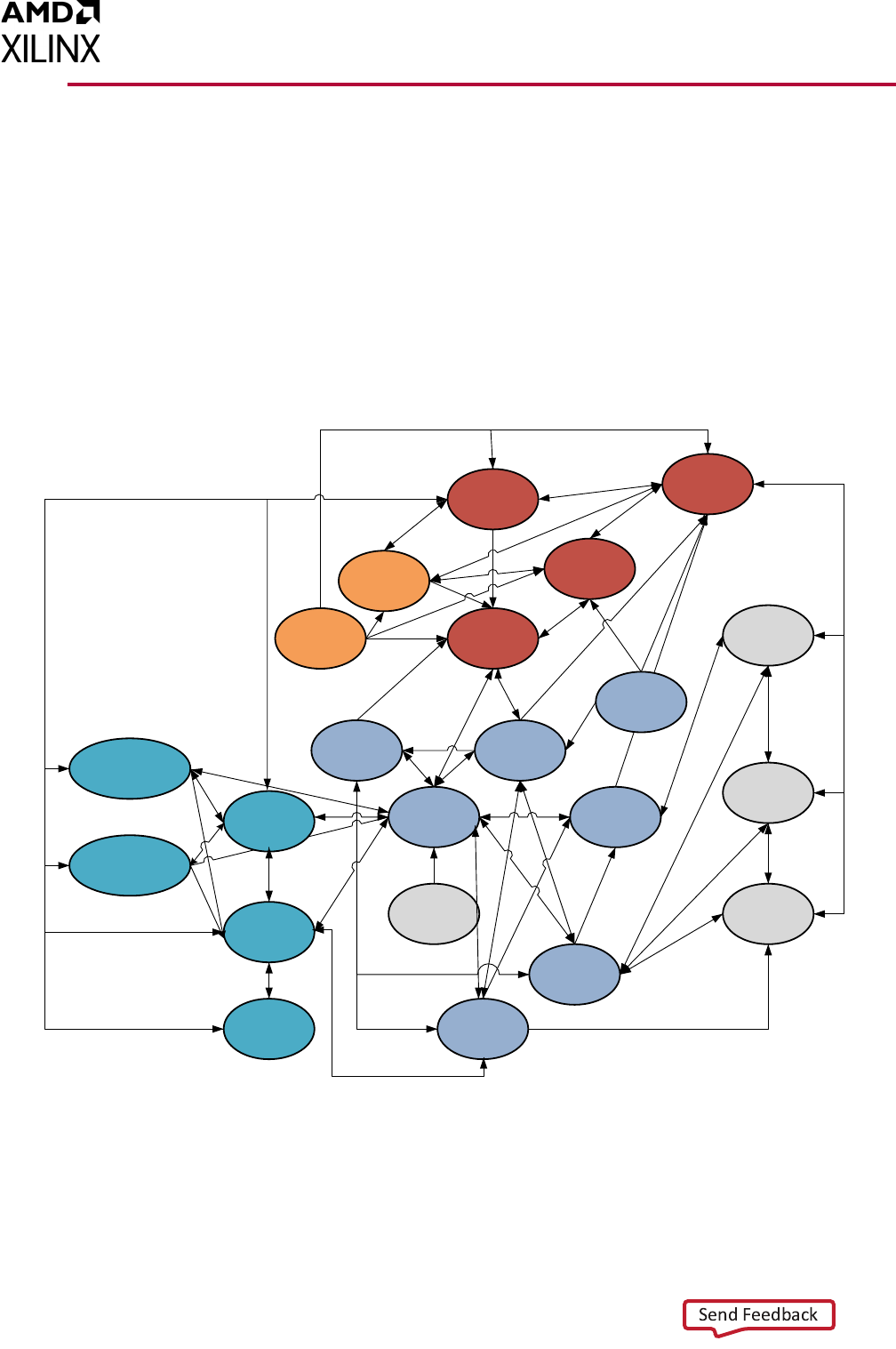
Netlist and Device Objects
Vivado Design Suite supports a number of first class objects in the in-memory design
database. These objects represent the cells, nets, and ports of the logical design, the device
resources of the target Xilinx device, or platform board, as well as objects used by specific
features of the Vivado Design Suite such as block design objects used by IP integrator, or
hardware objects used by the Vivado hardware manager. The Vivado Design Suite maps the
netlist objects of the logical design onto the device objects of the target device or board.
Figure 1-1, page 10 illustrates the relationships between some of the Vivado tools first class
objects. This figure is representative, and is not intended to depict all Vivado tools first class
objects, or their relationships.
The netlist objects, displayed at the top of Figure 1-1, are part of the logical design for
programming into the FPGA. Device objects, shown in the lower half of the figure, are part
of the actual physical device, and include area resources such as clock regions, tiles, sites or
X-Ref Target - Fig ure 1-1
Figure1‐1: Netlist and Device Objects
Net
Pin
Port
Clock
Cell
Bel
Site/CLB
Clock
Region
Package
Pin
Bel Pin
Site Pin
Site Pip
I/O
Standard
I/O Bank
Wire
Node
Pip
Tile
Timing
Path
SLR
PkgPin
_ByteGroup
PkgPin
_Nibble
X14826-071619

Vivado Properties Reference 11
UG912 (v2022.1) June 8, 2022 www.xilinx.com
Chapter1: Vivado Design Suite First Class Objects
CLBs. Device objects also include package pins and I/O banks, shown on the left side of the
figure, and routing resources such as nodes, wires, and pips, shown on the right in the
figure.
Additional categories of first class objects exist in the Vivado Design Suite, such as timing
objects, which combine with the netlist design to create timing reports and constrain
placement and routing results. Timing objects associated with the netlist and device
objects, provide a complete timing analysis of the implemented design. Timing objects
include clocks, timing paths, and delay objects.
The relationship between objects is shown by the arrows connecting two objects:
• A double headed arrow indicates that the relationship can be queried from either
direction. For instance, you can query the cells attached to specific nets (get_cells
-of_objects [get_nets]), or query the nets connected to specific cells
(get_nets -of_objects [get_cells]).
• A single-ended arrow reflects a relationship that can only be queried in the direction of
the arrow. For instance, in Figure 1-1, you can see that you can query the bels located
in specific clock regions (get_bels -of_objects [get_clock_regions]), but
you cannot get clock regions associated with specific bels.
A description of first class objects, their relationships to other objects, and the properties
defined on those objects follows.
Netlist Objects
• CELL, page 43
• CLOCK, page 47
• NET, page 108
• PIN, page 116
• PORT, page 126
• TIMING_PATH, page 139
Device Resource Objects
• BEL, page 37
• BEL_PIN, page 41
• CLOCK_REGION, page 50
• IO_BANK, page 104
• IO_STANDARD, page 106
• NODE, page 112


Vivado Properties Reference 13
UG912 (v2022.1) June 8, 2022 www.xilinx.com
Chapter1: Vivado Design Suite First Class Objects
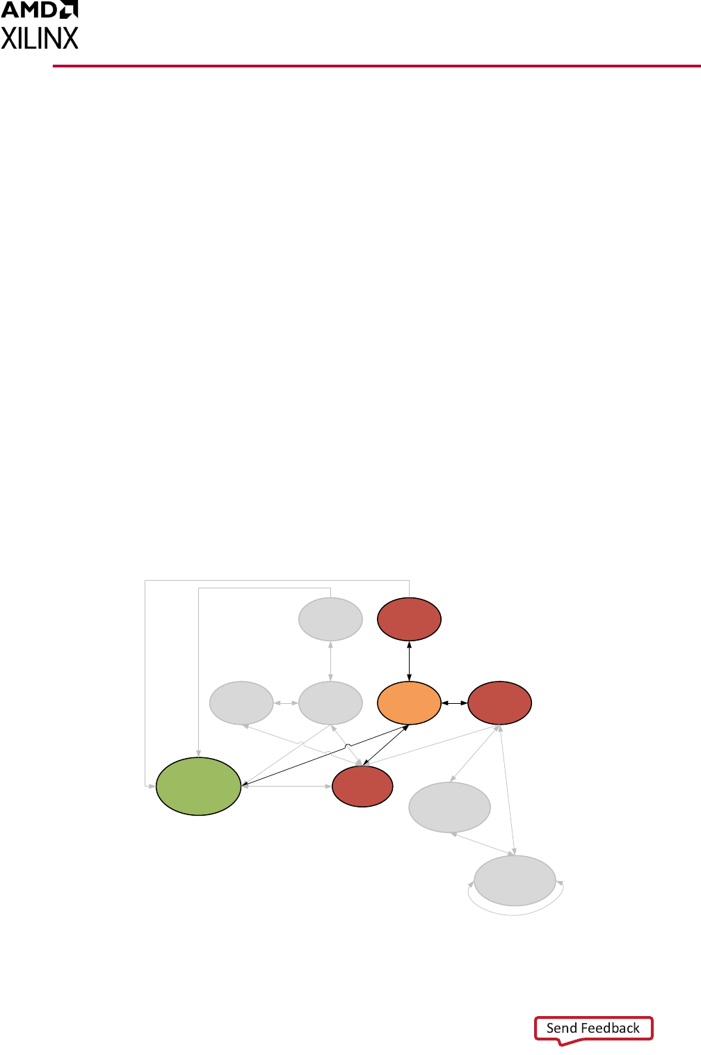
Block Design Objects
Block Designs are complex subsystem designs made up of interconnected IP cores, that can
either serve as stand-alone designs, or be integrated into other designs. Block Designs, or
diagrams, can be created with the IP integrator of the Vivado Design Suite. They can be
created interactively, on the canvas of the IP integrator in the Vivado Design Suite IDE, or
interactively using Tcl commands.
The Block Design diagram objects are structurally very similar to the netlist objects
previously described. The relationships between the different design objects that make up
Block Designs, or diagrams, are illustrated in Figure 1-2.
As seen in the figure above, the block diagram objects include:
• DIAGRAM, page 53
• BD_ADDR_SPACE, page 20
• BD_ADDR_SEG, page 17
X-Ref Target - Fig ure 1-2
Figure1‐2: Block Design Objects
bd_cell
bd_intf_pin
bd_intf_port
bd_intf_net
bd_port
bd_pin bd_net
diagram
bd_addr_space
bd_addr_seg
X14843-081315


Vivado Properties Reference 15
UG912 (v2022.1) June 8, 2022 www.xilinx.com
Chapter1: Vivado Design Suite First Class Objects
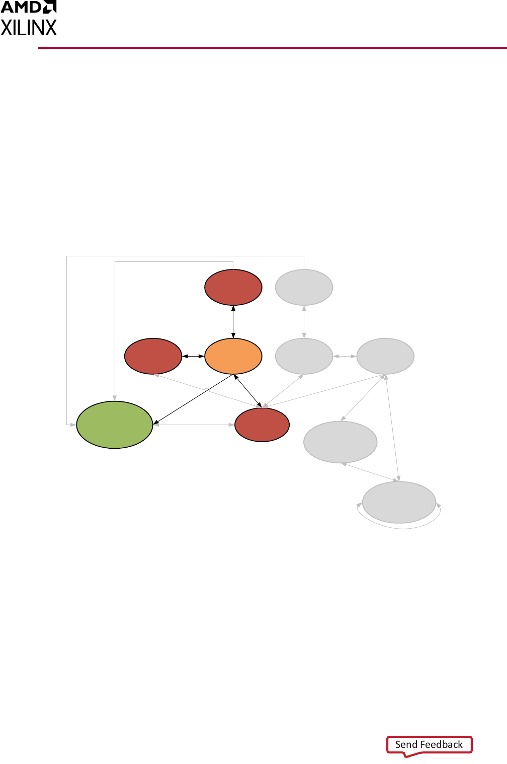
Hardware Manager Objects
The Hardware Manager is a feature of the Vivado Design Suite that lets you connect to a
device programmer or debug board, and exercise the programmed hardware device. The
Hardware Manager lets you exercise debug logic on devices, accessing signals to set or
retrieve current values. The many debug cores and objects of the Vivado hardware manager
are shown in Figure 1-3.
Debug cores can be instantiated into an RTL design from the Xilinx IP catalog, or in the case
of the ILA or VIO debug cores, can be inserted into the synthesized netlist using the
netlist-based debug flow. Refer to Vivado Design Suite User Guide: Programming and
Debugging (UG908) [Ref 23] for more information.
As seen in the figure above, the Vivado hardware manager objects include:
• HW_AXI, page 54
• HW_BITSTREAM, page 56
• HW_CFGMEM, page 58
X-Ref Target - Fig ure 1-3
Figure1‐3: Hardware Manager Objects
hw_server
hw_vio
hw_target hw_device
hw_ilahw_sysmon
hw_sio_ibert
hw_axi
hw_probe
hw_ila_data
hw_bitstream
hw_cfgmem
hw_axi_txn
hw_sio_gtgroup
hw_sio_gt
hw_sio_tx hw_sio_rx
hw_sio_pll
hw_sio_sca
n
hw_sio_sweep
hw_sio_link
hw_sio_linkgroup
hw_sysmon_reg
X14844-081315

Vivado Properties Reference 16
UG912 (v2022.1) June 8, 2022 www.xilinx.com
Chapter1: Vivado Design Suite First Class Objects
• HW_DEVICE, page 60
• HW_ILA, page 63
• HW_ILA_DATA, page 66
• HW_PROBE, page 67
• HW_SERVER, page 70
• HW_SIO_GT, page 71
• HW_SIO_GTGROUP, page 81
• HW_SIO_IBERT, page 82
• HW_SIO_PLL, page 84
• HW_SIO_RX, page 86
• HW_SIO_TX, page 92
• HW_SYSMON, page 96
• HW_TARGET, page 100
• HW_VIO, page 102

Vivado Properties Reference 17
UG912 (v2022.1) June 8, 2022 www.xilinx.com
Chapter 2
Alphabetical List of First Class Objects
BD_ADDR_SEG
Description
Address segments, or bd_addr_seg objects, describe the location and size of a range of
memory. They have a range (size) and an optional starting offset.
For various memory mapped master and slave interfaces, IP integrator follows the industry
standard IP-XACT data format for capturing memory requirements and capabilities of
endpoint masters and slaves.
Addressable slave interfaces reference an address segment container, called a memory
map. These memory maps are usually named after the slave interface pins, for example
S_AXI, though that is not required.
The memory map contains slave address segments. These address segments correspond to
the address decode window for the slave interface referencing the memory map. When
specified in the memory map, slave segments must have a range and can optionally have a
hard offset, (indicating that the slave can only be mapped into master address spaces at
that offset or apertures of it).
A typical AXI4-Lite slave interface for instance references a memory map with only one
address segment, representing a range of memory. However, some slaves, like a bridge, will
have multiple address segments; or a range of addresses for each address decode window.
Slave address segments are assigned into master address spaces using the
assign_bd_address or create_bd_addr_seg command.
Addressing master interfaces reference an address segment container called an Address
Space, or bd_addr_space. The address space is referenced by interface pins, bd_intf_pin, on
the cell. In the case of external AXI masters, the address space is referenced by the external
interface port, bd_intf_port. Several interfaces of varying protocols can reference the same
master address space. The Microblaze processor Data address space, for instance, is
referenced by its DLMB, M_AXI_DP and M_AXI_DC interfaces.

Vivado Properties Reference 18
UG912 (v2022.1) June 8, 2022 www.xilinx.com
Chapter2: Alphabetical List of First Class Objects
The Address space contains master address segments. These master address segments
reference slave address segments that have been assigned into the master address space,
and the offset and range at which the master accesses it.
Related Objects
The bd_addr_seg object refers to both master and slave address segments. The
bd_addr_space object refers to both memory maps and master address spaces.
You can query the relationship between all related address spaces and address segments.
For example:
# Get the slave address segments of a memory map space.
get_bd_addr_segs -of_objects [get_bd_addr_spaces /mdm_1/S_AXI]
# Get the master address segments of amaster address space.
get_bd_addr_segs -of_objects [get_bd_addr_spaces /Microblaze_0/Data]
# Get the slave adress segment from its referenced master address segment, or the
# master address segment from its referencing slave address segment.
get_bd_addr_segs -of_objects [get_bd_addr_segs <slave or master>_segment]
# Get the addr_segs referencing/referenced by interfaces.
X-Ref Target - Fig ure 2-1
Figure2‐1: Block Design Address Space and Address Segments
bd_cell
bd_intf_pin
bd_intf_port
bd_intf_net
bd_port
bd_pin bd_net
diagram
bd_addr_space
bd_addr_seg
X14845-081315

Vivado Properties Reference 19
UG912 (v2022.1) June 8, 2022 www.xilinx.com
Chapter2: Alphabetical List of First Class Objects
# Get all Master or slave interfaces.
set vMB [get_bd_intf_pins -of_objects [get_bd_cells *] -filter {Mode == "Master"}]
set vSB [get_bd_intf_pins -of_objects [get_bd_cells *] -filter {Mode == "Slave"}]
# Get master segments
set vMS [get_bd_addr_segs -of_objects $vMB]
# Get slave segments
set vSS [get_bd_addr_segs -of_objects $vSB]
Properties
The properties on a block design address segment object, bd_addr_seg, include the
following, with example values:
Property Type Read-only Visible Value
ACCESS string false true read-write
CLASS string true true bd_addr_seg
EXEIMG string false true
MEMTYPE string false true data
NAME string false true SEG_axi_gpio_0_Reg
OFFSET string false true 0x40000000
PATH string true true /microblaze_0/Data/SEG_axi_gpio_0_Reg
RANGE string false true 0x00010000
SECURE bool false true 0
USAGE string false true register
To report the properties for a bd_addr_seg object, you can copy and paste the following
command into the Vivado Design Suite Tcl shell or Tcl Console:
report_property -all [lindex [get_bd_addr_segs ] 0]

Vivado Properties Reference 20
UG912 (v2022.1) June 8, 2022 www.xilinx.com
Chapter2: Alphabetical List of First Class Objects
BD_ADDR_SPACE
Description
An address space, or bd_addr_space object, is an assigned logically addressable space of
memory on a master interface, or on AXI interface ports connected to an AXI master
external to the block design.
The IP integrator of the Vivado Design Suite follows the industry standard IP-XACT data
format for capturing memory requirements and capabilities. Some blocks can have one
address space associated with multiple master interfaces, for example a processor with a
system bus and fast memory bus. Other components can have multiple address spaces
associated with multiple master interfaces, one for instruction and the other for data.
Master interfaces reference address spaces, or bd_addr_space objects. When an AXI slave is
mapped to a master address space, a master address segment (bd_addr_seg) object is
created, mapping the address segments of the slave to the master.
Related Objects
X-Ref Target - Fig ure 2-2
Figure2‐2: Block Design Address Space and Address Segments
bd_cell
bd_intf_pin
bd_intf_port
bd_intf_net
bd_port
bd_pin bd_net
diagram
bd_addr_space
bd_addr_seg
X14845-081315

Vivado Properties Reference 21
UG912 (v2022.1) June 8, 2022 www.xilinx.com
Chapter2: Alphabetical List of First Class Objects
The master address segment, bd_addr_seg, is associated with the address spaces in AXI
master interfaces, found on a block design. The address space is referenced by the interface
pins, bd_intf_pin, on the cell, bd_cell. External AXI masters are associated with interface
ports, bd_intf_port.
You can query the bd_addr_space objects of these associated objects:
get_bd_addr_spaces -of_objects [get_bd_cells /microblaze_0]
get_bd_addr_segs -of_objects [get_bd_addr_spaces -of_objects [get_bd_cells
/microblaze_0]]
You can also query the objects associated with the block design address spaces:
get_bd_intf_pins -of_objects [get_bd_addr_spaces *SLMB]
Properties
The properties on a block design address space object, bd_addr_space, include the
following, with example values:
Property Type Read-only Visible Value
CLASS string true true bd_addr_space
NAME string false true Data
OFFSET string false true 0x00000000
PATH string true true /microblaze_0/Data
RANGE string false true 0x100000000
TYPE string false true
To report the properties for a bd_addr_space object, you can copy and paste the following
command into the Vivado Design Suite Tcl shell or Tcl Console:
report_property -all [lindex [get_bd_addr_spaces ] 0]

Vivado Properties Reference 22
UG912 (v2022.1) June 8, 2022 www.xilinx.com
Chapter2: Alphabetical List of First Class Objects
BD_CELL
Description
A block design cell, or bd_cell object, is an instance of an IP integrator IP core object, or is
a hierarchical block design cell. A leaf-cell is a core from the IP catalog. A hierarchical cell is
a module or block that contains one or more additional levels of logic, including leaf-cells.
The TYPE property of the bd_cell object identifies the block design cell as either a lead-cell
coming from the IP catalog (TYPE == IP), or as a hierarchical module containing additional
logic (TYPE == HIER).
Related Objects
As seen in Figure 2-3, Block design cells (bd_cell) are found in a block design, or diagram
object. The cells include block design pins (bd_pin) and interface pins (bd_intf_pin), and can
hierarchically contain block design ports (bd_port) and interface ports (bd_intf_port). They
are connected by nets (bd_net) and interface nets (bd_intf_net). Memory related block
design cells can also contain address spaces (bd_addr_space), and address segments
(bd_addr_seg). You can query the block design cells that are associated with any of these
objects, for example:
X-Ref Target - Fig ure 2-3
Figure2‐3: Block Design Cells
bd_cell
bd_intf_pin
bd_intf_port
bd_intf_net
bd_port
bd_pin bd_net
diagram
bd_addr_space
bd_addr_seg
X14846-081315

Vivado Properties Reference 23
UG912 (v2022.1) June 8, 2022 www.xilinx.com
Chapter2: Alphabetical List of First Class Objects
get_bd_cells -of_objects [get_bd_addr_spaces]
You can query the objects associated with block design cells:
get_bd_addr_spaces -of_objects [get_bd_cells]
You can also query the block design cells that are hierarchically objects of another block
design cell:
get_bd_cells -of_objects [get_bd_cells microblaze_0_axi_periph]
Properties
The specific properties on a block design cell object can be numerous and varied,
depending on the type of IP core the object represents. The following table lists some of the
properties assigned to a bd_cell object in the Vivado Design Suite, with example values:
Property Type Read-only Visible Value
CLASS string true true bd_cell
CONFIG.C_ALL_INPUTS string false true 0
CONFIG.C_ALL_INPUTS_2 string false true 0
CONFIG.C_ALL_OUTPUTS string false true 1
CONFIG.C_ALL_OUTPUTS_2 string false true 0
CONFIG.C_DOUT_DEFAULT string false true 0x00000000
CONFIG.C_DOUT_DEFAULT_2 string false true 0x00000000
CONFIG.C_GPIO2_WIDTH string false true 32
CONFIG.C_GPIO_WIDTH string false true 4
CONFIG.C_INTERRUPT_PRESENT string false true 0
CONFIG.C_IS_DUAL string false true 0
CONFIG.C_TRI_DEFAULT string false true 0xFFFFFFFF
CONFIG.C_TRI_DEFAULT_2 string false true 0xFFFFFFFF
CONFIG.Component_Name string false true base_mb_axi_gpio_0_0
CONFIG.GPIO2_BOARD_INTERFACE string false true Custom
CONFIG.GPIO_BOARD_INTERFACE string false true led_4bits
CONFIG.USE_BOARD_FLOW string false true true
LOCATION string false true 5 1720 200
LOCK_UPGRADE bool false true 0
NAME string false true axi_gpio_0
PATH string true true /axi_gpio_0
SCREENSIZE string false true 180 116
SDX_KERNEL string true false false
SDX_KERNEL_SIM_INST string true false
SDX_KERNEL_SYNTH_INST string true false
SDX_KERNEL_TYPE string true false
SELECTED_SIM_MODEL string false true rtl
TYPE string true true ip
VLNV string true true xilinx.com:ip:axi_gpio:2.0
To report the properties for a bd_cell object, you can copy and paste the following
command into the Vivado Design Suite Tcl shell or Tcl Console:
report_property -all [lindex [get_bd_cells] 0]
Vivado Properties Reference 24
UG912 (v2022.1) June 8, 2022 www.xilinx.com
Chapter2: Alphabetical List of First Class Objects
BD_INTF_NET
Description
An interface is a grouping of signals that share a common function, containing both
individual signals and multiple buses. An AXI4-Lite master, for example, contains a large
number of individual signals plus multiple buses, which are all required to make a
connection. By grouping these signals and buses into an interface, the Vivado IP integrator
can identify common interfaces and automatically make multiple connections in a single
step.
An interface is defined using the IP-XACT standard. Standard interfaces provided by Xilinx
can be found in the Vivado tools installation directory at data/ip/interfaces. See the Vivado
Design Suite User Guide: Designing IP Subsystems Using IP Integrator (UG994) [Ref 27] for
more information on interface nets, pins, and ports.
A block design interface net, or a bd_intf_net object, connects the interface pins on a block
design cell to other interface pins, or to external interface ports. The bd_intf_net object
connects through multiple levels of the design hierarchy, connecting block design cells.
Every interface net has a name which identifies it in the design. All block design cells,
interface pins, and interface ports connected to these nets are electrically connected.
Related Objects
X-Ref Target - Fig ure 2-4
Figure2‐4: Block Design Interface Nets
bd_cell
bd_intf_pin
bd_intf_port
bd_intf_net
bd_port
bd_pin bd_net
diagram
bd_addr_space
bd_addr_seg
X14847-081315

Vivado Properties Reference 25
UG912 (v2022.1) June 8, 2022 www.xilinx.com
Chapter2: Alphabetical List of First Class Objects
As seen in Figure 2-4, page 24, the block design interface net, bd_intf_net object, occurs
in a block design, or diagram. It is connected to interface ports (bd_intf_port), and
through interface pins (bd_intf_pin) to block design cells (bd_cell) in the diagram. You
can query the bd_intf_nets of the diagram, bd_cell, bd_intf_pin, and bd_intf_port objects.
get_bd_intf_nets -of_objects [get_bd_ports]
In addition, you can query the block design cells (bd_cell) or the bd_intf_pins or
bd_intf_port objects that are connected to a specific bd_intf_net:
get_bd_cells -of_objects [get_bd_intf_nets /INTERRUPT_1_1]
Properties
The properties on the bd_intf_net object include the following:
Property Type Read-only Visible Value
CLASS string true true bd_intf_net
NAME string false true microblaze_0_axi_periph_to_s00_couplers
PATH string true true
/microblaze_0_axi_periph/microblaze_0_axi_periph_to_s00_couplers
To report the properties for the bd_intf_net object, you can copy and paste the following
command into the Vivado Design Suite Tcl shell or Tcl Console:
report_property -all [lindex [get_bd_intf_nets] 0]

Vivado Properties Reference 26
UG912 (v2022.1) June 8, 2022 www.xilinx.com
Chapter2: Alphabetical List of First Class Objects
BD_INTF_PIN
Description
An interface is a grouping of signals that share a common function, containing both
individual signals and multiple buses. An AXI4-Lite master, for example, contains a large
number of individual signals plus multiple buses, which are all required to make a
connection. By grouping these signals and buses into an interface, the Vivado IP integrator
can identify common interfaces and automatically make multiple connections in a single
step.
An interface is defined using the IP-XACT standard. Standard interfaces provided by Xilinx
can be found in the Vivado tools installation directory at data/ip/interfaces. See the Vivado
Design Suite User Guide: Designing IP Subsystems Using IP Integrator (UG994) [Ref 27] for
more information on interface nets, pins, and ports.
A block design interface pin, or a bd_intf_pin object, is a point of logical connectivity on a
block design cell. An interface pin allows the internals of a cell to be abstracted away and
simplified for ease-of-use. Interface pins can appear on hierarchical block design cells, or
leaf-level cells.
Related Objects
X-Ref Target - Fig ure 2-5
Figure2‐5: Block Design Interface Pin
bd_cell
bd_intf_pin
bd_intf_port
bd_intf_net
bd_port
bd_pin bd_net
diagram
bd_addr_space
bd_addr_seg
X14848-081315

Vivado Properties Reference 27
UG912 (v2022.1) June 8, 2022 www.xilinx.com
Chapter2: Alphabetical List of First Class Objects
A block design interface pin is attached to a block design cell (bd_cell), and can be
connected to other interface pins (bd_intf_pin) or interface ports (bd_intf_port) by an
interface net (bd_intf_net) in the block design, or diagram.
You can query the bd_intf_pins of bd_addr_space, bd_addr_seg, bd_cell, and bd_intf_net
objects:
get_bd_intf_pins -of_objects [get_bd_cells clk_wiz_1]
You can also query the bd_addr_spaces, bd_addr_segs, bd_cells, and bd_intf_nets, of a
specific bd_intf_pin:
get_bd_addr_spaces -of_objects [get_bd_intf_pins microblaze_0/*]
Properties
The specific properties on a block design interface pin object can vary depending on the
type of the pin. The following table lists some of the properties assigned to a master AXI
interface pin object, with example values:
Property Type Read-only Visible Value
BRIDGES string false false
CLASS string true true bd_intf_pin
CONFIG.ADDR_WIDTH string true true 32
CONFIG.ARUSER_WIDTH string true true 0
CONFIG.AWUSER_WIDTH string true true 0
CONFIG.BUSER_WIDTH string true true 0
CONFIG.CLK_DOMAIN string true true base_mb_clk_wiz_1_0_clk_out1
CONFIG.DATA_WIDTH string true true 32
CONFIG.FREQ_HZ string true true 100000000
CONFIG.HAS_BRESP string true true 1
CONFIG.HAS_BURST string true true 0
CONFIG.HAS_CACHE string true true 0
CONFIG.HAS_LOCK string true true 0
CONFIG.HAS_PROT string true true 1
CONFIG.HAS_QOS string true true 0
CONFIG.HAS_REGION string true true 0
CONFIG.HAS_RRESP string true true 1
CONFIG.HAS_WSTRB string true true 1
CONFIG.ID_WIDTH string true true 0
CONFIG.MAX_BURST_LENGTH string true true 1
CONFIG.NUM_READ_OUTSTANDING string true true 1
CONFIG.NUM_READ_THREADS string true true 1
CONFIG.NUM_WRITE_OUTSTANDING string true true 1
CONFIG.NUM_WRITE_THREADS string true true 1
CONFIG.PHASE string true true 0.0
CONFIG.PROTOCOL string true true AXI4LITE
CONFIG.READ_WRITE_MODE string true true READ_WRITE
CONFIG.RUSER_BITS_PER_BYTE string true true 0
CONFIG.RUSER_WIDTH string true true 0
CONFIG.SUPPORTS_NARROW_BURST string true true 0
CONFIG.WUSER_BITS_PER_BYTE string true true 0
CONFIG.WUSER_WIDTH string true true 0
LOCATION string false true
MODE string true true Master

Vivado Properties Reference 28
UG912 (v2022.1) June 8, 2022 www.xilinx.com
Chapter2: Alphabetical List of First Class Objects
NAME string false true M_AXI_DP
PATH string true true /microblaze_0/M_AXI_DP
TYPE string true true ip
VLNV string true true
xilinx.com:interface:aximm_rtl:1.0
To report the properties for the bd_intf_pin object, you can copy and paste the following
command into the Vivado Design Suite Tcl shell or Tcl Console:
report_property -all [lindex [get_bd_intf_pins */*] 0]
Or use the following Tcl script to report the properties of each bd_intf_pin object on each
block design cell:
foreach x [get_bd_intf_pins -of_objects [get_bd_cells]] {
puts "Next Interface Pin starts here
..............................................."
report_property -all $x
}

Vivado Properties Reference 29
UG912 (v2022.1) June 8, 2022 www.xilinx.com
Chapter2: Alphabetical List of First Class Objects
BD_INTF_PORT
Description
An interface is a grouping of signals that share a common function, containing both
individual signals and multiple buses. An AXI4-Lite master, for example, contains a large
number of individual signals plus multiple buses, which are all required to make a
connection. By grouping these signals and buses into an interface, the Vivado IP integrator
can identify common interfaces and automatically make multiple connections in a single
step.
An interface is defined using the IP-XACT standard. Standard interfaces provided by Xilinx
can be found in the Vivado tools installation directory at data/ip/interfaces. See the Vivado
Design Suite User Guide: Designing IP Subsystems Using IP Integrator (UG994) [Ref 27] for
more information on interface nets, pins, and ports.
A block design interface port is a special type of hierarchical pin, a pin on the top-level of
the block diagram. In block designs, ports and interface are primary ports communicating
the external connection of the block design or diagram from or to the overall FPGA design,
or system level design.
Related Objects
X-Ref Target - Fig ure 2-6
Figure2‐6: Block Design Interface Port
bd_cell
bd_intf_pin
bd_intf_port
bd_intf_net
bd_port
bd_pin bd_net
diagram
bd_addr_space
bd_addr_seg
X14849-081315

Vivado Properties Reference 30
UG912 (v2022.1) June 8, 2022 www.xilinx.com
Chapter2: Alphabetical List of First Class Objects
The block design interface port, bd_intf_port object, occurs in a block design, or diagram. It
is connected by block design interface nets (bd_intf_net) to the pins of block design cells
(bd_cell). You can query the bd_intf_ports of the diagram, or those connected to block
design interface nets.
get_bd_intf_ports -of_objects [get_bd_intf_nets]
You can also query the interface nets connected to bd_intf_port objects:
get_bd_intf_nets -of_objects [get_bd_intf_ports CLK*]
Properties
The specific properties on a block design interface port object can vary depending on the
type of the port. The following table lists some of the properties assigned to a clock
bd_intf_port object, with example values:
Property Type Read-only Visible Value
CLASS string true true bd_intf_port
LOCATION string false true 1950 430
MODE string true true Master
NAME string false true ddr4_sdram
PATH string true true /ddr4_sdram
VLNV string true true xilinx.com:interface:ddr4_rtl:1.0
To report the properties for a bd_intf_port object, you can copy and paste the following
command into the Vivado Design Suite Tcl shell or Tcl Console:
report_property -all [lindex [get_bd_intf_ports] 0]
Vivado Properties Reference 31
UG912 (v2022.1) June 8, 2022 www.xilinx.com
Chapter2: Alphabetical List of First Class Objects
BD_NET
Description
A block design net, or a bd_net object, connects the pins on an IP integrator block design
cell to other pins, or to external ports. The bd_net object connects through multiple levels
of the design hierarchy, connecting block design cells. Every net has a name which
identifies it in the design. All block design cells, pins, and ports connected to these nets are
electrically connected.
Related Objects
The block design net, bd_net object, occurs in a block design, or diagram. It is connected to
ports (bd_port), and through pins (bd_pin) to block design cells (bd_cell) in the diagram.
You can query the bd_nets of the diagram, bd_cell, bd_pin, and bd_port objects.
get_bd_nets -of_objects [get_bd_ports]
In addition, you can query the bd_cells, or the bd_pins, or bd_port objects that are
connected to a specific bd_net:
get_bd_cells -of_objects [get_bd_nets clk_wiz*]
X-Ref Target - Fig ure 2-7
Figure2‐7: Block Design Nets
bd_cell
bd_intf_pin
bd_intf_port
bd_intf_net
bd_port
bd_pin bd_net
diagram
bd_addr_space
bd_addr_seg
X14850-081315

Vivado Properties Reference 32
UG912 (v2022.1) June 8, 2022 www.xilinx.com
Chapter2: Alphabetical List of First Class Objects
Properties
The properties on the bd_net object include the following:
Property Type Read-only Visible Value
CLASS string true true bd_net
NAME string false true clk_wiz_1_locked
PATH string true true /clk_wiz_1_locked
To report the properties for the bd_net object, you can copy and paste the following
command into the Vivado Design Suite Tcl shell or Tcl Console:
report_property -all [lindex [get_bd_nets] 0]

Vivado Properties Reference 33
UG912 (v2022.1) June 8, 2022 www.xilinx.com
Chapter2: Alphabetical List of First Class Objects
BD_PIN
Description
A block design pin, or a bd_pin object, is a point of logical connectivity on a block design
cell. A block design pin allows the internal logic of a cell to be abstracted away and
simplified for ease-of-use. Pins can be scalar or bus pins, and can appear on hierarchical
block design cells, or leaf-level cells.
Related Objects
As seen in Figure 2-8, a block design pin is attached to a block design cell (bd_cell), and can
be connected to other pins or ports by a net (bd_net) in the block design, or diagram.
You can query the bd_pins of bd_cell and bd_net objects:
get_bd_pins -of_objects [get_bd_cells clk_wiz_1]
In addition, you can query the bd_cell, or the bd_net, of a specific bd_pin:
get_bd_cells -of [get_bd_pins */Reset]
X-Ref Target - Fig ure 2-8
Figure2‐8: Block Design Pins
bd_cell
bd_intf_pin
bd_intf_port
bd_intf_net
bd_port
bd_pin bd_net
diagram
bd_addr_space
bd_addr_seg
X14851-081315

Vivado Properties Reference 34
UG912 (v2022.1) June 8, 2022 www.xilinx.com
Chapter2: Alphabetical List of First Class Objects
Properties
The specific properties on a block design pin object can vary depending on the type of the
pin. The following table lists some of the properties assigned to a CLK type bd_pin object in
the Vivado Design Suite, with example values:
Property Type Read-only Visible Value
CLASS string true true bd_pin
DEFAULT_DRIVER string true true 0000
DIR string true true O
INTF string true true TRUE
LEFT string true true 3
LOCATION string false true
NAME string false true gpio_io_o
PATH string true true /axi_gpio_0/gpio_io_o
RIGHT string true true 0
TYPE string true true undef
To report the properties for the bd_net object, you can copy and paste the following
command into the Vivado Design Suite Tcl shell or Tcl Console:
report_property -all [lindex [get_bd_pins */*] 0]

Vivado Properties Reference 35
UG912 (v2022.1) June 8, 2022 www.xilinx.com
Chapter2: Alphabetical List of First Class Objects
BD_PORT
Description
A block design port is a special type of hierarchical pin, a pin on the top-level diagram. In
block designs, the ports are primary ports communicating the external connection of the
block design or diagram to the overall FPGA design, or system-level design.
Related Objects
The block design port, bd_port object, occurs in a block design, or diagram. It is connected
by block design nets (bd_net) to the pins (bd_pin) of block design cells (bd_cell) in the
diagram. You can query the bd_ports of the diagram, or those connected to block design
nets.
get_bd_ports -of_objects [get_bd_nets]
You can also query the block design nets connected to bd_port objects:
get_bd_nets -of_objects [get_bd_ports aux_reset_in]
X-Ref Target - Fig ure 2-9
Figure2‐9: Block Design Port
bd_cell
bd_intf_pin
bd_intf_port
bd_intf_net
bd_port
bd_pin bd_net
diagram
bd_addr_space
bd_addr_seg
X14852-081315

Vivado Properties Reference 36
UG912 (v2022.1) June 8, 2022 www.xilinx.com
Chapter2: Alphabetical List of First Class Objects
Properties
The specific properties on a block design port object can vary depending on the type of the
port. The following table lists some of the properties assigned to a RESET type bd_port
object in the Vivado Design Suite, with example values:
Property Type Read-only Visible Value
CLASS string true true bd_port
CONFIG.POLARITY string false true ACTIVE_LOW
DIR string true true I
INTF string true true FALSE
LEFT string false true
LOCATION string false true 130 560
NAME string false true aux_reset_in
PATH string true true /aux_reset_in
RIGHT string false true
TYPE string true true rst
To report the properties for a bd_port object, you can copy and paste the following
command into the Vivado Design Suite Tcl shell or Tcl Console:
report_property -all [lindex [get_bd_ports] 0]

Vivado Properties Reference 37
UG912 (v2022.1) June 8, 2022 www.xilinx.com
Chapter2: Alphabetical List of First Class Objects
BEL
Description
Typically a BEL, or Basic Element, corresponds to leaf-cell in the netlist view of the design.
BELs are device objects on the target Xilinx FPGA on which to place, or map, basic netlist
objects like flip-flops, LUTs, and carry logic.
BELs are grouped together on the device in SITE objects, such as SLICEs and IO Blocks
(IOBs). One or more BELs can be located in a single SITE, and you can use the BEL to assign
logic from the design netlist into specific locations or device resources on the target device.
There are a number of different bel types available on the different Xilinx FPGAs. The
following are the types of bels found on the Kintex
®
-7 part, xc7k70tfbg676. The different
TYPEs of BELs are enumerated below:
AFF AFF2
BFF BFF2
BITSLICE_CONTROL_BEL
BSCAN1 BSCAN2 BSCAN3 BSCAN4 BSCAN_BSCAN
BUFCE_BUFCE BUFCE_BUFCE_LEAF BUFCE_BUFCE_ROW
BUFFER
BUFGCE_DIV_BUFGCE_DIV BUFGCTRL_BUFGCTRL BUFG_GT_BUFG_GT BUFG_GT_BUFG_GT_SYNC
BUFHCE_BUFHCE BUFIO_BUFIO BUFMRCE_BUFMRCE BUFR_BUFR
CAPTURE_CAPTURE
CARRY4 CARRY8
CFF CFF2
CFG_IO_ACCESS
DCIRESET DCIRESET_DCIRESET
DFF DFF2
DNA_PORT DNA_PORT_DNA_PORT
DSP48E1_DSP48E1 DSP_ALU DSP_A_B_DATA DSP_C_DATA DSP_MULTIPLIER DSP_M_DATA
DSP_OUTPUT DSP_PREADD DSP_PREADD_DATA
EFF EFF2
EFUSE_USR EFUSE_USR_EFUSE_USR
F7MUX F8MUX F9MUX
FFF FFF2
FF_INIT
FIFO18E1_FIFO18E1
FRAME_ECC FRAME_ECC_FRAME_ECC
GCLK_DELAY
GFF GFF2
GTHE3_CHANNEL_GTHE3_CHANNEL
GTHE3_CHANNEL_IPAD1 GTHE3_CHANNEL_IPAD2
GTHE3_CHANNEL_OPAD1 GTHE3_CHANNEL_OPAD2
GTHE3_COMMON_GTHE3_COMMON
GTHE3_COMMON_PADN GTHE3_COMMON_PADP
GTXE2_CHANNEL_GTXE2_CHANNEL GTXE2_COMMON_GTXE2_COMMON
HARD0 HARD1
HARD_SYNC_SYNC_UNIT
HFF HFF2
HPIOBDIFFINBUF_DIFFINBUF HPIOBDIFFOUTBUF_DIFFOUTBUF
HPIOB_IBUFCTRL

Vivado Properties Reference 38
UG912 (v2022.1) June 8, 2022 www.xilinx.com
Chapter2: Alphabetical List of First Class Objects
HPIOB_INBUF HPIOB_OUTBUF
HPIOB_PAD HPIOB_PULL
HPIO_OUTINV HPIO_VREF
HRIODIFFINBUF_DIFFINBUF HRIODIFFOUTBUF_DIFFOUTBUF
HRIO_IBUFCTRL
HRIO_INBUF HRIO_OUTBUF
HRIO_OUTINV HRIO_PAD HRIO_PULL
IBUFDS0_GTE3 IBUFDS1_GTE3 IBUFDS_GTE2_IBUFDS_GTE2
ICAP_BOT ICAP_ICAP ICAP_TOP
IDELAYCTRL_IDELAYCTRL
IDELAYE2_FINEDELAY_IDELAYE2_FINEDELAY
IDELAYE2_IDELAYE2
ILOGICE2_IFF
ILOGICE3_IFF ILOGICE3_ZHOLD_DELAY
INVERTER
IN_FIFO_IN_FIFO
IOB18M_INBUF_DCIEN IOB18M_OUTBUF_DCIEN IOB18M_TERM_OVERRIDE
IOB18S_INBUF_DCIEN IOB18S_OUTBUF_DCIEN IOB18S_TERM_OVERRIDE
IOB18_INBUF_DCIEN IOB18_OUTBUF_DCIEN IOB18_TERM_OVERRIDE
IOB33M_INBUF_EN IOB33M_OUTBUF IOB33M_TERM_OVERRIDE
IOB33S_INBUF_EN IOB33S_OUTBUF IOB33S_TERM_OVERRIDE
IOB33_INBUF_EN IOB33_OUTBUF IOB33_TERM_OVERRIDE
LUT5 LUT6
LUT_OR_MEM5 LUT_OR_MEM6
MASTER_JTAG
MMCME2_ADV_MMCME2_ADV MMCME3_ADV_MMCM_TOP
OBUFDS0_GTE3 OBUFDS1_GTE3
ODELAYE2_ODELAYE2
OLOGICE2_MISR OLOGICE2_OUTFF OLOGICE2_TFF
OLOGICE3_MISR OLOGICE3_OUTFF OLOGICE3_TFF
OUT_FIFO_OUT_FIFO
PAD
PCIE_2_1_PCIE_2_1 PCIE_3_1_PCIE_3_1
PHASER_IN_PHY_PHASER_IN_PHY PHASER_OUT_PHY_PHASER_OUT_PHY
PHASER_REF_PHASER_REF
PHY_CONTROL_PHY_CONTROL
PLLE2_ADV_PLLE2_ADV PLLE3_ADV_PLL_TOP PLL_SELECT_BEL
PMV2_PMV2
PULL_OR_KEEP1
RAMB18E1_RAMB18E1 RAMB18E2_U_RAMB18E2 RAMBFIFO18E2_RAMBFIFO18E2
RAMBFIFO36E1_RAMBFIFO36E1 RAMBFIFO36E2_RAMBFIFO36E2
REG_INIT
RIU_OR_BEL
RXTX_BITSLICE
SELMUX2_1
SLICEL_A5LUT SLICEL_A6LUT
SLICEL_B5LUT SLICEL_B6LUT
SLICEL_C5LUT SLICEL_C6LUT
SLICEL_CARRY4_AMUX SLICEL_CARRY4_AXOR
SLICEL_CARRY4_BMUX SLICEL_CARRY4_BXOR
SLICEL_CARRY4_CMUX SLICEL_CARRY4_CXOR
SLICEL_CARRY4_DMUX SLICEL_CARRY4_DXOR
SLICEL_D5LUT SLICEL_D6LUT SLICEL_E5LUT
SLICEL_E6LUT SLICEL_F5LUT SLICEL_F6LUT
SLICEL_G5LUT SLICEL_G6LUT SLICEL_H5LUT
SLICEL_H6LUT SLICEM_A5LUT SLICEM_A6LUT
SLICEM_B5LUT SLICEM_B6LUT SLICEM_C5LUT
SLICEM_C6LUT SLICEM_CARRY4_AMUX SLICEM_CARRY4_AXOR
SLICEM_CARRY4_BMUX SLICEM_CARRY4_BXOR

Vivado Properties Reference 39
UG912 (v2022.1) June 8, 2022 www.xilinx.com
Chapter2: Alphabetical List of First Class Objects
SLICEM_CARRY4_CMUX SLICEM_CARRY4_CXOR
SLICEM_CARRY4_DMUX SLICEM_CARRY4_DXOR
SLICEM_D5LUT SLICEM_D6LUT
SLICEM_E5LUT SLICEM_E6LUT
SLICEM_F5LUT SLICEM_F6LUT
SLICEM_G5LUT SLICEM_G6LUT
SLICEM_H5LUT SLICEM_H6LUT
STARTUP STARTUP_STARTUP
SYSMONE1_SYSMONE1 SYSMON_IPAD1 SYSMON_IPAD2
TRISTATE_TX_BITSLICE
USR_ACCESS USR_ACCESS_USR_ACCESS
XADC_XADC
XIPHY_FEEDTHROUGH_BEL
Related Objects
As seen in Figure 2-10, page 39, leaf-level cells from the netlist design can be mapped onto
bels on the target part. Bels are grouped in sites on the target Xilinx device, and both bels
X-Ref Target - Figure 2-10
Figure2‐10: BEL Objects
Net
Pin
Port
Clock
Cell
Bel
Site
Clock
Region
Package
Pin
Bel Pin
Site Pin
Site Pip
I/O
Standard
I/O Bank
Wire
Node
Pip
Tile
Timing
Path
SLR
X14853-081315

Vivado Properties Reference 40
UG912 (v2022.1) June 8, 2022 www.xilinx.com
Chapter2: Alphabetical List of First Class Objects
and sites are grouped into tiles and clock_regions. Each bel also has bel_pins that map to
pins on the cells, and are connection points to the net netlist object.
You can query the bels of slr, tiles, sites, cells, clock_regions or nets. For example:
get_bels -of [get_clock_regions X1Y3]
You can also query the cells, sites, tiles, and bel_pins of bel objects:
get_cells -of [get_bels SLICE_X104Y100/B6LUT]
Properties
The properties assigned to bel objects vary by TYPE. The properties assigned to a BUFIO
type of bel are as follows, with example values:
Property Type Read-only Visible Value
CLASS string true true bel
CONFIG.DELAY_BYPASS.VALUES string true true FALSE, TRUE
IS_RESERVED bool true true 0
IS_TEST bool true true 0
IS_USED bool true true 0
NAME string true true BUFIO_X0Y25/BUFIO
NUM_BIDIR int true true 0
NUM_CONFIGS int true true 1
NUM_INPUTS int true true 1
NUM_OUTPUTS int true true 1
NUM_PINS int true true 2
PROHIBIT bool false true 0
TYPE string true true BUFIO_BUFIO
The properties assigned to BEL objects vary by TYPE. To report the properties for any of the
TYPEs of BEL listed above, you can use the report_property command:
report_property -all [lindex [get_bels -filter {TYPE == <BEL_TYPE>}] 0]
Where <BEL_TYPE> should be replaced by one of the listed BEL types. For example:
report_property -all [lindex [get_bels -filter {TYPE == SLICEM_CARRY4_AXOR}] 0]
report_property -all [lindex [get_bels -filter {TYPE == LUT5}] 0]
report_property -all [lindex [get_bels -filter {TYPE == IOB33S_OUTBUF}] 0]
TIP: The report_property command returns a warning that no objects were found if there are no
related objects in the current design. Refer to the Vivado Design Suite Tcl Command Reference Guide
(UG835) [Ref 13] for more information on this command.

Vivado Properties Reference 41
UG912 (v2022.1) June 8, 2022 www.xilinx.com
Chapter2: Alphabetical List of First Class Objects
BEL_PIN
Description
A BEL_PIN is a pin or connection point on a BEL object.
The BEL_PIN is a device object, associated with netlist objects such as the PIN on a logic
CELL, which is the connection point for the NET.
X-Ref Target - Figure 2-11
Figure2‐11 : BEL_PIN Objects
Net
Pin
Port
Clock
Cell
Bel
Site
Clock
Region
Package
Pin
Bel Pin
Site Pin
Site Pip
I/O
Standard
I/O Bank
Wire
Node
Pip
Tile
Timing
Path
SLR
X14854-081315

Vivado Properties Reference 42
UG912 (v2022.1) June 8, 2022 www.xilinx.com
Chapter2: Alphabetical List of First Class Objects
Related Objects
As seen in Figure 2-11, BEL_PIN objects are related to BEL and SITE device resources, and
PIN and NET netlist objects. You can query the BEL_PINs of BELs, SITEs, PINs, or NETs by
using a form of the following Tcl command:
get_bel_pins -of_objects [get_pins usbEngine0/usbEngineSRAM/Ram_reg_9/CLKARDCLK]
You can also query the SLRs, and TILEs that BEL_PINs are located in, or NODEs associated
with the BEL_PIN:
get_slr -of_objects [get_bel_pins SLICE_X8Y176/D5LUT/WA5]
Properties
The properties on a BEL_PIN object include the following, with example values:
Property Type Read-only Visible Value
CLASS string true true bel_pin
DIRECTION enum true true IN
INDEX int true true 1
INDEX_IN_BEL int true true 1
INDEX_IN_BUS int true true 1023
INDEX_IN_ELEMENT int true true 1
INDEX_IN_TILE int true true 65535
IS_BAD bool true true 0
IS_BIDIR bool true true 0
IS_CLOCK bool true true 0
IS_DATA bool true true 0
IS_ENABLE bool true true 1
IS_INPUT bool true true 1
IS_OPTIONALLY_INVERTIBLE bool true false 0
IS_OUTPUT bool true true 0
IS_PART_OF_BUS bool true true 0
IS_RESET bool true true 0
IS_SET bool true true 0
IS_TEST bool true true 0
IS_USED bool true true 0
NAME string true true IOB_X0Y197/OUTBUF/TRI
SITE_ID int true true 188
SPEED_INDEX int true true 0
To report the properties for all the BEL_PINs on a specific BEL object, you can use the
following FOREACH loop in the Vivado Design Suite Tcl shell or Tcl Console:
foreach x [get_bel_pins -of [get_bels <bel_name>]] {
puts "****************** $x *****************"
report_property -all $x
}
Where <bel_name> is the name of the BEL object to report.

Vivado Properties Reference 43
UG912 (v2022.1) June 8, 2022 www.xilinx.com
Chapter2: Alphabetical List of First Class Objects
CELL
Description
A cell is an instance of a netlist logic object, which can either be a leaf-cell or a hierarchical
cell. A leaf-cell is a primitive, or a primitive macro, with no further logic detail in the netlist.
A hierarchical cell is a module or block that contains one or more additional levels of logic,
and eventually concludes at leaf-cells.
Related Objects
X-Ref Target - Figure 2-12
Figure2‐12: CELL Objects
Net
Pin
Port
Clock
Cell
Bel
Site
Clock
Region
Package
Pin
Bel Pin
Site Pin
Site Pip
I/O
Standard
I/O Bank
Wire
Node
Pip
Tile
Timing
Path
X14855-081315

Vivado Properties Reference 44
UG912 (v2022.1) June 8, 2022 www.xilinx.com
Chapter2: Alphabetical List of First Class Objects
As seen in Figure 2-12, cells have PINs which are connected to NETs to define the external
netlist. Hierarchical cells also contain PORTs that are associated with PINs, and which
connect internally to NETs to define the internal netlist of the hierarchy.
Leaf CELLs are placed, or mapped, onto device resources on the target Xilinx FPGA. The
CELL can be placed onto a BEL object in the case of basic logic such as flops, LUTs, and
MUXes; or can be placed onto a SITE object in the case of larger logic cells such as BRAMs
and DSPs. BELs are also collected into larger SITEs, called SLICEs, so a cell can be associated
with a BEL and a SITE object. SITEs are grouped into CLOCK_REGIONs and TILEs.
CELLs are also associated with TIMING_PATHs in the design, and can be associated with
DRC_VIOLATIONs to help you quickly locate and resolve design issues.
You can query the CELLs associated with pins, timing paths, nets, bels, clock regions, sites,
or DRC violations:
get_cells -of [get_nets clk]
Properties
There are different types of leaf-cell objects, defined by the PRIMITIVE_GROUP,
PRIMITIVE_SUBGROUP, and PRIMITIVE_TYPE properties as enumerated below.
Table2‐1: Cell Primitives
PRIMITIVE_GROUP PRIMITIVE_SUBGROUP PRIMITIVE_TYPE
BLOCKRAM BRAM
BLOCKRAM.BRAM.RAMB18E2
BLOCKRAM.BRAM.RAMB36E2
CLB CARRY CLB.CARRY.CARRY8
LUT
CLB.LUT.LUT1
CLB.LUT.LUT2
CLB.LUT.LUT3
CLB.LUT.LUT4
CLB.LUT.LUT5
CLB.LUT.LUT6
LUTRAM
CLB.LUTRAM.RAM32M
CLB.LUTRAM.RAM32M16
CLB.LUTRAM.RAM32X1D
MUXF
CLB.MUXF.MUXF7
CLB.MUXF.MUXF8
SRL
CLB.SRL.SRL16E
CLB.SRL.SRLC16E
CLB.SRL.SRLC32E
Others CLB.others.LUT6_2

Vivado Properties Reference 45
UG912 (v2022.1) June 8, 2022 www.xilinx.com
Chapter2: Alphabetical List of First Class Objects
CLOCK BUFFER
CLOCK.BUFFER.BUFGCE
CLOCK.BUFFER.BUFGCE_DIV
PLL
CLOCK.PLL.MMCME3_ADV
CLOCK.PLL.PLLE3_ADV
CONFIGURATION BSCAN CONFIGURATION.BSCAN.BSCANE2
I/O BDIR_BUFFER I/O.BIDIR_BUFFER.IOBUFDS
BITSLICE
I/O.BITSLICE.BITSLICE_CONTROL
I/O.BITSLICE.RIU_OR
I/O.BITSLICE.RXTX_BITSLICE
I/O.BITSLICE.TX_BITSLICE_TRI
INPUT_BUFFER
I/O.INPUT_BUFFER.HPIO_VREF
I/O.INPUT_BUFFER.IBUF
I/O.INPUT_BUFFER.IBUFDS
OUTPUT_BUFFER
I/O.OUTPUT_BUFFER.IOBUFE3
I/O.OUTPUT_BUFFER.OBUF
I/O.OUTPUT_BUFFER.OBUFDS
OTHERS others
others.others.others
OTHERS.others.AND2B1L
OTHERS.others.GND
OTHERS.others.VCC
REGISTER SDR
REGISTER.SDR.FDCE
REGISTER.SDR.FDPE
REGISTER.SDR.FDRE
REGISTER.SDR.FDSE
RTL_GATE buf RTL_GATE.buf.RTL_INV
logical
RTL_GATE.logical.RTL_AND
RTL_GATE.logical.RTL_OR
RTL_GATE.logical.RTL_XOR
RTL_MEMORY ram RTL_MEMORY.ram.RTL_RAM
rom RTL_MEMORY.rom.RTL_ROM
RTL_MUX mux RTL_MUX.mux.RTL_MUX
RTL_OPERATOR arithmetic
RTL_OPERATOR.arithmetic.RTL_ADD
RTL_OPERATOR.arithmetic.RTL_MULT
RTL_OPERATOR.arithmetic.RTL_SUB
equality RTL_OPERATOR.equality.RTL_EQ
shift RTL_OPERATOR.shift.RTL_RSHIFT
REGISTER flop RTL_REGISTER.flop.RTL_REG
Table2‐1: Cell Primitives (Cont’d)
PRIMITIVE_GROUP PRIMITIVE_SUBGROUP PRIMITIVE_TYPE

Vivado Properties Reference 46
UG912 (v2022.1) June 8, 2022 www.xilinx.com
Chapter2: Alphabetical List of First Class Objects
All cells have a common set of properties; but each cell GROUP, SUBGROUP, and TYPE can
also have unique properties. You can report the properties for specific types of CELL objects
by filtering on the PRIMITIVE_GROUP, PRIMITIVE_SUBGROUP or PRIMITIVE_TYPE property
value.
PRIMITIVE_TYPE is an enumerated property, the defined values of which can be returned
with the list_property_value command:
list_property_value -class cell PRIMITIVE_TYPE
However, a design will probably not contain cells for each defined PRIMITIVE_TYPE. The
following Tcl code searches hierarchically through a design and returns unique occurrences
of the PRIMITIVE_TYPE property for all the cells in the design.
foreach x [get_cells -hierarchical *] {
lappend primTypes [get_property PRIMITIVE_TYPE $x] }
join [lsort -unique $primTypes] \n
From the returned list, $primTypes, you can report the properties for a specific
PRIMITIVE_TYPE using the following command:
report_property -all [lindex [get_cells -hier -filter {PRIMITIVE_TYPE == <val>}] 0]
Where <val> represents the PRIMITIVE_TYPE of interest. For example, to return the
properties of the BLOCKRAM.BRAM.RAM18E2 type cell:
report_property -all [lindex [get_cells -hier -filter {PRIMITIVE_TYPE ==
"BLOCKRAM.BRAM.RAMB18E2"}] 0]
TIP: The report_property command returns a warning that no objects were found if there are no
related objects in the current design. Refer to the Vivado Design Suite Tcl Command Reference Guide
(UG835) [Ref 13] for more information on this command.
You can also return the properties from a hierarchical cell using the following Tcl command:
report_property -all [lindex [get_cells -hier -filter {!IS_PRIMITIVE}] 0]
Of course, you can also simply return the properties for the specific cell of interest:
report_property -all [get_cells <cell_name>]

Vivado Properties Reference 47
UG912 (v2022.1) June 8, 2022 www.xilinx.com
Chapter2: Alphabetical List of First Class Objects
CLOCK
Description
CLOCK objects provide the Vivado Design Suite a time reference for reliably transferring
data from register to register. The Vivado timing engine uses the properties of the CLOCK
objects to compute the setup and hold requirements of the design and report the design
timing margin by means of the slack computation. You must properly define the CLOCK
objects in order to get the maximum timing path coverage with the best accuracy.
A clock is defined with PERIOD and WAVEFORM properties. The period is specified in
nanoseconds and defines the length of the clock cycle. It corresponds to the time over
which the waveform repeats. The waveform is the list of rising edge and falling edge
absolute times, in nanoseconds, within the clock period. Refer to Vivado Design Suite User
Guide: Using Constraints (UG903) [Ref 19] for more information on defining clocks.
The period and waveform properties represent the ideal characteristics of a clock. When
entering the FPGA and propagating through the clock tree, the clock edges are delayed and
become subject to variations induced by noise and hardware behavior. These characteristics
are called clock network latency and clock uncertainty. By default, the Vivado Design Suite
treats all clocks as propagated clocks, or non-ideal, in order to provide an accurate slack
value which includes clock tree insertion delay and uncertainty.
The Vivado tools support a variety of different types of clocks:
• Primary clocks - A primary clock is a system-level clock that enters the Vivado design
through a primary input port or a gigabit transceiver pin. A primary clock is defined by
the create_clock command. The design source of a primary clock defines the time
zero and point of propagation used by the Vivado timing engine when computing
delay values.
• Virtual clocks - A virtual clock is a CLOCK object that is not physically attached to any
netlist elements in the design. A virtual clock is defined by the create_clock
command, without specifying a source object to assign the clock to.
• Generated clocks - Generated clocks are driven inside the design by special cells called
Clock Modifying Blocks (for example, an MMCM), or by some user logic. Generated
clocks are derived from a master clock by the create_generated_clock command,
and include the IS_GENERATED property. Instead of specifying the period and
waveform of generated clocks, you must describe how the modifying circuitry
transforms the master clock.
Clocks use dedicated device resources to propagate through the design. Refer to 7 Series
FPGAs Clocking Resources User Guide (UG472) [Ref 3] or UltraScale Architecture Clocking
Resources User Guide (UG572) [Ref 9] for more information on clock resources.

Vivado Properties Reference 48
UG912 (v2022.1) June 8, 2022 www.xilinx.com
Chapter2: Alphabetical List of First Class Objects
Related Objects
CLOCK objects are related to the PORTs, NETs, CELLs, or PINs that are their source, as
defined by the create_clock command. You can query the clocks associated with a
netlist object using the get_clock or get_generated_clocks commands:
get_clocks -of_objects [get_ports <port_name>]
You can also query the netlist objects (NETs, PINs, PORTs) associated with clocks:
get_nets -of_objects [get_clocks]
Properties
The properties on the clock object include the following, with example values:
X-Ref Target - Figure 2-13
Figure2‐13: CLOCK Objects
Net
Pin
Port
Clock
Cell
Bel
Site
Clock
Region
Package
Pin
Bel Pin
Site Pin
Site Pip
I/O
Standard
I/O Bank
Wire
Node
Pip
Tile
Timing
Path
X14856-081315

Vivado Properties Reference 49
UG912 (v2022.1) June 8, 2022 www.xilinx.com
Chapter2: Alphabetical List of First Class Objects
Property Type Read-only Visible Value
CLASS string true true clock
DIVIDE_BY int true true
DUTY_CYCLE double true true
EDGES int* true true
EDGE_SHIFT double* true true
FILE_NAME string true true
INPUT_JITTER double true true 0.000
IS_GENERATED bool true true 1
IS_INVERTED bool true true 0
IS_PROPAGATED bool true true 1
IS_RENAMED bool true true 0
IS_USER_GENERATED bool true true 0
IS_VIRTUAL bool true true 0
LINE_NUMBER int true true
MASTER_CLOCK clock true true sysClk
MULTIPLY_BY int true true 1
NAME string true true usbClk
PERIOD double true true 10.000
SOURCE pin true true clkgen/mmcm_adv_inst/CLKIN1
SOURCE_PINS string* true true clkgen/mmcm_adv_inst/CLKOUT2
SYSTEM_JITTER double true true 0.050
WAVEFORM double* true true 0.000 5.000
You can use the report_property command to report the properties of a CLOCK object.
Refer to the Vivado Design Suite Tcl Command Reference Guide (UG835) [Ref 13] for more
information. To report the properties for a specific clock in the design, you can use the
following command in the Vivado Design Suite Tcl shell or Tcl Console:
report_property -all [get_clocks <clock_name>]
Where <clock_name> is the name of the clock to report.

Vivado Properties Reference 50
UG912 (v2022.1) June 8, 2022 www.xilinx.com
Chapter2: Alphabetical List of First Class Objects
CLOCK_REGION
Description
For clocking purposes, each device is divided into clock regions. A CLOCK_REGION is a
device object identifying an area of the Xilinx FPGA or device that is served by a set of
clocking resources. A clock region contains configurable logic blocks (CLBs), DSP slices,
block RAMs, interconnect, and associated clocking.
X-Ref Target - Figure 2-14
Figure2‐14: CLOCK_REGION Objects
Net
Pin
Port
Clock
Cell
Bel
Site
Clock
Region
Package
Pin
Bel Pin
Site Pin
Site Pip
I/O
Standard
I/O Bank
Wire
Node
Pip
Tile
Timing
Path
SLR
X14857-081315

Vivado Properties Reference 51
UG912 (v2022.1) June 8, 2022 www.xilinx.com
Chapter2: Alphabetical List of First Class Objects
The number of clock regions varies with the size of the device. UltraScale devices are
divided into columns and rows of segmented clock regions. These clock regions differ from
previous families because they are arranged in tiles and do not span half the width of a
device.
For UltraScale devices the height of a clock region is 60 CLBs, 24 DSP slices, and 12 block
RAMs, with a horizontal clock spine (HCS) at its center. There are 52 I/Os per bank and four
Gigabit transceivers (GTs) that are pitch matched to the clock regions.
For 7 series devices, the clock region contains 50 CLBs and one I/O bank with 50 I/Os, and
a horizontal clock row (HROW) at its center.
The I/O banks in clock regions have clock capable pins that bring user clocks onto the clock
routing resources within the clock region.
Refer to 7 Series FPGAs Clocking Resources User Guide (UG472) [Ref 3] or UltraScale
Architecture Clocking Resources User Guide (UG572) [Ref 9] for more information on clock
regions and the resources they contain.
Related Objects
CLOCK_REGION objects are associated with super-logic regions (SLR) on the device that the
region is found in, or the TILE, SITE, or PACKAGE_BANK device objects found in the clock
region. Additionally you can get the CLOCK_REGION that CELL netlist objects have been
placed into.
You can query the CLOCK_REGION of an associated object with a Tcl command similar to the
following, which returns the clock region that the specified cell is placed into:
get_clock_regions -of [get_cells usbEngine0/u1/u0/crc16_sum_reg[7]]
In addition, you can query the SLR, TILE, SITE, BEL, and IO_BANK device objects associated
with, or found in, the CLOCK_REGION. For example, the following Tcl command returns the
I/O Banks in the same clock region that the specified cell is placed into:
get_iobanks -of_objects [get_clock_regions -of \
[get_cells usbEngine0/u1/u0/crc16_sum_reg[7]]]
Properties
You can use the report_property command to report the properties of a
CLOCK_REGION. Refer to the Vivado Design Suite Tcl Command Reference Guide (UG835)
[Ref 13] for more information.
The properties on the clock_region object include the following, with example values:
Property Type Read-only Visible Value
BOTTOM_RIGHT_TILE string true true NULL_X116Y105
CLASS string true true clock_region

Vivado Properties Reference 52
UG912 (v2022.1) June 8, 2022 www.xilinx.com
Chapter2: Alphabetical List of First Class Objects
COLUMN_INDEX int true true 1
FULL_NAME string true true CLOCKREGION_X1Y2
NAME string true true X1Y2
NUM_SITES int true true 1418
ROW_INDEX int true true 2
TOP_LEFT_TILE string true true CLBLL_L_X26Y149
To report the properties for a specific CLOCK_REGION, you can copy and paste the
following command into the Vivado Design Suite Tcl shell or Tcl Console:
report_property -all [get_clock_regions <name>]
Where <name> is the name of the clock region to report.

Vivado Properties Reference 53
UG912 (v2022.1) June 8, 2022 www.xilinx.com
Chapter2: Alphabetical List of First Class Objects
DIAGRAM
Description
A block design (.bd), is a complex system of interconnected IP cores created in the IP
integrator of the Vivado Design Suite. The Vivado IP integrator lets you create complex
system designs by instantiating and interconnecting IP from the Vivado IP catalog. A block
design is a hierarchical design which can be written to a file (.bd) on disk, but is stored as a
diagram object within the Vivado tool memory.
Block designs are typically constructed at the interface level for increased productivity, but
can also be edited at the port or pin level, to provide greater control. A Vivado Design Suite
project can incorporate multiple diagrams, at different levels of the design hierarchy, or can
consist of a single diagram as the top-level design.
Related Objects
As seen in Figure 1-2, page 13, the diagram object contains other IP integrator block design
(bd) objects such as bd_cells, bd_nets, and bd_ports. The relationship between these objects
is similar to the relationship between the standard netlist objects of cells, pins, and nets. You
can get each object of the Block Design: cell, address space, address segment, net, pin, port,
interface net, interface pin, and interface port from a specified diagram object.
For instance, get the nets of the Block Design with the following Tcl command:
get_bd_nets -of_objects [current_bd_design]
Properties
The following table lists the properties assigned to a diagram object in the Vivado Design
Suite, with example values:
Property Type Read-only Visible Value
CLASS string true true diagram
COLOR string false true
FILE_NAME string true true design_1.bd
NAME string true true design_1
USE_IP_SHARED_DIR bool false true 1
The properties of the diagram object can be reported using the following command:
report_property -all [lindex [get_bd_designs] 0]

Vivado Properties Reference 54
UG912 (v2022.1) June 8, 2022 www.xilinx.com
Chapter2: Alphabetical List of First Class Objects
HW_AXI
Description
The JTAG to AXI Master core, or hw_axi object, is a customizable IP core that works as an AXI
Master to drive AXI transactions and drive AXI signals on the Xilinx FPGA, hw_device object.
The AXI Master core supports AXI4 interfaces and AXI4-Lite protocol. The width of AXI data
bus is configurable. The AXI core can drive AXI4-Lite or AXI4 Memory mapped Slave
through an AXI4 interconnect. The core can also be connected to interconnect as the
master.
The JTAG to AXI Master core must be instantiated in the RTL code, from the Xilinx IP catalog.
Detailed documentation on the VIO core can be found in the LogiCORE IP JTAG to AXI
Master Product Guide (PG174) [Ref 29].
Related Objects
The AXI Master cores can be added to a design in the RTL source files from the Xilinx IP
catalog. AXI cores can be found in the synthesized netlist design using the
get_debug_cores command. These are not the hardware AXI Master core objects, hw_axi,
found in the Hardware Manager feature of the Vivado Design Suite, though they are related.
X-Ref Target - Figure 2-15
Figure2‐15: Hardware AXI Objects
hw_server
hw_vio
hw_target hw_device
hw_ila hw_sysmon hw_sio_iberthw_axi
hw_probe
hw_ila_data
hw_bitstream
hw_cfgmem
hw_axi_txn
hw_sio_gtgroup
hw_sio_gt
hw_sio_tx hw_sio_rx
hw_sio_pll
hw_sio_scan
hw_sio_sweep
hw_sio_link
hw_sio_linkgroup
X14858-081315

Vivado Properties Reference 55
UG912 (v2022.1) June 8, 2022 www.xilinx.com
Chapter2: Alphabetical List of First Class Objects
The HW_AXI core can be found in the Hardware Manager on the programmed hardware
device object, hw_device. You can query the hw_axi of the hw_device as follows:
get_hw_axis -of [get_hw_devices]
In addition, the HW_AXI core has AXI transactions associated with the core that can be
queried as follows:
get_hw_axi_txns -of [get_hw_axis]
Properties
You can use the report_property command to report the properties assigned to a
HW_AXI core. Refer to the Vivado Design Suite Tcl Command Reference Guide (UG835)
[Ref 13] for more information. The properties assigned to HW_AXI objects include the
following, with examples:
Property Type Read-only Visible Value
CLASS string true true hw_axi
HW_CORE string true false core_8
NAME string true true hw_axi_1
PROTOCOL string true true AXI4_Full
STATUS.AXI_READ_BUSY bool true true 0
STATUS.AXI_READ_DONE bool true true 0
STATUS.AXI_WRITE_BUSY bool true true 0
STATUS.AXI_WRITE_DONE bool true true 0
STATUS.BRESP string true true OKAY
STATUS.RRESP string true true OKAY
To report the properties for a specific HW_AXI, you can copy and paste the following
command into the Vivado Design Suite Tcl shell or Tcl Console:
report_property -all [lindex [get_hw_axis] 0]

Vivado Properties Reference 56
UG912 (v2022.1) June 8, 2022 www.xilinx.com
Chapter2: Alphabetical List of First Class Objects
HW_BITSTREAM
Description
A hardware bitstream object hw_bitstream, that is created from a bitstream file, to associate
with a hardware device object, hw_device, in the Hardware Manager feature of the Vivado
Design Suite.
The bitstream file is created from a placed and routed design with the write_bitstream
command. The hardware bitstream object is created manually from a bitstream file with the
create_hw_bitstream command, or automatically created when the hardware device is
programmed with the program_hw_device command.
The hw_bitstream object is associated with the specified hw_device through the
PROGRAM.HW_BITSTREAM property on the device. This property is automatically set by the
create_hw_bitstream command. The PROGRAM.FILE property includes the file path of
the specified bitstream file.
Related Objects
X-Ref Target - Figure 2-16
Figure2‐16: Hardware Bitstream Objects
hw_server
hw_vio
hw_target hw_device
hw_ila hw_sysmon hw_sio_iberthw_axi
hw_probe
hw_ila_data
hw_bitstream
hw_cfgmem
hw_axi_txn
hw_sio_gtgroup
hw_sio_gt
hw_sio_tx hw_sio_rx
hw_sio_pll
hw_sio_scan
hw_sio_sweep
hw_sio_link
hw_sio_linkgroup
X14859-081315

Vivado Properties Reference 57
UG912 (v2022.1) June 8, 2022 www.xilinx.com
Chapter2: Alphabetical List of First Class Objects
The hw_bitstream object is associated with a hardware_device, through the
PROGRAM.BITSTREAM property. You can query the hw_bitstream object using the
get_property command to return the object in the property as follows:
get_property PROGRAM.HW_BITSTREAM [current_hw_device]
Properties
You can use the report_property command to report the properties assigned to a
hardware bitstream object. Refer to the Vivado Design Suite Tcl Command Reference Guide
(UG835) [Ref 13] for more information. The specific properties of the hw_bitsream object
include the following, with example values:
Property Type Read-only Visible Value
CLASS string true true hw_bitstream
DESIGN string true true ks_counter2
DEVICE string true true xc7k325t
NAME string true true
C:/Data/ks_counter2_k7/project_1/project_1.runs/impl_1/ks_counter2.bit
PART string true true xc7k325tffg900-3
SIZE string true true 11443612
USERCODE string true true 0XFFFFFFFF
To report the properties for a hw_bitstream object, you can use the get_property
command to return the object defined in the PROGRAM.HW_BITSTREAM property on a
hw_device in the Vivado logic analyzer. You can copy and paste the following command into
the Vivado Design Suite Tcl shell or Tcl Console:
report_property -all [get_property PROGRAM.HW_BITSTREAM [current_hw_device]]

Vivado Properties Reference 58
UG912 (v2022.1) June 8, 2022 www.xilinx.com
Chapter2: Alphabetical List of First Class Objects
HW_CFGMEM
Description
Xilinx FPGAs are configured by loading design-specific configuration data, in the form of a
bitstream file, into the internal memory of the hw_device. The hw_cfgmem defines a flash
memory device used for configuring and booting the Xilinx FPGA in the Hardware Manager
feature of the Vivado Design Suite.
The hw_cfgmem object is created using the create_hw_cfgmem command. Once the
hw_cfgmem object is created, and associated with the hw_device, the configuration
memory can be programmed with the bitstream and other data using the
program_hw_cfgmem command.
Related Objects
X-Ref Target - Figure 2-17
Figure2‐17: Hardware CFGMEM Objects
hw_server
hw_vio
hw_target hw_device
hw_ila hw_sysmon hw_sio_iberthw_axi
hw_probe
hw_ila_data
hw_bitstream
hw_cfgmem
hw_axi_txn
hw_sio_gtgroup
hw_sio_gt
hw_sio_tx hw_sio_rx
hw_sio_pll
hw_sio_scan
hw_sio_sweep
hw_sio_link
hw_sio_linkgroup
X14860-081315

Vivado Properties Reference 59
UG912 (v2022.1) June 8, 2022 www.xilinx.com
Chapter2: Alphabetical List of First Class Objects
The hw_cfgmem object is associated with the specified hw_device object through the
PROGRAM.HW_CFGMEM property on the device object. To work with the hw_cfgmem
object, use the get_property command to obtain the object from a hw_device:
get_property PROGRAM.HW_CFGMEM [current_hw_device]
Properties
You can use the report_property command to report the properties assigned to a
hw_cfgmem object. Refer to the Vivado Design Suite Tcl Command Reference Guide (UG835)
[Ref 13] for more information. The properties on the hw_cfgmem object include the
following, with example values:
Property Type Read-only Visible Value
CFGMEM_NAME string true true 28f00ap30t-bpi-x16_0
CFGMEM_PART cfgmem_part false true 28f00ap30t-bpi-x16
CLASS string true true hw_cfgmem
NAME string false true 28f00ap30t-bpi-x16_0
PROGRAM.ADDRESS_RANGE string false true use_file
PROGRAM.BIN_OFFSET int false true 0
PROGRAM.BLANK_CHECK bool false true 0
PROGRAM.BPI_RS_PINS string false true NONE
PROGRAM.CFG_PROGRAM bool false true 0
PROGRAM.ERASE bool false true 1
PROGRAM.FILE string false true
C:/Data/Vivado_Debug/kc705_8led.mcs
PROGRAM.FILE_1 string false true
C:/Data/Vivado_Debug/kc705_8led.mcs
PROGRAM.FILE_2 string false true
PROGRAM.VERIFY bool false true 0
PROGRAM.ZYNQ_FSBL string false true
To report the properties for a hw_cfgmem object, you can copy and paste the following
command into the Vivado Design Suite Tcl shell or Tcl Console when the Hardware Manager
feature is open:
report_property -all [get_property PROGRAM.HW_CFGMEM [current_hw_device] ]

Vivado Properties Reference 60
UG912 (v2022.1) June 8, 2022 www.xilinx.com
Chapter2: Alphabetical List of First Class Objects
HW_DEVICE
Description
Within the Hardware Manager feature of the Vivado Design Suite, each hardware target can
have one or more Xilinx FPGA devices to program, or to use for debugging purposes. The
hw_device object is the physical part on the hw_target opened through the hw_server. The
current device is specified or returned by the current_hw_device command.
Related Objects
Hardware devices are associated with hardware targets, and can be queried as objects of
the hw_target object:
get_hw_devices -of [get_hw_targets]
You can also query the debug cores programmed onto a hardware device object:
X-Ref Target - Figure 2-18
Figure2‐18: Hardware Device Objects
hw_server
hw_vio
hw_target hw_device
hw_ila hw_sysmon hw_sio_iberthw_axi
hw_probe
hw_ila_data
hw_bitstream
hw_cfgmem
hw_axi_txn
hw_sio_gtgroup
hw_sio_gt
hw_sio_tx hw_sio_rx
hw_sio_pll
hw_sio_scan
hw_sio_sweep
hw_sio_link
hw_sio_linkgroup
X14862-081315

Vivado Properties Reference 61
UG912 (v2022.1) June 8, 2022 www.xilinx.com
Chapter2: Alphabetical List of First Class Objects
get_hw_ilas -of [current_hw_device]
Properties
The properties on the hw_device object might vary depending on the target part you have
selected. You can use the report_property command to report the properties assigned
to a hw_device object. Refer to the Vivado Design Suite Tcl Command Reference Guide
(UG835) [Ref 13] for more information.
The properties assigned to the hw_device object include the following, with property type:
Property Type
CLASS string
DID string
IDCODE string
INDEX int
IR_LENGTH int
IS_SYSMON_SUPPORTED bool
MASK int
NAME string
PART string
PROBES.FILE string
PROGRAM.FILE string
PROGRAM.HW_BITSTREAM hw_bitstream
PROGRAM.HW_CFGMEM hw_cfgmem
PROGRAM.HW_CFGMEM_BITFILE string
PROGRAM.HW_CFGMEM_TYPE string
PROGRAM.IS_SUPPORTED bool
PROGRAM.OPTIONS string
REGISTER.BOOT_STATUS string
REGISTER.BOOT_STATUS.BIT00_0_STATUS_VALID string
REGISTER.BOOT_STATUS.BIT01_0_FALLBACK string
REGISTER.BOOT_STATUS.BIT02_0_INTERNAL_PROG string
REGISTER.BOOT_STATUS.BIT03_0_WATCHDOG_TIMEOUT_ERROR string
REGISTER.BOOT_STATUS.BIT04_0_ID_ERROR string
REGISTER.BOOT_STATUS.BIT05_0_CRC_ERROR string
REGISTER.BOOT_STATUS.BIT06_0_WRAP_ERROR string
REGISTER.BOOT_STATUS.BIT07_RESERVED string
REGISTER.BOOT_STATUS.BIT08_1_STATUS_VALID string
REGISTER.BOOT_STATUS.BIT09_1_FALLBACK string
REGISTER.BOOT_STATUS.BIT10_1_INTERNAL_PROG string
REGISTER.BOOT_STATUS.BIT11_1_WATCHDOG_TIMEOUT_ERROR string
REGISTER.BOOT_STATUS.BIT12_1_ID_ERROR string
REGISTER.BOOT_STATUS.BIT13_1_CRC_ERROR string
REGISTER.BOOT_STATUS.BIT14_1_WRAP_ERROR string
REGISTER.BOOT_STATUS.BIT15_RESERVED string

Vivado Properties Reference 62
UG912 (v2022.1) June 8, 2022 www.xilinx.com
Chapter2: Alphabetical List of First Class Objects
To report the properties for a hw_device, you can copy and paste the following command
into the Vivado Design Suite Tcl shell or Tcl Console:
report_property -all [lindex [get_hw_devices] 0]
REGISTER.CONFIG_STATUS string
REGISTER.CONFIG_STATUS.BIT00_CRC_ERROR string
REGISTER.CONFIG_STATUS.BIT01_DECRYPTOR_ENABLE string
REGISTER.CONFIG_STATUS.BIT02_PLL_LOCK_STATUS string
REGISTER.CONFIG_STATUS.BIT03_DCI_MATCH_STATUS string
REGISTER.CONFIG_STATUS.BIT04_END_OF_STARTUP_(EOS)_STATUS string
REGISTER.CONFIG_STATUS.BIT05_GTS_CFG_B_STATUS string
REGISTER.CONFIG_STATUS.BIT06_GWE_STATUS string
REGISTER.CONFIG_STATUS.BIT07_GHIGH_STATUS string
REGISTER.CONFIG_STATUS.BIT08_MODE_PIN_M[0] string
REGISTER.CONFIG_STATUS.BIT09_MODE_PIN_M[1] string
REGISTER.CONFIG_STATUS.BIT10_MODE_PIN_M[2] string
REGISTER.CONFIG_STATUS.BIT11_INIT_B_INTERNAL_SIGNAL_STATUS string
REGISTER.CONFIG_STATUS.BIT12_INIT_B_PIN string
REGISTER.CONFIG_STATUS.BIT13_DONE_INTERNAL_SIGNAL_STATUS string
REGISTER.CONFIG_STATUS.BIT14_DONE_PIN string
REGISTER.CONFIG_STATUS.BIT15_IDCODE_ERROR string
REGISTER.CONFIG_STATUS.BIT16_SECURITY_ERROR string
REGISTER.CONFIG_STATUS.BIT17_SYSTEM_MONITOR_OVER-TEMP_ALARM_S
TATUS
string
REGISTER.CONFIG_STATUS.BIT18_CFG_STARTUP_STATE_MACHINE_PHASE string
REGISTER.CONFIG_STATUS.BIT21_RESERVED string
REGISTER.CONFIG_STATUS.BIT25_CFG_BUS_WIDTH_DETECTION string
REGISTER.CONFIG_STATUS.BIT27_HMAC_ERROR string
REGISTER.CONFIG_STATUS.BIT28_PUDC_B_PIN string
REGISTER.CONFIG_STATUS.BIT29_BAD_PACKET_ERROR string
REGISTER.CONFIG_STATUS.BIT30_CFGBVS_PIN string
REGISTER.CONFIG_STATUS.BIT31_RESERVED string
REGISTER.IR string
REGISTER.IR.BIT0_ALWAYS_ONE string
REGISTER.IR.BIT1_ALWAYS_ZERO string
REGISTER.IR.BIT2_ISC_DONE string
REGISTER.IR.BIT3_ISC_ENABLED string
REGISTER.IR.BIT4_INIT_COMPLETE string
REGISTER.IR.BIT5_DONE string
REGISTER.USERCODE string
SET_UNKNOWN_DEVICE bool
USER_CHAIN_COUNT string

Vivado Properties Reference 63
UG912 (v2022.1) June 8, 2022 www.xilinx.com
Chapter2: Alphabetical List of First Class Objects
HW_ILA
Description
The Integrated Logic Analyzer (ILA) debug core allows you to perform in-system monitoring
of signals in the implemented design through debug probes on the core. You can configure
the ILA core to trigger in real-time on specific hardware events, and capture data on the
probes at system speeds.
ILA debug cores can be added to a design by instantiating an ILA core from the IP catalog
into the RTL design, or using the create_debug_core Tcl command to add the ILA core
to the synthesized netlist. Refer to Vivado Design Suite User Guide: Programming and
Debugging (UG908) [Ref 23] for more information on adding ILA debug cores to the design.
After generating a bitstream from the design, and programming the device with the
program_hw_devices command, the ILA debug cores in the design are accessible from
the Hardware Manager using the get_hw_ilas command. The debug probes assigned to
the ILA debug cores in the design can be returned with the get_hw_probes command.

Vivado Properties Reference 64
UG912 (v2022.1) June 8, 2022 www.xilinx.com
Chapter2: Alphabetical List of First Class Objects
Related Objects
ILA debug cores can be added to a design in the RTL source files, or using the
create_debug_core Tcl command. Debug cores can be found in the synthesized netlist
design using the get_debug_cores command. These are not the hardware ILA debug
core objects, hw_ila, found in the Hardware Manager feature of the Vivado Design Suite,
though they are related.
The hardware ILA debug core can be found in the Hardware Manager on the programmed
hardware device object, hw_device. You can query the hw_ila of the hw_device as follows:
get_hw_ilas -of [current_hw_device]
There are also objects associated with the hardware ILA debug core, such as hardware
probes, and the captured data samples from the hw_ila core. You can query the objects
associated with the ILA debug cores as follows:
get_hw_ila_datas -of_objects [get_hw_ilas hw_ila_2]
X-Ref Target - Figure 2-19
Figure2‐19: Hardware ILA Objects
hw_server
hw_vio
hw_target hw_device
hw_ila hw_sysmon hw_sio_iberthw_axi
hw_probe
hw_ila_data
hw_bitstream
hw_cfgmem
hw_axi_txn
hw_sio_gtgroup
hw_sio_gt
hw_sio_tx hw_sio_rx
hw_sio_pll
hw_sio_scan
hw_sio_sweep
hw_sio_link
hw_sio_linkgroup
X14863-081315

Vivado Properties Reference 65
UG912 (v2022.1) June 8, 2022 www.xilinx.com
Chapter2: Alphabetical List of First Class Objects
Properties
You can use the report_property command to report the actual properties assigned to
a specific HW_ILA. Refer to the Vivado Design Suite Tcl Command Reference Guide (UG835)
[Ref 13] for more information.
The properties assigned to HW_ILA objects incude the following:
Property Type Read-only Visible Value
CLASS string true true hw_ila
CONTROL.CAPTURE_CONDITION enum false true AND
CONTROL.CAPTURE_MODE enum false true ALWAYS
CONTROL.DATA_DEPTH int false true 1024
CONTROL.IS_ILA_TO_DRIVE_TRIG_OUT_ENABLED bool true true 0
CONTROL.IS_TRIG_IN_TO_DRIVE_TRIG_OUT_ENABLED bool true true 0
CONTROL.IS_TRIG_IN_TO_ILA_ENABLED bool true true 0
CONTROL.TRIGGER_CONDITION string false true AND
CONTROL.TRIGGER_MODE enum false true BASIC_ONLY
CONTROL.TRIGGER_POSITION int false true 0
CONTROL.TRIG_OUT_MODE enum true true DISABLED
CONTROL.TSM_FILE string false true
CONTROL.WINDOW_COUNT int false true 1
CORE_REFRESH_RATE_MS int false true 500
HW_CORE string true false core_1
INSTANCE_NAME string true true u_ila_0
NAME string true true hw_ila_1
STATIC.IS_ADVANCED_TRIGGER_MODE_SUPPORTED bool true true 1
STATIC.IS_BASIC_CAPTURE_MODE_SUPPORTED bool true true 1
STATIC.IS_TRIG_IN_SUPPORTED bool true true 0
STATIC.IS_TRIG_OUT_SUPPORTED bool true true 0
STATIC.MAX_DATA_DEPTH int true true 1024
STATIC.TSM_COUNTER_0_WIDTH int true true 15
STATIC.TSM_COUNTER_1_WIDTH int true true 15
STATIC.TSM_COUNTER_2_WIDTH int true true 15
STATIC.TSM_COUNTER_3_WIDTH int true true 15
STATUS.CORE_STATUS string true true IDLE
STATUS.DATA_DEPTH int true true 2147483647
STATUS.IS_TRIGGER_AT_STARTUP bool true true 0
STATUS.SAMPLE_COUNT int true true 0
STATUS.TRIGGER_POSITION int true true 2147483647
STATUS.TSM_FLAG0 bool true true 1
STATUS.TSM_FLAG1 bool true true 1
STATUS.TSM_FLAG2 bool true true 1
STATUS.TSM_FLAG3 bool true true 1
STATUS.TSM_STATE int true true 0
STATUS.WINDOW_COUNT int true true 2147483647
TRIGGER_START_TIME_SECONDS string true true
TRIGGER_STOP_TIME_SECONDS string true true
To report the properties for a specific HW_ILA, you can copy and paste the following
command into the Vivado Design Suite Tcl shell or Tcl Console:
report_property -all [lindex [get_hw_ilas] 0]

Vivado Properties Reference 66
UG912 (v2022.1) June 8, 2022 www.xilinx.com
Chapter2: Alphabetical List of First Class Objects
HW_ILA_DATA
Description
The hardware ILA data object is a repository for data captured on the ILA debug core
programmed onto the current hardware device. The upload_hw_ila_data command
creates a hw_ila_data object in the process of moving the captured data from the ILA debug
core, hw_ila, on the physical FPGA, hw_device.
The read_hw_ila_data command can also create a hw_ila_data object when reading an
ILA data file from disk.
The hw_ila_data object can be viewed in the waveform viewer of the Vivado logic analyzer
by using the display_hw_ila_data command, and can be written to disk using the
write_hw_ila_data command.
Related Objects
As seen in Figure 2-19, page 64, the hardware ILA data objects are associated with the ILA
debug cores programmed on the hardware device. You can query the data objects as
follows:
get_hw_ila_datas -of_objects [get_hw_ilas]
Properties
You can use the report_property command to report the properties assigned to a
hw_ila_data object. Refer to the Vivado Design Suite Tcl Command Reference Guide (UG835)
[Ref 13] for more information. The properties are as follows:
Property Type Read-only Visible Value
CLASS string true true hw_ila_data
HW_ILA string true true hw_ila_1
NAME string true true hw_ila_data_1
TIMESTAMP string true true Sat Mar 08 11:05:49 2014
To report the properties for the hw_ila_data object, you can copy and paste the following
command into the Vivado Design Suite Tcl shell or Tcl Console:
report_property -all [lindex [get_hw_ila_datas] 0]

Vivado Properties Reference 67
UG912 (v2022.1) June 8, 2022 www.xilinx.com
Chapter2: Alphabetical List of First Class Objects
HW_PROBE
Description
A hardware probe object, hw_probe, provides access to signals in the design to monitor and
drive signal values, and track hardware events on the FPGA. Hardware probes can be added
to both ILA and VIO debug cores.
Debug probes can be added to ILA debug cores in the RTL design source, along with the
core, or in the synthesized netlist design using the create_debug_probe command, and
connected to signals in the design using connect_debug_probe.
Probes can only be added to VIO debug cores in the RTL design when the IP core is
customized, or re-customized, from the IP catalog, and signals connected to it. Refer to the
Vivado Design Suite User Guide: Programming and Debugging (UG908) [Ref 23] for more
information on adding ILA and VIO debug cores and signal probes to the design.
Debug cores and probes are written to a probes file (.ltx) with write_debug_probes, and
associated with the hardware device, along with the bitstream file (.bit), using the
PROBES.FILE and PROGRAM.FILE properties of the hw_device object. The hardware device is
programmed with this information using the program_hw_device command.

Vivado Properties Reference 68
UG912 (v2022.1) June 8, 2022 www.xilinx.com
Chapter2: Alphabetical List of First Class Objects
Related Objects
The hardware probe objects are associated with the ILA and VIO debug cores programmed
onto the hardware devices on the hw_target opened through the hw_server. You can query
the hw_probe objects associated with these debug core objects:
get_hw_probes -of [get_hw_ilas hw_ila_2]
get_hw_probes -of [get_hw_vios]
Properties
There are three types of debug probes: ILA, VIO_INPUT, and VIO_OUTPUT. The properties
assigned to a hw_probe object depend on the type of probe. You can use the
report_property command to report the properties assigned to a hw_probe object.
Refer to the Vivado Design Suite Tcl Command Reference Guide (UG835) [Ref 13] for more
information. The properties assigned to an ILA type hw_probe object includes the
following, with example values:
X-Ref Target - Figure 2-20
Figure2‐20: Hardware Probe Objects
hw_server
hw_vio
hw_target hw_device
hw_ila hw_sysmon hw_sio_iberthw_axi
hw_probe
hw_ila_data
hw_bitstream
hw_cfgmem
hw_axi_txn
hw_sio_gtgroup
hw_sio_gt
hw_sio_tx hw_sio_rx
hw_sio_pll
hw_sio_scan
hw_sio_sweep
hw_sio_link
hw_sio_linkgroup
X14864-081315

Vivado Properties Reference 69
UG912 (v2022.1) June 8, 2022 www.xilinx.com
Chapter2: Alphabetical List of First Class Objects
Property Type Read-only Visible Value
CAPTURE_COMPARE_VALUE string false true eq2'hX
CLASS string true true hw_probe
COMPARATOR_COUNT int true true 4
COMPARE_VALUE.0 string false false eq2'hX
CORE_LOCATION string true false 1:0
DISPLAY_HINT string false false
DISPLAY_VISIBILITY string false false
HW_ILA string true true hw_ila_1
NAME string true true GPIO_BUTTONS_dly
PROBE_PORT int true true 3
PROBE_PORT_BITS int true true 0
PROBE_PORT_BIT_COUNT int true true 2
TRIGGER_COMPARE_VALUE string false true eq2'hX
TYPE string true true ila
To report the properties for a specific type of hw_probe object, you can copy and paste one
of the following commands into the Vivado Design Suite Tcl shell or Tcl Console:
report_property -all [lindex [get_hw_probes -filter {TYPE == ila}] 0]
report_property -all [lindex [get_hw_probes -filter {TYPE == vio_input}] 0]
report_property -all [lindex [get_hw_probes -filter {TYPE == vio_output}] 0]

Vivado Properties Reference 70
UG912 (v2022.1) June 8, 2022 www.xilinx.com
Chapter2: Alphabetical List of First Class Objects
HW_SERVER
Description
The hardware server manages connections to a hardware target, for instance a hardware
board containing a JTAG chain of one or more Xilinx FPGA devices to be used for
programming and debugging your FPGA design.
When you open the Hardware Manager with the open_hw command, you can connect to a
hardware server, either locally or remotely, using the connect_hw_server command. This
launches the hw_server application, and creates a hw_server object.
Related Objects
As seen in Figure 1-3, page 15, hardware servers are apex objects in the Hardware Manager,
managing connections to hardware targets. You can query the objects related to the
hw_server:
get_hw_targets -of [get_hw_servers]
Properties
You can use the report_property command to report the properties assigned to a
hw_server object. Refer to the Vivado Design Suite Tcl Command Reference Guide (UG835)
[Ref 13] for more information. The properties assigned to the hw_target object include the
following, with example values:
Property Type Read-only Visible Value
CLASS string true true hw_server
HOST string true true localhost
NAME string true true localhost
PASSWORD string true true
PORT string true true 60001
SID string true true TCP:xcoatslab-1:3121
VERSION string true true 20
To report the properties for a hw_target, you can copy and paste the following command
into the Vivado Design Suite Tcl shell or Tcl Console:
report_property -all [get_hw_servers]

Vivado Properties Reference 71
UG912 (v2022.1) June 8, 2022 www.xilinx.com
Chapter2: Alphabetical List of First Class Objects
HW_SIO_GT
Description
The customizable LogiCORE™ IP Integrated Bit Error Ratio Tester (IBERT) core for Xilinx
FPGAs is designed for evaluating and monitoring the Gigabit Transceivers (GTs). The IBERT
core enables in-system serial I/O validation and debug, letting you measure and optimize
the high-speed serial I/O links in your design. Refer to the Integrated Bit Error Ratio Tester
7 Series GTX Transceivers LogiCORE IP Product Guide (PG132) [Ref 30] for more information.
Using the IBERT debug core you can configure and tune the GT transmitters and receivers
through the Dynamic Reconfiguration Port (DRP) port of the GTX transceiver. This lets you
change property settings on the GTs, as well as registers that control the values on the
ports.
Related Objects
HW_SIO_GT objects are associated with hw_server, hw_target, hw_device, hw_sio_gt,
hw_sio_common, hw_sio_pll, hw_sio_tx, hw_sio_rx, or hw_sio_link objects. You can query the
GT objects associated with these objects:
X-Ref Target - Figure 2-21
Figure2‐21: Hardware SIO GT Objects
hw_server
hw_vio
hw_target hw_device
hw_ila hw_sysmon hw_sio_iberthw_axi
hw_probe
hw_ila_data
hw_bitstream
hw_cfgmem
hw_axi_txn
hw_sio_gtgroup
hw_sio_gt
hw_sio_tx hw_sio_rx
hw_sio_pll
hw_sio_sca
n
hw_sio_sweep
hw_sio_link
hw_sio_linkgroup
X14865-081315

Vivado Properties Reference 72
UG912 (v2022.1) June 8, 2022 www.xilinx.com
Chapter2: Alphabetical List of First Class Objects
get_hw_sio_gts -of_objects [get_hw_sio_links]
You can also query the objects associated with hw_sio_gt objects:
get_hw_sio_gtgroups -of [get_hw_sio_gts *MGT_X0Y9]
Properties
You can use the report_property command to report the actual properties assigned to
a specific HW_SIO_GT. Refer to the Vivado Design Suite Tcl Command Reference Guide
(UG835) [Ref 13] for more information.
The properties assigned to HW_SIO_GT objects include the following:
Property Type Read-only Visible Value
CLASS string true true hw_sio_gt
CPLLREFCLKSEL enum false true GTREFCLK0
CPLL_FBDIV enum false true 1
CPLL_FBDIV_45 enum false true 4
CPLL_REFCLK_DIV enum false true 1
DISPLAY_NAME string true true MGT_X0Y8
DRP.ALIGN_COMMA_DOUBLE string false true 0
DRP.ALIGN_COMMA_ENABLE string false true 07F
DRP.ALIGN_COMMA_WORD string false true 1
DRP.ALIGN_MCOMMA_DET string false true 1
DRP.ALIGN_MCOMMA_VALUE string false true 283
DRP.ALIGN_PCOMMA_DET string false true 1
DRP.ALIGN_PCOMMA_VALUE string false true 17C
DRP.CBCC_DATA_SOURCE_SEL string false true 1
DRP.CHAN_BOND_KEEP_ALIGN string false true 0
DRP.CHAN_BOND_MAX_SKEW string false true 7
DRP.CHAN_BOND_SEQ_1_1 string false true 17C
DRP.CHAN_BOND_SEQ_1_2 string false true 100
DRP.CHAN_BOND_SEQ_1_3 string false true 100
DRP.CHAN_BOND_SEQ_1_4 string false true 100
DRP.CHAN_BOND_SEQ_1_ENABLE string false true F
DRP.CHAN_BOND_SEQ_2_1 string false true 100
DRP.CHAN_BOND_SEQ_2_2 string false true 100
DRP.CHAN_BOND_SEQ_2_3 string false true 100
DRP.CHAN_BOND_SEQ_2_4 string false true 100
DRP.CHAN_BOND_SEQ_2_ENABLE string false true F
DRP.CHAN_BOND_SEQ_2_USE string false true 0
DRP.CHAN_BOND_SEQ_LEN string false true 0
DRP.CLK_CORRECT_USE string false true 0
DRP.CLK_COR_KEEP_IDLE string false true 0
DRP.CLK_COR_MAX_LAT string false true 13
DRP.CLK_COR_MIN_LAT string false true 0F
DRP.CLK_COR_PRECEDENCE string false true 1
DRP.CLK_COR_REPEAT_WAIT string false true 00
DRP.CLK_COR_SEQ_1_1 string false true 11C
DRP.CLK_COR_SEQ_1_2 string false true 100
DRP.CLK_COR_SEQ_1_3 string false true 100
DRP.CLK_COR_SEQ_1_4 string false true 100
DRP.CLK_COR_SEQ_1_ENABLE string false true F
DRP.CLK_COR_SEQ_2_1 string false true 100
DRP.CLK_COR_SEQ_2_2 string false true 100

Vivado Properties Reference 73
UG912 (v2022.1) June 8, 2022 www.xilinx.com
Chapter2: Alphabetical List of First Class Objects
DRP.CLK_COR_SEQ_2_3 string false true 100
DRP.CLK_COR_SEQ_2_4 string false true 100
DRP.CLK_COR_SEQ_2_ENABLE string false true F
DRP.CLK_COR_SEQ_2_USE string false true 0
DRP.CLK_COR_SEQ_LEN string false true 0
DRP.CPLL_CFG string false true BC07DC
DRP.CPLL_FBDIV string false true 10
DRP.CPLL_FBDIV_45 string false true 0
DRP.CPLL_INIT_CFG string false true 00001E
DRP.CPLL_LOCK_CFG string false true 01C0
DRP.CPLL_REFCLK_DIV string false true 10
DRP.DEC_MCOMMA_DETECT string false true 0
DRP.DEC_PCOMMA_DETECT string false true 0
DRP.DEC_VALID_COMMA_ONLY string false true 0
DRP.DMONITOR_CFG string false true 000A01
DRP.ES_CONTROL string false true 00
DRP.ES_CONTROL_STATUS string false true 0
DRP.ES_ERRDET_EN string false true 0
DRP.ES_ERROR_COUNT string false true 0000
DRP.ES_EYE_SCAN_EN string false true 1
DRP.ES_HORZ_OFFSET string false true 000
DRP.ES_PMA_CFG string false true 000
DRP.ES_PRESCALE string false true 00
DRP.ES_QUALIFIER string false true 00000000000000000000
DRP.ES_QUAL_MASK string false true 00000000000000000000
DRP.ES_RDATA string false true 00000000000000000000
DRP.ES_SAMPLE_COUNT string false true 0000
DRP.ES_SDATA string false true 00000000000000000000
DRP.ES_SDATA_MASK string false true 00000000000000000000
DRP.ES_UT_SIGN string false true 0
DRP.ES_VERT_OFFSET string false true 000
DRP.FTS_DESKEW_SEQ_ENABLE string false true F
DRP.FTS_LANE_DESKEW_CFG string false true F
DRP.FTS_LANE_DESKEW_EN string false true 0
DRP.GEARBOX_MODE string false true 0
DRP.OUTREFCLK_SEL_INV string false true 3
DRP.PCS_PCIE_EN string false true 0
DRP.PCS_RSVD_ATTR string false true 000000000000
DRP.PD_TRANS_TIME_FROM_P2 string false true 03C
DRP.PD_TRANS_TIME_NONE_P2 string false true 3C
DRP.PD_TRANS_TIME_TO_P2 string false true 64
DRP.PMA_RSV string false true 001E7080
DRP.PMA_RSV2 string false true 2070
DRP.PMA_RSV2_BIT4 string false true 1
DRP.PMA_RSV3 string false true 0
DRP.PMA_RSV4 string false true 00000000
DRP.RXBUFRESET_TIME string false true 01
DRP.RXBUF_ADDR_MODE string false true 1
DRP.RXBUF_EIDLE_HI_CNT string false true 8
DRP.RXBUF_EIDLE_LO_CNT string false true 0
DRP.RXBUF_EN string false true 1
DRP.RXBUF_RESET_ON_CB_CHANGE string false true 1
DRP.RXBUF_RESET_ON_COMMAALIGN string false true 0
DRP.RXBUF_RESET_ON_EIDLE string false true 0
DRP.RXBUF_RESET_ON_RATE_CHANGE string false true 1
DRP.RXBUF_THRESH_OVFLW string false true 3D
DRP.RXBUF_THRESH_OVRD string false true 0
DRP.RXBUF_THRESH_UNDFLW string false true 04
DRP.RXCDRFREQRESET_TIME string false true 01

Vivado Properties Reference 74
UG912 (v2022.1) June 8, 2022 www.xilinx.com
Chapter2: Alphabetical List of First Class Objects
DRP.RXCDRPHRESET_TIME string false true 01
DRP.RXCDR_CFG string false true 0B800023FF10200020
DRP.RXCDR_FR_RESET_ON_EIDLE string false true 0
DRP.RXCDR_HOLD_DURING_EIDLE string false true 0
DRP.RXCDR_LOCK_CFG string false true 15
DRP.RXCDR_PH_RESET_ON_EIDLE string false true 0
DRP.RXDFELPMRESET_TIME string false true 0F
DRP.RXDLY_CFG string false true 001F
DRP.RXDLY_LCFG string false true 030
DRP.RXDLY_TAP_CFG string false true 0000
DRP.RXGEARBOX_EN string false true 0
DRP.RXISCANRESET_TIME string false true 01
DRP.RXLPM_HF_CFG string false true 00F0
DRP.RXLPM_LF_CFG string false true 00F0
DRP.RXOOB_CFG string false true 06
DRP.RXOUT_DIV string false true 0
DRP.RXPCSRESET_TIME string false true 01
DRP.RXPHDLY_CFG string false true 084020
DRP.RXPH_CFG string false true 000000
DRP.RXPH_MONITOR_SEL string false true 00
DRP.RXPMARESET_TIME string false true 03
DRP.RXPRBS_ERR_LOOPBACK string false true 0
DRP.RXSLIDE_AUTO_WAIT string false true 7
DRP.RXSLIDE_MODE string false true 0
DRP.RX_BIAS_CFG string false true 004
DRP.RX_BUFFER_CFG string false true 00
DRP.RX_CLK25_DIV string false true 04
DRP.RX_CLKMUX_PD string false true 1
DRP.RX_CM_SEL string false true 3
DRP.RX_CM_TRIM string false true 4
DRP.RX_DATA_WIDTH string false true 5
DRP.RX_DDI_SEL string false true 00
DRP.RX_DEBUG_CFG string false true 000
DRP.RX_DEFER_RESET_BUF_EN string false true 1
DRP.RX_DFE_CTLE_STAGE1 string false true 8
DRP.RX_DFE_CTLE_STAGE2 string false true 3
DRP.RX_DFE_CTLE_STAGE3 string false true 0
DRP.RX_DFE_GAIN_CFG string false true 020FEA
DRP.RX_DFE_H2_CFG string false true 000
DRP.RX_DFE_H3_CFG string false true 040
DRP.RX_DFE_H4_CFG string false true 0F0
DRP.RX_DFE_H5_CFG string false true 0E0
DRP.RX_DFE_KL_CFG string false true 00FE
DRP.RX_DFE_KL_CFG2 string false true 3010D90C
DRP.RX_DFE_LPM_CFG string false true 0954
DRP.RX_DFE_LPM_HOLD_DURING_EIDLE string false true 0
DRP.RX_DFE_UT_CFG string false true 11E00
DRP.RX_DFE_VP_CFG string false true 03F03
DRP.RX_DFE_XYD_CFG string false true 0000
DRP.RX_DISPERR_SEQ_MATCH string false true 1
DRP.RX_INT_DATAWIDTH string false true 1
DRP.RX_OS_CFG string false true 0080
DRP.RX_SIG_VALID_DLY string false true 09
DRP.RX_XCLK_SEL string false true 0
DRP.SAS_MAX_COM string false true 40
DRP.SAS_MIN_COM string false true 24
DRP.SATA_BURST_SEQ_LEN string false true F
DRP.SATA_BURST_VAL string false true 4
DRP.SATA_CPLL_CFG string false true 0

Vivado Properties Reference 75
UG912 (v2022.1) June 8, 2022 www.xilinx.com
Chapter2: Alphabetical List of First Class Objects
DRP.SATA_EIDLE_VAL string false true 4
DRP.SATA_MAX_BURST string false true 08
DRP.SATA_MAX_INIT string false true 15
DRP.SATA_MAX_WAKE string false true 07
DRP.SATA_MIN_BURST string false true 04
DRP.SATA_MIN_INIT string false true 0C
DRP.SATA_MIN_WAKE string false true 04
DRP.SHOW_REALIGN_COMMA string false true 1
DRP.TERM_RCAL_CFG string false true 10
DRP.TERM_RCAL_OVRD string false true 0
DRP.TRANS_TIME_RATE string false true 0E
DRP.TST_RSV string false true 00000000
DRP.TXBUF_EN string false true 1
DRP.TXBUF_RESET_ON_RATE_CHANGE string false true 0
DRP.TXDLY_CFG string false true 001F
DRP.TXDLY_LCFG string false true 030
DRP.TXDLY_TAP_CFG string false true 0000
DRP.TXGEARBOX_EN string false true 0
DRP.TXOUT_DIV string false true 0
DRP.TXPCSRESET_TIME string false true 01
DRP.TXPHDLY_CFG string false true 084020
DRP.TXPH_CFG string false true 0780
DRP.TXPH_MONITOR_SEL string false true 00
DRP.TXPMARESET_TIME string false true 01
DRP.TX_CLK25_DIV string false true 04
DRP.TX_CLKMUX_PD string false true 1
DRP.TX_DATA_WIDTH string false true 5
DRP.TX_DEEMPH0 string false true 00
DRP.TX_DEEMPH1 string false true 00
DRP.TX_DRIVE_MODE string false true 00
DRP.TX_EIDLE_ASSERT_DELAY string false true 6
DRP.TX_EIDLE_DEASSERT_DELAY string false true 4
DRP.TX_INT_DATAWIDTH string false true 1
DRP.TX_LOOPBACK_DRIVE_HIZ string false true 0
DRP.TX_MAINCURSOR_SEL string false true 0
DRP.TX_MARGIN_FULL_0 string false true 4E
DRP.TX_MARGIN_FULL_1 string false true 49
DRP.TX_MARGIN_FULL_2 string false true 45
DRP.TX_MARGIN_FULL_3 string false true 42
DRP.TX_MARGIN_FULL_4 string false true 40
DRP.TX_MARGIN_LOW_0 string false true 46
DRP.TX_MARGIN_LOW_1 string false true 44
DRP.TX_MARGIN_LOW_2 string false true 42
DRP.TX_MARGIN_LOW_3 string false true 40
DRP.TX_MARGIN_LOW_4 string false true 40
DRP.TX_PREDRIVER_MODE string false true 0
DRP.TX_QPI_STATUS_EN string false true 0
DRP.TX_RXDETECT_CFG string false true 1832
DRP.TX_RXDETECT_REF string false true 4
DRP.TX_XCLK_SEL string false true 0
DRP.UCODEER_CLR string false true 0
ES_HORZ_MIN_MAX string false true 32
GT_TYPE string true true 7 Series GTX
LINE_RATE string false true 0.000
LOGIC.DEBUG_CLOCKS string false true 0
LOGIC.ERRBIT_COUNT string false true 000000000000
LOGIC.ERR_INJECT_CTRL string false true 0
LOGIC.FRAME_LEN string false true 0000
LOGIC.GT_SOURCES_SYSCLK string false true 0

Vivado Properties Reference 76
UG912 (v2022.1) June 8, 2022 www.xilinx.com
Chapter2: Alphabetical List of First Class Objects
LOGIC.IDLE_DETECTED string false true 0
LOGIC.IFG_LEN string false true 00
LOGIC.LINK string false true 0
LOGIC.MAX_LINERATE string false true 0001DCD65000
LOGIC.MAX_REFCLK_FREQ string false true 07735940
LOGIC.MGT_COORDINATE string false true 0008
LOGIC.MGT_ERRCNT_RESET_CTRL string false true 0
LOGIC.MGT_ERRCNT_RESET_STAT string false true 0
LOGIC.MGT_NUMBER string false true 0075
LOGIC.MGT_RESET_CTRL string false true 0
LOGIC.MGT_RESET_STAT string false true 0
LOGIC.PROTOCOL_ENUM string false true 0000
LOGIC.RXPAT_ID string false true 1
LOGIC.RXRECCLK_FREQ_CNT string false true 0000
LOGIC.RXRECCLK_FREQ_TUNE string false true 4000
LOGIC.RXUSRCLK2_FREQ_CNT string false true 0000
LOGIC.RXUSRCLK2_FREQ_TUNE string false true 4000
LOGIC.RXUSRCLK_FREQ_CNT string false true 0000
LOGIC.RXUSRCLK_FREQ_TUNE string false true 4000
LOGIC.RXWORD_COUNT string false true 000000000000
LOGIC.RX_DCM_LOCK string false true 1
LOGIC.RX_DCM_RESET_CTRL string false true 0
LOGIC.RX_DCM_RESET_STAT string false true 0
LOGIC.RX_FRAMED string false true 0
LOGIC.SILICON_VERSION string false true 0300
LOGIC.TIMER string false true 009736E7B9BC
LOGIC.TXOUTCLK_FREQ_CNT string false true 0000
LOGIC.TXOUTCLK_FREQ_TUNE string false true 4000
LOGIC.TXPAT_ID string false true 1
LOGIC.TXUSRCLK2_FREQ_CNT string false true 0000
LOGIC.TXUSRCLK2_FREQ_TUNE string false true 4000
LOGIC.TXUSRCLK_FREQ_CNT string false true 0000
LOGIC.TXUSRCLK_FREQ_TUNE string false true 4000
LOGIC.TX_DCM_LOCK string false true 1
LOGIC.TX_DCM_RESET_CTRL string false true 0
LOGIC.TX_DCM_RESET_STAT string false true 1
LOGIC.TX_FRAMED string false true 0
LOOPBACK enum false true None
NAME string true true
localhost/xilinx_tcf/Digilent/210203327463A/0_1/IBERT/Quad_117/MGT_X0Y8
PARENT string true true
localhost/xilinx_tcf/Digilent/210203327463A/0_1/IBERT
PLL_STATUS string false true LOCKED
PORT.CFGRESET string false true 0
PORT.CLKRSVD string false true 0
PORT.CPLLFBCLKLOST string false true 0
PORT.CPLLLOCK string false true 1
PORT.CPLLLOCKDETCLK string false true 0
PORT.CPLLLOCKEN string false true 1
PORT.CPLLPD string false true 0
PORT.CPLLREFCLKLOST string false true 0
PORT.CPLLREFCLKSEL string false true 1
PORT.CPLLRESET string false true 0
PORT.DMONITOROUT string false true 1F
PORT.EYESCANDATAERROR string false true 0
PORT.EYESCANMODE string false true 0
PORT.EYESCANRESET string false true 0
PORT.EYESCANTRIGGER string false true 0
PORT.GTREFCLKMONITOR string false true 1

Vivado Properties Reference 77
UG912 (v2022.1) June 8, 2022 www.xilinx.com
Chapter2: Alphabetical List of First Class Objects
PORT.GTRESETSEL string false true 0
PORT.GTRSVD string false true 0000
PORT.GTRXRESET string false true 0
PORT.GTTXRESET string false true 0
PORT.LOOPBACK string false true 0
PORT.PCSRSVDIN string false true 0000
PORT.PCSRSVDIN2 string false true 00
PORT.PCSRSVDOUT string false true 01F3
PORT.PHYSTATUS string false true 1
PORT.PMARSVDIN string false true 00
PORT.PMARSVDIN2 string false true 00
PORT.RESETOVRD string false true 0
PORT.RX8B10BEN string false true 0
PORT.RXBUFRESET string false true 0
PORT.RXBUFSTATUS string false true 0
PORT.RXBYTEISALIGNED string false true 0
PORT.RXBYTEREALIGN string false true 0
PORT.RXCDRFREQRESET string false true 0
PORT.RXCDRHOLD string false true 0
PORT.RXCDRLOCK string false true 0
PORT.RXCDROVRDEN string false true 0
PORT.RXCDRRESET string false true 0
PORT.RXCDRRESETRSV string false true 0
PORT.RXCHANBONDSEQ string false true 0
PORT.RXCHANISALIGNED string false true 0
PORT.RXCHANREALIGN string false true 0
PORT.RXCHARISCOMMA string false true 00
PORT.RXCHARISK string false true 00
PORT.RXCHBONDEN string false true 0
PORT.RXCHBONDI string false true 10
PORT.RXCHBONDLEVEL string false true 0
PORT.RXCHBONDMASTER string false true 0
PORT.RXCHBONDO string false true 00
PORT.RXCHBONDSLAVE string false true 0
PORT.RXCLKCORCNT string false true 0
PORT.RXCOMINITDET string false true 0
PORT.RXCOMMADET string false true 0
PORT.RXCOMMADETEN string false true 0
PORT.RXCOMSASDET string false true 0
PORT.RXCOMWAKEDET string false true 0
PORT.RXDATAVALID string false true 0
PORT.RXDDIEN string false true 0
PORT.RXDFEAGCHOLD string false true 0
PORT.RXDFEAGCOVRDEN string false true 0
PORT.RXDFECM1EN string false true 0
PORT.RXDFELFHOLD string false true 0
PORT.RXDFELFOVRDEN string false true 0
PORT.RXDFELPMRESET string false true 0
PORT.RXDFETAP2HOLD string false true 0
PORT.RXDFETAP2OVRDEN string false true 0
PORT.RXDFETAP3HOLD string false true 0
PORT.RXDFETAP3OVRDEN string false true 0
PORT.RXDFETAP4HOLD string false true 0
PORT.RXDFETAP4OVRDEN string false true 0
PORT.RXDFETAP5HOLD string false true 0
PORT.RXDFETAP5OVRDEN string false true 0
PORT.RXDFEUTHOLD string false true 0
PORT.RXDFEUTOVRDEN string false true 0
PORT.RXDFEVPHOLD string false true 0

Vivado Properties Reference 78
UG912 (v2022.1) June 8, 2022 www.xilinx.com
Chapter2: Alphabetical List of First Class Objects
PORT.RXDFEVPOVRDEN string false true 0
PORT.RXDFEVSEN string false true 0
PORT.RXDFEXYDEN string false true 0
PORT.RXDFEXYDHOLD string false true 0
PORT.RXDFEXYDOVRDEN string false true 0
PORT.RXDISPERR string false true 00
PORT.RXDLYBYPASS string false true 1
PORT.RXDLYEN string false true 0
PORT.RXDLYOVRDEN string false true 0
PORT.RXDLYSRESET string false true 0
PORT.RXDLYSRESETDONE string false true 0
PORT.RXELECIDLE string false true 1
PORT.RXELECIDLEMODE string false true 0
PORT.RXGEARBOXSLIP string false true 0
PORT.RXHEADER string false true 0
PORT.RXHEADERVALID string false true 0
PORT.RXLPMEN string false true 0
PORT.RXLPMHFHOLD string false true 0
PORT.RXLPMHFOVRDEN string false true 0
PORT.RXLPMLFHOLD string false true 0
PORT.RXLPMLFKLOVRDEN string false true 0
PORT.RXMCOMMAALIGNEN string false true 0
PORT.RXMONITOROUT string false true 7F
PORT.RXMONITORSEL string false true 0
PORT.RXNOTINTABLE string false true FF
PORT.RXOOBRESET string false true 0
PORT.RXOSHOLD string false true 0
PORT.RXOSOVRDEN string false true 0
PORT.RXOUTCLKFABRIC string false true 0
PORT.RXOUTCLKPCS string false true 0
PORT.RXOUTCLKSEL string false true 1
PORT.RXPCOMMAALIGNEN string false true 0
PORT.RXPCSRESET string false true 0
PORT.RXPD string false true 0
PORT.RXPHALIGN string false true 0
PORT.RXPHALIGNDONE string false true 0
PORT.RXPHALIGNEN string false true 0
PORT.RXPHDLYPD string false true 0
PORT.RXPHDLYRESET string false true 0
PORT.RXPHMONITOR string false true 00
PORT.RXPHOVRDEN string false true 0
PORT.RXPHSLIPMONITOR string false true 04
PORT.RXPMARESET string false true 0
PORT.RXPOLARITY string false true 0
PORT.RXPRBSCNTRESET string false true 0
PORT.RXPRBSERR string false true 0
PORT.RXPRBSSEL string false true 0
PORT.RXQPIEN string false true 0
PORT.RXQPISENN string false true 0
PORT.RXQPISENP string false true 0
PORT.RXRATE string false true 0
PORT.RXRATEDONE string false true 0
PORT.RXRESETDONE string false true 0
PORT.RXSLIDE string false true 0
PORT.RXSTARTOFSEQ string false true 0
PORT.RXSTATUS string false true 0
PORT.RXSYSCLKSEL string false true 3
PORT.RXUSERRDY string false true 1
PORT.RXVALID string false true 0

Vivado Properties Reference 79
UG912 (v2022.1) June 8, 2022 www.xilinx.com
Chapter2: Alphabetical List of First Class Objects
PORT.SETERRSTATUS string false true 0
PORT.TSTIN string false true FFFFF
PORT.TSTOUT string false true 000
PORT.TX8B10BBYPASS string false true FF
PORT.TX8B10BEN string false true 0
PORT.TXBUFDIFFCTRL string false true 4
PORT.TXBUFSTATUS string false true 0
PORT.TXCHARDISPMODE string false true 00
PORT.TXCHARDISPVAL string false true 00
PORT.TXCHARISK string false true 00
PORT.TXCOMFINISH string false true 0
PORT.TXCOMINIT string false true 0
PORT.TXCOMSAS string false true 0
PORT.TXCOMWAKE string false true 0
PORT.TXDEEMPH string false true 0
PORT.TXDETECTRX string false true 0
PORT.TXDIFFCTRL string false true C
PORT.TXDIFFPD string false true 0
PORT.TXDLYBYPASS string false true 1
PORT.TXDLYEN string false true 0
PORT.TXDLYHOLD string false true 0
PORT.TXDLYOVRDEN string false true 0
PORT.TXDLYSRESET string false true 0
PORT.TXDLYSRESETDONE string false true 0
PORT.TXDLYUPDOWN string false true 0
PORT.TXELECIDLE string false true 0
PORT.TXGEARBOXREADY string false true 0
PORT.TXHEADER string false true 0
PORT.TXINHIBIT string false true 0
PORT.TXMAINCURSOR string false true 00
PORT.TXMARGIN string false true 0
PORT.TXOUTCLKFABRIC string false true 1
PORT.TXOUTCLKPCS string false true 0
PORT.TXOUTCLKSEL string false true 2
PORT.TXPCSRESET string false true 0
PORT.TXPD string false true 0
PORT.TXPDELECIDLEMODE string false true 0
PORT.TXPHALIGN string false true 0
PORT.TXPHALIGNDONE string false true 0
PORT.TXPHALIGNEN string false true 0
PORT.TXPHDLYPD string false true 0
PORT.TXPHDLYRESET string false true 0
PORT.TXPHDLYTSTCLK string false true 0
PORT.TXPHINIT string false true 0
PORT.TXPHINITDONE string false true 0
PORT.TXPHOVRDEN string false true 0
PORT.TXPISOPD string false true 0
PORT.TXPMARESET string false true 0
PORT.TXPOLARITY string false true 0
PORT.TXPOSTCURSOR string false true 03
PORT.TXPOSTCURSORINV string false true 0
PORT.TXPRBSFORCEERR string false true 0
PORT.TXPRBSSEL string false true 0
PORT.TXPRECURSOR string false true 07
PORT.TXPRECURSORINV string false true 0
PORT.TXQPIBIASEN string false true 0
PORT.TXQPISENN string false true 0
PORT.TXQPISENP string false true 0
PORT.TXQPISTRONGPDOWN string false true 0

Vivado Properties Reference 80
UG912 (v2022.1) June 8, 2022 www.xilinx.com
Chapter2: Alphabetical List of First Class Objects
PORT.TXQPIWEAKPUP string false true 0
PORT.TXRATE string false true 0
PORT.TXRATEDONE string false true 0
PORT.TXRESETDONE string false true 0
PORT.TXSEQUENCE string false true 00
PORT.TXSTARTSEQ string false true 0
PORT.TXSWING string false true 0
PORT.TXSYSCLKSEL string false true 3
PORT.TXUSERRDY string false true 1
RXDFEENABLED enum false true 1
RXOUTCLKSEL enum false true RXOUTCLKPCS
RXOUT_DIV enum false true 1
RXPLL enum false true QPLL
RXRATE enum false true Use RX_OUT_DIV
RXTERM enum false true 900 mV
RXTERMMODE enum false true Programmable
RXUSRCLK2_FREQ string false true 0.048828
RXUSRCLK_FREQ string false true 0.048828
RX_BER string false true inf
RX_DATA_WIDTH enum false true 40
RX_DFE_CTLE enum false true
RX_INTERNAL_DATAPATH enum false true 4-byte
RX_PATTERN enum false true PRBS 7-bit
RX_RECEIVED_BIT_COUNT string false true 0
STATUS string false true NO LINK
SYSCLK_FREQ string false true 100.000000
TXDIFFSWING enum false true 1.018 V (1100)
TXOUTCLKSEL enum false true TXOUTCLKPMA
TXOUT_DIV enum false true 1
TXPLL enum false true QPLL
TXPOST enum false true 0.68 dB (00011)
TXPRE enum false true 1.67 dB (00111)
TXRATE enum false true Use TXOUT_DIV
TXUSRCLK2_FREQ string false true 0.048828
TXUSRCLK_FREQ string false true 0.048828
TX_DATA_WIDTH enum false true 40
TX_INTERNAL_DATAPATH enum false true 4-byte
TX_PATTERN enum false true PRBS 7-bit
To report the properties for the HW_SIO_GT object, you can copy and paste the following
command into the Vivado Design Suite Tcl shell or Tcl Console:
report_property -all [lindex [get_hw_sio_gts] 0]

Vivado Properties Reference 81
UG912 (v2022.1) June 8, 2022 www.xilinx.com
Chapter2: Alphabetical List of First Class Objects
HW_SIO_GTGROUP
Description
GT groups relate to the GT IO Banks on the hardware device, with the number of available
GT pins and banks determined by the target Xilinx FPGA. On the Kintex-7 xc7k325 part, for
example, there are four GT groups, each containing four differential GT pin pairs. Each GT
pin has its own receiver, hw_sio_rx, and transmitter, hw_sio_tx. GT groups can also include
one shared PLL per quad, or Quad PLL. The GT groups are defined on the IBERT debug core,
and can be customized with a number of user settings when the IBERT is added into the RTL
design. Refer to the Integrated Bit Error Ratio Tester 7 Series GTX Transceivers LogiCORE IP
Product Guide (PG132) [Ref 30] for more information.
Related Objects
GT Groups are associated with hw_server, hw_target, hw_device, hw_sio_ibert, hw_sio_gt,
hw_sio_common, hw_sio_pll, hw_sio_tx, hw_sio_rx, and hw_sio_link objects.
You can query the GT groups associated with these objects:
get_hw_sio_gtgroups -of [get_hw_sio_gts *MGT_X0Y9]
Properties
You can use the report_property command to report the properties of a
HW_SIO_GTGROUP. Refer to the Vivado Design Suite Tcl Command Reference Guide (UG835)
[Ref 13] for more information. The properties on the hw_sio_gtgroup object include the
following, with example values:
Property Type Read-only Visible Value
CLASS string true true hw_sio_gtgroup
DISPLAY_NAME string true true Quad_117
GT_TYPE string true true 7 Series GTX
NAME string true true
localhost/xilinx_tcf/Digilent/210203327463A/0_1/IBERT/Quad_117
PARENT string true true
localhost/xilinx_tcf/Digilent/210203327463A/0_1/IBERT
To report the properties for a specific HW_SIO_GTGROUP, you can copy and paste the
following command into the Vivado Design Suite Tcl shell or Tcl Console:
report_property -all [lindex [get_hw_sio_gtgroups] 0]

Vivado Properties Reference 82
UG912 (v2022.1) June 8, 2022 www.xilinx.com
Chapter2: Alphabetical List of First Class Objects
HW_SIO_IBERT
Description
The customizable LogiCORE™ IP Integrated Bit Error Ratio Tester (IBERT) core for Xilinx
FPGAs is designed for evaluating and monitoring the Gigabit Transceivers (GTs). The IBERT
core enables in-system serial I/O validation and debug, letting you measure and optimize
your high-speed serial I/O links in your FPGA-based system. Refer to the Integrated Bit Error
Ratio Tester 7 Series GTX Transceivers LogiCORE IP Product Guide (PG132) [Ref 30] for more
information.
The IBERT debug core lets you configure and control the major features of GTs on the
device, including:
• TX pre-emphasis and post-emphasis
• TX differential swing
•RX equalization
• Decision Feedback Equalizer (DFE)
• Phase-Locked Loop (PLL) divider settings
You can use the IBERT core when you are interested in addressing a range of in-system
debug and validation problems; from simple clocking and connectivity issues to complex
margin analysis and channel optimization issues.
Related Objects
As seen in Figure 2-22, page 83, the SIO IBERT debug cores are associated with hw_server,
hw_target, hw_device, hw_sio_gt, hw_sio_common, hw_sio_pll, hw_sio_tx, hw_sio_rx, or
hw_sio_link objects.
You can query the IBERT debug cores of associated objects:
get_hw_sio_iberts -of [get_hw_sio_plls *MGT_X0Y8/CPLL_0]
You can also query the associated objects of specific IBERT cores:
get_hw_sio_commons -of [get_hw_sio_iberts]

Vivado Properties Reference 83
UG912 (v2022.1) June 8, 2022 www.xilinx.com
Chapter2: Alphabetical List of First Class Objects
Properties
You can use the report_property command to report the actual properties assigned to
a specific hw_sio_ibert. Refer to the Vivado Design Suite Tcl Command Reference Guide
(UG835) [Ref 13] for more information.
The properties assigned to hw_sio_ibert objects include the following:
Property Type Read-only Visible Value
CLASS string true true hw_sio_ibert
CORE_REFRESH_RATE_MS int false true 0
DISPLAY_NAME string true true IBERT
NAME string true true
localhost/xilinx_tcf/Digilent/210203327463A/0_1/IBERT
USER_REGISTER int true true 1
To report the properties for a specific hw_sio_ibert, you can copy and paste the following
command into the Vivado Design Suite Tcl shell or Tcl Console:
report_property -all [lindex [get_hw_sio_iberts] 0]
X-Ref Target - Figure 2-22
Figure2‐22: Hardware SIO IBERT Object
hw_server
hw_vio
hw_target hw_device
hw_ila hw_sysmon hw_sio_iberthw_axi
hw_probe
hw_ila_data
hw_bitstream
hw_cfgmem
hw_axi_txn
hw_sio_gtgroup
hw_sio_gt
hw_sio_tx hw_sio_rx
hw_sio_pll
hw_sio_scan
hw_sio_sweep
hw_sio_link
hw_sio_linkgroup
X14866-081315

Vivado Properties Reference 84
UG912 (v2022.1) June 8, 2022 www.xilinx.com
Chapter2: Alphabetical List of First Class Objects
HW_SIO_PLL
Description
For Xilinx FPGA devices having GigaBit Transceivers (GTs), each serial transceiver channel
has a ring phase-locked loop (PLL) called Channel PLL (CPLL). For Xilinx UltraScale and 7
series FPGAs, the GTX has an additional shared PLL per quad, or Quad PLL (QPLL). This QPLL
is a shared LC PLL to support high speed, high performance, and low power multi-lane
applications.
Related Objects
HW_SIO_PLL objects are associated with hw_server, hw_target, hw_device, hw_sio_ibert,
hw_sio_gt, or hw_sio_common objects.
You can query the PLLs of associated objects:
get_hw_sio_plls -of [get_hw_sio_commons]
And you can query the objects associated with a PLL:
get_hw_sio_iberts -of [get_hw_sio_plls *MGT_X0Y8/CPLL_0]
Properties
You can use the report_property command to report the properties assigned to a
specific HW_SIO_PLL. Refer to the Vivado Design Suite Tcl Command Reference Guide
(UG835) [Ref 13] for more information. The properties assigned to a shared QPLL type of
HW_SIO_PLL object incudes the following, with example values:
Property Type Read-only Visible Value
CLASS string true true hw_sio_pll
DISPLAY_NAME string true true COMMON_X0Y2/QPLL_0
DRP.QPLL_CFG string false true 06801C1
DRP.QPLL_CLKOUT_CFG string false true 0
DRP.QPLL_COARSE_FREQ_OVRD string false true 10
DRP.QPLL_COARSE_FREQ_OVRD_EN string false true 0
DRP.QPLL_CP string false true 01F
DRP.QPLL_CP_MONITOR_EN string false true 0
DRP.QPLL_DMONITOR_SEL string false true 0
DRP.QPLL_FBDIV string false true 0E0
DRP.QPLL_FBDIV_MONITOR_EN string false true 1
DRP.QPLL_FBDIV_RATIO string false true 1
DRP.QPLL_INIT_CFG string false true 000028
DRP.QPLL_LOCK_CFG string false true 21E8
DRP.QPLL_LOWER_BAND string false true 1
DRP.QPLL_LPF string false true F
DRP.QPLL_REFCLK_DIV string false true 10
LOGIC.QPLLRESET_CTRL string false true 0

Vivado Properties Reference 85
UG912 (v2022.1) June 8, 2022 www.xilinx.com
Chapter2: Alphabetical List of First Class Objects
LOGIC.QPLLRESET_STAT string false true 0
LOGIC.QPLL_LOCK string false true 0
NAME string true true
localhost/xilinx_tcf/Digilent/210203327463A/0_1/IBERT/Quad_117/COMMON_X0Y2/QPLL_0
PARENT string true true
localhost/xilinx_tcf/Digilent/210203327463A/0_1/IBERT/Quad_117/COMMON_X0Y2
PORT.QPLLDMONITOR string false true EC
PORT.QPLLFBCLKLOST string false true 0
PORT.QPLLLOCK string false true 1
PORT.QPLLLOCKEN string false true 1
PORT.QPLLOUTRESET string false true 0
PORT.QPLLPD string false true 0
PORT.QPLLREFCLKLOST string false true 0
PORT.QPLLREFCLKSEL string false true 1
PORT.QPLLRESET string false true 0
PORT.QPLLRSVD1 string false true 0000
PORT.QPLLRSVD2 string false true 1F
QPLLREFCLKSEL enum false true GTREFCLK0
QPLL_N_DIVIDER enum false true 64
QPLL_REFCLK_DIV enum false true 1
STATUS string false true LOCKED
To report the properties of the HW_SIO_PLL object, you can copy and paste the following
command into the Vivado Design Suite Tcl shell or Tcl Console:
report_property -all [lindex [get_hw_sio_plls] 0]

Vivado Properties Reference 86
UG912 (v2022.1) June 8, 2022 www.xilinx.com
Chapter2: Alphabetical List of First Class Objects
HW_SIO_RX
Description
On the hardware device, each GT includes an independent receiver, hw_sio_rx, which
consists of a PCS and a PMA. High-speed serial data flows from traces on the board into the
PMA of the GTX/GTH transceiver RX, into the PCS, and finally into the FPGA logic.
Related Objects
HW_SIO_RX objects are associated with hw_server, hw_target, hw_device, hw_sio_ibert,
hw_sio_gt, or hw_sio_link objects.
You can query the HW_SIO_RX objects of associated objects:
get_hw_sio_rxs -of [get_hw_sio_gts]
And you can query the objects associated with a specific HW_SIO_RX:
X-Ref Target - Figure 2-23
Figure2‐23: Hardware SIO RX and TX Objects
hw_server
hw_vio
hw_target hw_device
hw_ila hw_sysmon hw_sio_iberthw_axi
hw_probe
hw_ila_data
hw_bitstream
hw_cfgmem
hw_axi_txn
hw_sio_gtgroup
hw_sio_gt
hw_sio_tx hw_sio_rx
hw_sio_pll
hw_sio_scan
hw_sio_sweep
hw_sio_link
hw_sio_linkgroup
X14867-081315

Vivado Properties Reference 87
UG912 (v2022.1) June 8, 2022 www.xilinx.com
Chapter2: Alphabetical List of First Class Objects
get_hw_sio_links -of [get_hw_sio_rxs]
Properties
You can use the report_property command to report the properties assigned to a
specific HW_SIO_RX object. Refer to the Vivado Design Suite Tcl Command Reference Guide
(UG835) [Ref 13] for more information. The properties assigned to hw_sio_rx objects include
the following, with example values:
Property Type Read-only Visible Value
CLASS string true true hw_sio_rx
DISPLAY_NAME string true true MGT_X0Y8/RX
DRP.ES_CONTROL string false true 00
DRP.ES_CONTROL_STATUS string false true 0
DRP.ES_ERRDET_EN string false true 0
DRP.ES_ERROR_COUNT string false true 0000
DRP.ES_EYE_SCAN_EN string false true 1
DRP.ES_HORZ_OFFSET string false true 000
DRP.ES_PMA_CFG string false true 000
DRP.ES_PRESCALE string false true 00
DRP.ES_QUALIFIER string false true 00000000000000000000
DRP.ES_QUAL_MASK string false true 00000000000000000000
DRP.ES_RDATA string false true 00000000000000000000
DRP.ES_SAMPLE_COUNT string false true 0000
DRP.ES_SDATA string false true 00000000000000000000
DRP.ES_SDATA_MASK string false true 00000000000000000000
DRP.ES_UT_SIGN string false true 0
DRP.ES_VERT_OFFSET string false true 000
DRP.FTS_DESKEW_SEQ_ENABLE string false true F
DRP.FTS_LANE_DESKEW_CFG string false true F
DRP.FTS_LANE_DESKEW_EN string false true 0
DRP.RXBUFRESET_TIME string false true 01
DRP.RXBUF_ADDR_MODE string false true 1
DRP.RXBUF_EIDLE_HI_CNT string false true 8
DRP.RXBUF_EIDLE_LO_CNT string false true 0
DRP.RXBUF_EN string false true 1
DRP.RXBUF_RESET_ON_CB_CHANGE string false true 1
DRP.RXBUF_RESET_ON_COMMAALIGN string false true 0
DRP.RXBUF_RESET_ON_EIDLE string false true 0
DRP.RXBUF_RESET_ON_RATE_CHANGE string false true 1
DRP.RXBUF_THRESH_OVFLW string false true 3D
DRP.RXBUF_THRESH_OVRD string false true 0
DRP.RXBUF_THRESH_UNDFLW string false true 04
DRP.RXCDRFREQRESET_TIME string false true 01
DRP.RXCDRPHRESET_TIME string false true 01
DRP.RXCDR_CFG string false true 0B800023FF10200020
DRP.RXCDR_FR_RESET_ON_EIDLE string false true 0
DRP.RXCDR_HOLD_DURING_EIDLE string false true 0
DRP.RXCDR_LOCK_CFG string false true 15
DRP.RXCDR_PH_RESET_ON_EIDLE string false true 0
DRP.RXDFELPMRESET_TIME string false true 0F
DRP.RXDLY_CFG string false true 001F
DRP.RXDLY_LCFG string false true 030
DRP.RXDLY_TAP_CFG string false true 0000
DRP.RXGEARBOX_EN string false true 0
DRP.RXISCANRESET_TIME string false true 01

Vivado Properties Reference 88
UG912 (v2022.1) June 8, 2022 www.xilinx.com
Chapter2: Alphabetical List of First Class Objects
DRP.RXLPM_HF_CFG string false true 00F0
DRP.RXLPM_LF_CFG string false true 00F0
DRP.RXOOB_CFG string false true 06
DRP.RXOUT_DIV string false true 0
DRP.RXPCSRESET_TIME string false true 01
DRP.RXPHDLY_CFG string false true 084020
DRP.RXPH_CFG string false true 000000
DRP.RXPH_MONITOR_SEL string false true 00
DRP.RXPMARESET_TIME string false true 03
DRP.RXPRBS_ERR_LOOPBACK string false true 0
DRP.RXSLIDE_AUTO_WAIT string false true 7
DRP.RXSLIDE_MODE string false true 0
DRP.RX_BIAS_CFG string false true 004
DRP.RX_BUFFER_CFG string false true 00
DRP.RX_CLK25_DIV string false true 04
DRP.RX_CLKMUX_PD string false true 1
DRP.RX_CM_SEL string false true 3
DRP.RX_CM_TRIM string false true 4
DRP.RX_DATA_WIDTH string false true 5
DRP.RX_DDI_SEL string false true 00
DRP.RX_DEBUG_CFG string false true 000
DRP.RX_DEFER_RESET_BUF_EN string false true 1
DRP.RX_DFE_CTLE_STAGE1 string false true 8
DRP.RX_DFE_CTLE_STAGE2 string false true 3
DRP.RX_DFE_CTLE_STAGE3 string false true 0
DRP.RX_DFE_GAIN_CFG string false true 020FEA
DRP.RX_DFE_H2_CFG string false true 000
DRP.RX_DFE_H3_CFG string false true 040
DRP.RX_DFE_H4_CFG string false true 0F0
DRP.RX_DFE_H5_CFG string false true 0E0
DRP.RX_DFE_KL_CFG2 string false true 3010D90C
DRP.RX_DFE_KL_CFG string false true 00FE
DRP.RX_DFE_LPM_CFG string false true 0954
DRP.RX_DFE_LPM_HOLD_DURING_EIDLE string false true 0
DRP.RX_DFE_UT_CFG string false true 11E00
DRP.RX_DFE_VP_CFG string false true 03F03
DRP.RX_DFE_XYD_CFG string false true 0000
DRP.RX_DISPERR_SEQ_MATCH string false true 1
DRP.RX_INT_DATAWIDTH string false true 1
DRP.RX_OS_CFG string false true 0080
DRP.RX_SIG_VALID_DLY string false true 09
DRP.RX_XCLK_SEL string false true 0
DRP.TXBUF_RESET_ON_RATE_CHANGE string false true 0
DRP.TXPCSRESET_TIME string false true 01
DRP.TXPMARESET_TIME string false true 01
DRP.TX_LOOPBACK_DRIVE_HIZ string false true 0
DRP.TX_RXDETECT_CFG string false true 1832
DRP.TX_RXDETECT_REF string false true 4
ES_HORZ_MIN_MAX string false true 32
LINE_RATE string false true 0.000
LOGIC.ERRBIT_COUNT string false true 000000000000
LOGIC.GT_SOURCES_SYSCLK string false true 0
LOGIC.LINK string false true 0
LOGIC.MGT_ERRCNT_RESET_CTRL string false true 0
LOGIC.MGT_ERRCNT_RESET_STAT string false true 0
LOGIC.MGT_RESET_CTRL string false true 0
LOGIC.MGT_RESET_STAT string false true 0
LOGIC.RXPAT_ID string false true 1
LOGIC.RXRECCLK_FREQ_CNT string false true 0000

Vivado Properties Reference 89
UG912 (v2022.1) June 8, 2022 www.xilinx.com
Chapter2: Alphabetical List of First Class Objects
LOGIC.RXRECCLK_FREQ_TUNE string false true 4000
LOGIC.RXUSRCLK2_FREQ_CNT string false true 0000
LOGIC.RXUSRCLK2_FREQ_TUNE string false true 4000
LOGIC.RXUSRCLK_FREQ_CNT string false true 0000
LOGIC.RXUSRCLK_FREQ_TUNE string false true 4000
LOGIC.RXWORD_COUNT string false true 000000000000
LOGIC.RX_DCM_LOCK string false true 1
LOGIC.RX_DCM_RESET_CTRL string false true 0
LOGIC.RX_DCM_RESET_STAT string false true 0
LOGIC.RX_FRAMED string false true 0
LOGIC.TX_DCM_RESET_CTRL string false true 0
LOGIC.TX_DCM_RESET_STAT string false true 1
LOOPBACK enum false true Near-End PCS
NAME string true true
localhost/xilinx_tcf/Digilent/210203327463A/0_1/IBERT/Quad_117/MGT_X0Y8/RX
PARENT string true true
localhost/xilinx_tcf/Digilent/210203327463A/0_1/IBERT/Quad_117/MGT_X0Y8
PORT.CFGRESET string false true 0
PORT.CPLLRESET string false true 0
PORT.EYESCANDATAERROR string false true 0
PORT.EYESCANMODE string false true 0
PORT.EYESCANRESET string false true 0
PORT.EYESCANTRIGGER string false true 0
PORT.GTRESETSEL string false true 0
PORT.GTRXRESET string false true 0
PORT.GTTXRESET string false true 0
PORT.LOOPBACK string false true 1
PORT.RESETOVRD string false true 0
PORT.RX8B10BEN string false true 0
PORT.RXBUFRESET string false true 0
PORT.RXBUFSTATUS string false true 0
PORT.RXBYTEISALIGNED string false true 0
PORT.RXBYTEREALIGN string false true 0
PORT.RXCDRFREQRESET string false true 0
PORT.RXCDRHOLD string false true 0
PORT.RXCDRLOCK string false true 0
PORT.RXCDROVRDEN string false true 0
PORT.RXCDRRESET string false true 0
PORT.RXCDRRESETRSV string false true 0
PORT.RXCHANBONDSEQ string false true 0
PORT.RXCHANISALIGNED string false true 0
PORT.RXCHANREALIGN string false true 0
PORT.RXCHARISCOMMA string false true 00
PORT.RXCHARISK string false true 00
PORT.RXCHBONDEN string false true 0
PORT.RXCHBONDI string false true 10
PORT.RXCHBONDLEVEL string false true 0
PORT.RXCHBONDMASTER string false true 0
PORT.RXCHBONDO string false true 00
PORT.RXCHBONDSLAVE string false true 0
PORT.RXCLKCORCNT string false true 0
PORT.RXCOMINITDET string false true 0
PORT.RXCOMMADET string false true 0
PORT.RXCOMMADETEN string false true 0
PORT.RXCOMSASDET string false true 0
PORT.RXCOMWAKEDET string false true 0
PORT.RXDATAVALID string false true 0
PORT.RXDDIEN string false true 0
PORT.RXDFEAGCHOLD string false true 0

Vivado Properties Reference 90
UG912 (v2022.1) June 8, 2022 www.xilinx.com
Chapter2: Alphabetical List of First Class Objects
PORT.RXDFEAGCOVRDEN string false true 0
PORT.RXDFECM1EN string false true 0
PORT.RXDFELFHOLD string false true 0
PORT.RXDFELFOVRDEN string false true 0
PORT.RXDFELPMRESET string false true 0
PORT.RXDFETAP2HOLD string false true 0
PORT.RXDFETAP2OVRDEN string false true 0
PORT.RXDFETAP3HOLD string false true 0
PORT.RXDFETAP3OVRDEN string false true 0
PORT.RXDFETAP4HOLD string false true 0
PORT.RXDFETAP4OVRDEN string false true 0
PORT.RXDFETAP5HOLD string false true 0
PORT.RXDFETAP5OVRDEN string false true 0
PORT.RXDFEUTHOLD string false true 0
PORT.RXDFEUTOVRDEN string false true 0
PORT.RXDFEVPHOLD string false true 0
PORT.RXDFEVPOVRDEN string false true 0
PORT.RXDFEVSEN string false true 0
PORT.RXDFEXYDEN string false true 0
PORT.RXDFEXYDHOLD string false true 0
PORT.RXDFEXYDOVRDEN string false true 0
PORT.RXDISPERR string false true 00
PORT.RXDLYBYPASS string false true 1
PORT.RXDLYEN string false true 0
PORT.RXDLYOVRDEN string false true 0
PORT.RXDLYSRESET string false true 0
PORT.RXDLYSRESETDONE string false true 0
PORT.RXELECIDLE string false true 1
PORT.RXELECIDLEMODE string false true 0
PORT.RXGEARBOXSLIP string false true 0
PORT.RXHEADER string false true 0
PORT.RXHEADERVALID string false true 0
PORT.RXLPMEN string false true 0
PORT.RXLPMHFHOLD string false true 0
PORT.RXLPMHFOVRDEN string false true 0
PORT.RXLPMLFHOLD string false true 0
PORT.RXLPMLFKLOVRDEN string false true 0
PORT.RXMCOMMAALIGNEN string false true 0
PORT.RXMONITOROUT string false true 7F
PORT.RXMONITORSEL string false true 0
PORT.RXNOTINTABLE string false true FF
PORT.RXOOBRESET string false true 0
PORT.RXOSHOLD string false true 0
PORT.RXOSOVRDEN string false true 0
PORT.RXOUTCLKFABRIC string false true 1
PORT.RXOUTCLKPCS string false true 0
PORT.RXOUTCLKSEL string false true 1
PORT.RXPCOMMAALIGNEN string false true 0
PORT.RXPCSRESET string false true 0
PORT.RXPD string false true 0
PORT.RXPHALIGN string false true 0
PORT.RXPHALIGNDONE string false true 0
PORT.RXPHALIGNEN string false true 0
PORT.RXPHDLYPD string false true 0
PORT.RXPHDLYRESET string false true 0
PORT.RXPHMONITOR string false true 00
PORT.RXPHOVRDEN string false true 0
PORT.RXPHSLIPMONITOR string false true 04
PORT.RXPMARESET string false true 0

Vivado Properties Reference 91
UG912 (v2022.1) June 8, 2022 www.xilinx.com
Chapter2: Alphabetical List of First Class Objects
PORT.RXPOLARITY string false true 0
PORT.RXPRBSCNTRESET string false true 0
PORT.RXPRBSERR string false true 0
PORT.RXPRBSSEL string false true 0
PORT.RXQPIEN string false true 0
PORT.RXQPISENN string false true 0
PORT.RXQPISENP string false true 0
PORT.RXRATE string false true 0
PORT.RXRATEDONE string false true 0
PORT.RXRESETDONE string false true 0
PORT.RXSLIDE string false true 0
PORT.RXSTARTOFSEQ string false true 0
PORT.RXSTATUS string false true 0
PORT.RXSYSCLKSEL string false true 3
PORT.RXUSERRDY string false true 1
PORT.RXVALID string false true 0
PORT.TXDETECTRX string false true 0
PORT.TXDLYSRESET string false true 0
PORT.TXDLYSRESETDONE string false true 0
PORT.TXPCSRESET string false true 0
PORT.TXPHDLYRESET string false true 0
PORT.TXPMARESET string false true 0
PORT.TXRESETDONE string false true 0
RXDFEENABLED enum false true 1
RXOUTCLKSEL enum false true RXOUTCLKPCS
RXOUT_DIV enum false true 1
RXPLL enum false true QPLL
RXRATE enum false true Use RX_OUT_DIV
RXTERM enum false true 900 mV
RXTERMMODE enum false true Programmable
RXUSRCLK2_FREQ string false true 0.048828
RXUSRCLK_FREQ string false true 0.048828
RX_BER string false true inf
RX_DATA_WIDTH enum false true 40
RX_DFE_CTLE enum false true
RX_INTERNAL_DATAPATH enum false true 4-byte
RX_PATTERN enum false true PRBS 7-bit
RX_PLL string true true
localhost/xilinx_tcf/Digilent/210203327463A/0_1/IBERT/Quad_117/COMMON_X0Y2/QPLL_0
RX_RECEIVED_BIT_COUNT string false true 0
STATUS string false true NO LINK
To report the properties for a HW_SIO_RX object, you can copy and paste the following
command into the Vivado Design Suite Tcl shell or Tcl Console:
report_property -all [lindex [get_hw_sio_rxs] 0]

Vivado Properties Reference 92
UG912 (v2022.1) June 8, 2022 www.xilinx.com
Chapter2: Alphabetical List of First Class Objects
HW_SIO_TX
Description
On the hardware device, each GT includes an independent transmitter, hw_sio_tx, which
consists of a PCS and a PMA. Parallel data flows from the device logic into the FPGA TX
interface, through the PCS and PMA, and then out the TX driver as high-speed serial data.
Related Objects
See Figure 2-23, page 86 for an illustration of the relationship that the HW_SIO_TX object
has with other hardware objects. HW_SIO_TX objects are associated with hw_server,
hw_target, hw_device, hw_sio_ibert, hw_sio_gt, or hw_sio_link objects.
You can query the HW_SIO_TX objects of associated objects:
get_hw_sio_txs -of [get_hw_sio_gts]
And you can query the objects associated with a specific HW_SIO_TX:
get_hw_sio_links -of [get_hw_sio_txs]
Properties
You can use the report_property command to report the properties assigned to a
specific HW_SIO_TX object. Refer to the Vivado Design Suite Tcl Command Reference Guide
(UG835) [Ref 13] for more information. The properties assigned to HW_ILA objects include
the following, with example values:
Property Type Read-only Visible Value
CLASS string true true hw_sio_tx
DISPLAY_NAME string true true MGT_X0Y8/TX
DRP.TXBUF_EN string false true 1
DRP.TXBUF_RESET_ON_RATE_CHANGE string false true 0
DRP.TXDLY_CFG string false true 001F
DRP.TXDLY_LCFG string false true 030
DRP.TXDLY_TAP_CFG string false true 0000
DRP.TXGEARBOX_EN string false true 0
DRP.TXOUT_DIV string false true 0
DRP.TXPCSRESET_TIME string false true 01
DRP.TXPHDLY_CFG string false true 084020
DRP.TXPH_CFG string false true 0780
DRP.TXPH_MONITOR_SEL string false true 00
DRP.TXPMARESET_TIME string false true 01
DRP.TX_CLK25_DIV string false true 04
DRP.TX_CLKMUX_PD string false true 1
DRP.TX_DATA_WIDTH string false true 5
DRP.TX_DEEMPH0 string false true 00
DRP.TX_DEEMPH1 string false true 00
DRP.TX_DRIVE_MODE string false true 00

Vivado Properties Reference 93
UG912 (v2022.1) June 8, 2022 www.xilinx.com
Chapter2: Alphabetical List of First Class Objects
DRP.TX_EIDLE_ASSERT_DELAY string false true 6
DRP.TX_EIDLE_DEASSERT_DELAY string false true 4
DRP.TX_INT_DATAWIDTH string false true 1
DRP.TX_LOOPBACK_DRIVE_HIZ string false true 0
DRP.TX_MAINCURSOR_SEL string false true 0
DRP.TX_MARGIN_FULL_0 string false true 4E
DRP.TX_MARGIN_FULL_1 string false true 49
DRP.TX_MARGIN_FULL_2 string false true 45
DRP.TX_MARGIN_FULL_3 string false true 42
DRP.TX_MARGIN_FULL_4 string false true 40
DRP.TX_MARGIN_LOW_0 string false true 46
DRP.TX_MARGIN_LOW_1 string false true 44
DRP.TX_MARGIN_LOW_2 string false true 42
DRP.TX_MARGIN_LOW_3 string false true 40
DRP.TX_MARGIN_LOW_4 string false true 40
DRP.TX_PREDRIVER_MODE string false true 0
DRP.TX_QPI_STATUS_EN string false true 0
DRP.TX_RXDETECT_CFG string false true 1832
DRP.TX_RXDETECT_REF string false true 4
DRP.TX_XCLK_SEL string false true 0
LOGIC.ERR_INJECT_CTRL string false true 0
LOGIC.TXOUTCLK_FREQ_CNT string false true 0000
LOGIC.TXOUTCLK_FREQ_TUNE string false true 4000
LOGIC.TXPAT_ID string false true 1
LOGIC.TXUSRCLK2_FREQ_CNT string false true 0000
LOGIC.TXUSRCLK2_FREQ_TUNE string false true 4000
LOGIC.TXUSRCLK_FREQ_CNT string false true 0000
LOGIC.TXUSRCLK_FREQ_TUNE string false true 4000
LOGIC.TX_DCM_LOCK string false true 1
LOGIC.TX_DCM_RESET_CTRL string false true 0
LOGIC.TX_DCM_RESET_STAT string false true 1
LOGIC.TX_FRAMED string false true 0
NAME string true true
localhost/xilinx_tcf/Digilent/210203327463A/0_1/IBERT/Quad_117/MGT_X0Y8/TX
PARENT string true true
localhost/xilinx_tcf/Digilent/210203327463A/0_1/IBERT/Quad_117/MGT_X0Y8
PORT.GTTXRESET string false true 0
PORT.TX8B10BBYPASS string false true FF
PORT.TX8B10BEN string false true 0
PORT.TXBUFDIFFCTRL string false true 4
PORT.TXBUFSTATUS string false true 0
PORT.TXCHARDISPMODE string false true 00
PORT.TXCHARDISPVAL string false true 00
PORT.TXCHARISK string false true 00
PORT.TXCOMFINISH string false true 0
PORT.TXCOMINIT string false true 0
PORT.TXCOMSAS string false true 0
PORT.TXCOMWAKE string false true 0
PORT.TXDEEMPH string false true 0
PORT.TXDETECTRX string false true 0
PORT.TXDIFFCTRL string false true C
PORT.TXDIFFPD string false true 0
PORT.TXDLYBYPASS string false true 1
PORT.TXDLYEN string false true 0
PORT.TXDLYHOLD string false true 0
PORT.TXDLYOVRDEN string false true 0
PORT.TXDLYSRESET string false true 0
PORT.TXDLYSRESETDONE string false true 0
PORT.TXDLYUPDOWN string false true 0

Vivado Properties Reference 94
UG912 (v2022.1) June 8, 2022 www.xilinx.com
Chapter2: Alphabetical List of First Class Objects
PORT.TXELECIDLE string false true 0
PORT.TXGEARBOXREADY string false true 0
PORT.TXHEADER string false true 0
PORT.TXINHIBIT string false true 0
PORT.TXMAINCURSOR string false true 00
PORT.TXMARGIN string false true 0
PORT.TXOUTCLKFABRIC string false true 1
PORT.TXOUTCLKPCS string false true 0
PORT.TXOUTCLKSEL string false true 2
PORT.TXPCSRESET string false true 0
PORT.TXPD string false true 0
PORT.TXPDELECIDLEMODE string false true 0
PORT.TXPHALIGN string false true 0
PORT.TXPHALIGNDONE string false true 0
PORT.TXPHALIGNEN string false true 0
PORT.TXPHDLYPD string false true 0
PORT.TXPHDLYRESET string false true 0
PORT.TXPHDLYTSTCLK string false true 0
PORT.TXPHINIT string false true 0
PORT.TXPHINITDONE string false true 0
PORT.TXPHOVRDEN string false true 0
PORT.TXPISOPD string false true 0
PORT.TXPMARESET string false true 0
PORT.TXPOLARITY string false true 0
PORT.TXPOSTCURSOR string false true 03
PORT.TXPOSTCURSORINV string false true 0
PORT.TXPRBSFORCEERR string false true 0
PORT.TXPRBSSEL string false true 0
PORT.TXPRECURSOR string false true 07
PORT.TXPRECURSORINV string false true 0
PORT.TXQPIBIASEN string false true 0
PORT.TXQPISENN string false true 0
PORT.TXQPISENP string false true 0
PORT.TXQPISTRONGPDOWN string false true 0
PORT.TXQPIWEAKPUP string false true 0
PORT.TXRATE string false true 0
PORT.TXRATEDONE string false true 0
PORT.TXRESETDONE string false true 0
PORT.TXSEQUENCE string false true 00
PORT.TXSTARTSEQ string false true 0
PORT.TXSWING string false true 0
PORT.TXSYSCLKSEL string false true 3
PORT.TXUSERRDY string false true 1
TXDIFFSWING enum false true 1.018 V (1100)
TXOUTCLKSEL enum false true TXOUTCLKPMA
TXOUT_DIV enum false true 1
TXPLL enum false true QPLL
TXPOST enum false true 0.68 dB (00011)
TXPRE enum false true 1.67 dB (00111)
TXRATE enum false true Use TXOUT_DIV
TXUSRCLK2_FREQ string false true 0.048828
TXUSRCLK_FREQ string false true 0.048828
TX_DATA_WIDTH enum false true 40
TX_INTERNAL_DATAPATH enum false true 4-byte
TX_PATTERN enum false true PRBS 7-bit
TX_PLL string true true
localhost/xilinx_tcf/Digilent/210203327463A/0_1/IBERT/Quad_117/COMMON_X0Y2/QPLL_0

Vivado Properties Reference 95
UG912 (v2022.1) June 8, 2022 www.xilinx.com
Chapter2: Alphabetical List of First Class Objects
To report the properties for a HW_SIO_TX object, you can copy and paste the following
command into the Vivado Design Suite Tcl shell or Tcl Console:
report_property -all [lindex [get_hw_sio_txs] 0]

Vivado Properties Reference 96
UG912 (v2022.1) June 8, 2022 www.xilinx.com
Chapter2: Alphabetical List of First Class Objects
HW_SYSMON
Description
The System Monitor, HW_SYSMON, is an Analog-to-Digital Converter (ADC) circuit on Xilinx
devices, used to measure operating conditions such as temperature and voltage. The
HW_SYSMON monitors the physical environment via on-chip temperature and supply
sensors. The ADC provides a high-precision analog interface for a range of applications. The
ADC can access up to 17 external analog input channels.
The HW_SYSMON has data registers, or HW_SYSMON_REG objects, that store the current
values of temperatures and voltages. The values in these registers on the current hw_device
can be accessed through the Hardware Manager feature of the Vivado Design Suite, when
connected to a hardware server and target. The HW_SYSMON varies between Virtex-7
devices and UltraScale devices. Refer to the UltraScale Architecture System Monitor Advance
Specification User Guide (UG580) [Ref 12] or the 7 Series FPGAs and Zynq-7000 SoC XADC
Dual 12-Bit 1 MSPS Analog-to-Digital Converter User Guide (UG480) [Ref 6] or for more
information on the specific registers of the XADC and how to address them.
X-Ref Target - Figure 2-24
Figure2‐24: Hardware Sysmon Object
hw_server
hw_vio
hw_target hw_device
hw_ilahw_sysmon
hw_sio_ibert
hw_axi
hw_probe
hw_ila_data
hw_bitstream
hw_cfgmem
hw_axi_txn hw_sio_gtgroup
hw_sio_gt
hw_sio_tx hw_sio_rx
hw_sio_pll
hw_sio_scan
hw_sio_sweep
hw_sio_link
hw_sio_linkgroup
hw_sysmon_reg
X14868-081315

Vivado Properties Reference 97
UG912 (v2022.1) June 8, 2022 www.xilinx.com
Chapter2: Alphabetical List of First Class Objects
Although you can use the get_hw_sysmon_reg command to access the hex values stored
in registers of a system monitor, you can also retrieve values of certain registers as
formatted properties of the hw_sysmon object. For example, the following code retrieves
the TEMPERATURE property of the specified hw_sysmon object rather than directly
accessing the hex value of the register:
get_property TEMPERATURE [get_hw_sysmons]
Related Objects
The HW_SYSMON object can be found in the Hardware Manager on the programmed
hw_device, on the current hw_target and hw_server. You can query the hw_sysmon of the
hw_device as follows:
get_hw_sysmons -of [get_hw_devices]
Properties
You can use the report_property command to report the actual properties assigned to
HW_SYSMON objects. Refer to the Vivado Design Suite Tcl Command Reference Guide
(UG835) [Ref 13] for more information.
To report the properties for the HW_SYSMON you can copy and paste the following
command into the Vivado Design Suite Tcl shell or Tcl Console:
report_property -all [lindex [get_hw_sysmons] 0]
The following are the properties found on the hw_sysmon object:
Property Type Read-only Visible Value
ADC_A_GAIN hex true true 0000
ADC_A_OFFSET hex true true 007e
ADC_B_GAIN hex true true 0000
ADC_B_OFFSET hex true true ffbb
CLASS string true true hw_sysmon
CONFIG_REG.ACQ binary false true 0
CONFIG_REG.ALM0 binary false true 0
CONFIG_REG.ALM1 binary false true 0
CONFIG_REG.ALM2 binary false true 0
CONFIG_REG.ALM3 binary false true 0
CONFIG_REG.ALM4 binary false true 0
CONFIG_REG.ALM5 binary false true 0
CONFIG_REG.ALM6 binary false true 0
CONFIG_REG.AVG binary false true 00
CONFIG_REG.BU binary false true 0
CONFIG_REG.CAL0 binary false true 0
CONFIG_REG.CAL1 binary false true 0
CONFIG_REG.CAL2 binary false true 0
CONFIG_REG.CAL3 binary false true 0
CONFIG_REG.CAVG binary false true 0
CONFIG_REG.CD binary false true 00000000
CONFIG_REG.CH binary false true 00000
CONFIG_REG.EC binary false true 0

Vivado Properties Reference 98
UG912 (v2022.1) June 8, 2022 www.xilinx.com
Chapter2: Alphabetical List of First Class Objects
CONFIG_REG.MUX binary false true 0
CONFIG_REG.OT binary false true 0
CONFIG_REG.PD binary false true 00
CONFIG_REG.SEQ binary false true 0000
DESCRIPTION string true true XADC
FLAG.ALM0 binary true true 0
FLAG.ALM1 binary true true 0
FLAG.ALM2 binary true true 0
FLAG.ALM3 binary true true 0
FLAG.ALM4 binary true true 0
FLAG.ALM5 binary true true 0
FLAG.ALM6 binary true true 0
FLAG.JTGD binary true true 0
FLAG.JTGR binary true true 0
FLAG.OT binary true true 0
FLAG.REF binary true true 0
LOWER_TEMPERATURE string false true -273.1
LOWER_TEMPERATURE_SCALE enum false true CELSIUS
LOWER_VCCAUX string false true 0.000
LOWER_VCCBRAM string false true 0.000
LOWER_VCCINT string false true 0.000
LOWER_VCCO_DDR string false true 0.000
LOWER_VCCPAUX string false true 0.000
LOWER_VCCPINT string false true 0.000
MAX_TEMPERATURE string true true 41.7
MAX_TEMPERATURE_SCALE enum false true CELSIUS
MAX_VCCAUX string true true 1.805
MAX_VCCBRAM string true true 0.997
MAX_VCCINT string true true 1.000
MAX_VCCO_DDR string true true 0.000
MAX_VCCPAUX string true true 0.000
MAX_VCCPINT string true true 0.000
MIN_TEMPERATURE string true true 37.3
MIN_TEMPERATURE_SCALE enum false true CELSIUS
MIN_VCCAUX string true true 1.800
MIN_VCCBRAM string true true 0.993
MIN_VCCINT string true true 0.997
MIN_VCCO_DDR string true true 2.999
MIN_VCCPAUX string true true 2.999
MIN_VCCPINT string true true 2.999
NAME string true true
localhost/xilinx_tcf/Digilent/210203336599A/xc7k325t_0/SYSMON
SUPPLY_A_OFFSET hex true true 006b
SUPPLY_B_OFFSET hex true true ffa9
SYSMON_REFRESH_RATE_MS int false true 0
TEMPERATURE string true true 37.8
TEMPERATURE_SCALE enum false true CELSIUS
UPPER_TEMPERATURE string false true -273.1
UPPER_TEMPERATURE_SCALE enum false true CELSIUS
UPPER_VCCAUX string false true 0.000
UPPER_VCCBRAM string false true 0.000
UPPER_VCCINT string false true 0.000
UPPER_VCCO_DDR string false true 0.000
UPPER_VCCPAUX string false true 0.000
UPPER_VCCPINT string false true 0.000
VAUXP0_VAUXN0 string true true 0.000
VAUXP1_VAUXN1 string true true 0.000
VAUXP2_VAUXN2 string true true 0.000
VAUXP3_VAUXN3 string true true 0.000

Vivado Properties Reference 99
UG912 (v2022.1) June 8, 2022 www.xilinx.com
Chapter2: Alphabetical List of First Class Objects
VAUXP4_VAUXN4 string true true 0.000
VAUXP5_VAUXN5 string true true 0.000
VAUXP6_VAUXN6 string true true 0.000
VAUXP7_VAUXN7 string true true 0.000
VAUXP8_VAUXN8 string true true 0.000
VAUXP9_VAUXN9 string true true 0.000
VAUXP10_VAUXN10 string true true 0.000
VAUXP11_VAUXN11 string true true 0.000
VAUXP12_VAUXN12 string true true 0.000
VAUXP13_VAUXN13 string true true 0.000
VAUXP14_VAUXN14 string true true 0.000
VAUXP15_VAUXN15 string true true 0.000
VCCAUX string true true 1.802
VCCBRAM string true true 0.995
VCCINT string true true 0.999
VCCO_DDR string true true 0.000
VCCPAUX string true true 0.000
VCCPINT string true true 0.000
VP_VN string true true 0.000
VREFN string true true 0.000
VREFP string true true 0.000

Vivado Properties Reference 100
UG912 (v2022.1) June 8, 2022 www.xilinx.com
Chapter2: Alphabetical List of First Class Objects
HW_TARGET
Description
The hardware target, hw_target, is a system board containing a JTAG chain of one or more
Xilinx FPGA devices that you can program with a bitstream file, or use to debug your design.
Connections between hardware targets on the system board and the Vivado Design Suite
are managed by a hardware server object, hw_server.
Use the open_hw_target command to open a connection to one of the available
hardware targets. The open target is automatically defined as the current hardware target.
The Vivado logic analyzer directs programming and debug commands to FPGA objects,
hw_device, on the open target through the hw_server connection.
You can also open the hw_target using the -jtag_mode option of the open_hw_target
command, to put the target into JTAG test mode to access the Instruction Register (IR) and
Data Registers (DR) of the device or devices on the target. When the target is opened in
JTAG mode, a hw_jtag object is created in the Hardware Manager feature of the Vivado
Design Suite, providing access to the JTAG TAP controller.
Refer to Vivado Design Suite User Guide: Programming and Debugging (UG908) [Ref 23] for
a list of supported JTAG download cables and devices.
Related Objects
X-Ref Target - Figure 2-25
Figure2‐25 : Hardware Target Objects
hw_server
hw_vio
hw_target hw_device
hw_ila hw_sysmon hw_sio_iberthw_axi
hw_probe
hw_ila_data
hw_bitstream
hw_cfgmem
hw_axi_txn
hw_sio_gtgroup
hw_sio_gt
hw_sio_tx hw_sio_rx
hw_sio_pll
hw_sio_scan
hw_sio_sweep
hw_sio_link
hw_sio_linkgroup
X14869-081315

Vivado Properties Reference 101
UG912 (v2022.1) June 8, 2022 www.xilinx.com
Chapter2: Alphabetical List of First Class Objects
Hardware targets are associated with hardware servers, and can be queried as objects of the
hw_server object:
get_hw_target -of [get_hw_servers]
In addition, you can query the hardware devices associated with a hardware target:
get_hw_devices -of [current_hw_target]
When the target is opened in JTAG mode you can access the hw_jtag object created through
the HW_JTAG property on the target:
get_property HW_JTAG [current_hw_target]
Properties
You can use the report_property command to report the properties assigned to a
hw_target object. Refer to the Vivado Design Suite Tcl Command Reference Guide (UG835)
[Ref 13] for more information. The properties assigned to the hw_target object include the
following, with example values:
Property Type Read-only Visible Value
CLASS string true true hw_target
DEVICE_COUNT int true true 1
HW_JTAG hw_jtag true true
IS_OPENED bool true true 1
NAME string true true
localhost/xilinx_tcf/Digilent/210203327463A
PARAM.DEVICE string true true jsn-JTAG-SMT1-210203327463A
PARAM.FREQUENCY enum true true 15000000
PARAM.TYPE string true true xilinx_tcf
TID string true true jsn-JTAG-SMT1-210203327463A
UID string true true Digilent/210203327463A
To report the properties for a hw_target, you can copy and paste the following command
into the Vivado Design Suite Tcl shell or Tcl Console:
report_property -all [get_hw_targets]

Vivado Properties Reference 102
UG912 (v2022.1) June 8, 2022 www.xilinx.com
Chapter2: Alphabetical List of First Class Objects
HW_VIO
Description
The Virtual Input/Output (VIO) debug core, hw_vio, can both monitor and drive internal
signals on a programmed Xilinx FPGA in real time. In the absence of physical access to the
target hardware, you can use this debug feature to drive and monitor signals that are
present on the physical device.
The VIO core has hardware probes, hw_probe objects, to monitor and drive specific signals
on the design. Input probes monitor signals as inputs to the VIO core. Output probes drive
signals to specified values from the VIO core. Values on the probe are defined using the
set_property command, and are driven onto the signals at the probe using the
commit_hw_vio command.
The VIO debug core must be instantiated in the RTL code, from the Xilinx IP catalog.
Therefore you need to know what nets you want monitor and drive prior to debugging the
design. The IP Catalog provides the VIO core under the Debug category. Detailed
documentation on the VIO core can be found in the Virtual Input/Output LogiCORE IP
Product Guide (PG159) [Ref 31].
Related Objects
X-Ref Target - Figure 2-26
Figure2‐26: Hardware VIO Object
hw_server
hw_vio
hw_target hw_device
hw_ila hw_sysmon hw_sio_iberthw_axi
hw_probe
hw_ila_data
hw_bitstream
hw_cfgmem
hw_axi_txn
hw_sio_gtgroup
hw_sio_gt
hw_sio_tx hw_sio_rx
hw_sio_pll
hw_sio_scan
hw_sio_sweep
hw_sio_link
hw_sio_linkgroup
X14870-081315

Vivado Properties Reference 103
UG912 (v2022.1) June 8, 2022 www.xilinx.com
Chapter2: Alphabetical List of First Class Objects
VIO debug cores can be added to a design in the RTL source files from the Xilinx IP catalog.
Debug cores can be found in the synthesized netlist design using the get_debug_cores
command. These are not the hardware VIO debug core objects, hw_vio, found in the
Hardware Manager feature of the Vivado Design Suite, though they are related.
The hardware VIO debug core can be found in the Hardware Manager on the programmed
hardware device object, hw_device. You can query the hw_vio of the hw_device as follows:
get_hw_vios -of [current_hw_device]
In addition, the hw_vio debug core has probes associated with it, that can also be queried:
get_hw_probes -of [get_hw_vios]
Properties
You can use the report_property command to report the properties assigned to a
HW_VIO object. Refer to the Vivado Design Suite Tcl Command Reference Guide (UG835)
[Ref 13] for more information.
Property Type Read-only Visible Value
CLASS string true true hw_vio
CORE_REFRESH_RATE_MS int false true 500
HW_CORE string true false core_1
INSTANCE_NAME string true true i_vio_new
IS_ACTIVITY_SUPPORTED bool true true 1
NAME string true true hw_vio_1
To report the properties for a HW_VIO object, you can copy and paste the following
command into the Vivado Design Suite Tcl shell or Tcl Console:
report_property -all [lindex [get_hw_vios] 0]

Vivado Properties Reference 104
UG912 (v2022.1) June 8, 2022 www.xilinx.com
Chapter2: Alphabetical List of First Class Objects
IO_BANK
Description
The Xilinx 7 series FPGAs, and UltraScale architecture offer both high-performance (HP) and
high-range (HR) I/O banks. I/O banks are collections of I/O blocks (IOBs), with configurable
SelectIO drivers and receivers, supporting a wide variety of standard interfaces, both
single-ended and differential. The HP I/O banks are designed to meet the performance
requirements of high-speed memory and other chip-to-chip interfaces with voltages up to
1.8V. The HR I/O banks are designed to support a wider range of I/O standards with
voltages up to 3.3V.
Each I/O bank includes programmable control of output strength and slew rate, on-chip
termination using digitally-controlled impedance (DCI), and the ability to internally
generate a reference voltage (INTERNAL_VREF).
X-Ref Target - Figure 2-27
Figure2‐27: IO_BANK Objects
Pin
Port
Clock
Cell
Bel
Site/CLB
Clock
Region
Package Pin
Bel Pin
Site Pin
Site Pip
I/O Standard
I/O Bank
Tile
Timing Path
SLR
PkgPin
_ByteGroup
PkgPin
_Nibble
X14871-081315

Vivado Properties Reference 105
UG912 (v2022.1) June 8, 2022 www.xilinx.com
Chapter2: Alphabetical List of First Class Objects
In UltraScale devices, most I/O banks consist of 52 IOBs, although HR I/O mini-banks
consist of 26 IOBs. While in 7 series devices, most I/O banks include 50 IOBs, which matches
the height of a clock region. The number of I/O banks on the device depends upon the size
and the package pinout.
For more information on I/O banks, and the rules related to I/O assignments, refer to 7
Series FPGAs SelectIO Resources User Guide (UG471) [Ref 2] and UltraScale Architecture
SelectIO Resources User Guide (UG571) [Ref 8].
Related Objects
From Figure 2-27, page 104 you can see that I/O banks are related to the port netlist object,
the package_pin for the device, and the I/O standard being implemented by the I/O block.
You can get the io_banks of associated package_pins, ports, clock regions or sites:
get_iobanks -of [get_clock_regions X0Y2]
You can also query the port, clock_region, site, SLR, I/O standard, package_pin,
pkgpin_bytegroup, and pkgpin_nibble objects associated with an I/O bank:
get_sites -of [get_iobanks 227]
Properties
The properties found on I/O Bank objects are as follows, with example values:
Property Type Read-only Value
BANK_TYPE string true BT_HIGH_PERFORMANCE
CLASS string true iobank
DCI_CASCADE string* false
INTERNAL_VREF double false
IS_MASTER bool true 0
IS_SLAVE bool true 0
MASTER_BANK string true
NAME string true 46
VCCOSENSEMODE string false
The properties of an io_bank can be listed with the following command:
report_property -all [lindex [get_iobanks] 0]

Vivado Properties Reference 106
UG912 (v2022.1) June 8, 2022 www.xilinx.com
Chapter2: Alphabetical List of First Class Objects
IO_STANDARD
Description
IO_STANDARD objects define the available IOSTANDARDs supported by the target Xilinx
device. The IO_STANDARD object can be assigned to PORT objects through the
IOSTANDARD property to configure input, output, or bidirectional ports in the current
design. For more information on supported standards, refer to 7 Series FPGAs SelectIO
Resources User Guide (UG471) [Ref 2] and UltraScale Architecture SelectIO Resources User
Guide (UG571) [Ref 8].
X-Ref Target - Figure 2-28
Figure2‐28: IO_STANDARD Objects
Net
Pin
Port
Clock
Cell
Bel
Site/CLB
Clock
Region
Package
Pin
Bel Pin
Site Pip
I/O
Standard
I/O Bank
Wire
Node
Pip
Tile
Timing
Path
SLR
PkgPin
_ByteGroup
PkgPin
_Nibble
Site Pin
X14872-081315

Vivado Properties Reference 107
UG912 (v2022.1) June 8, 2022 www.xilinx.com
Chapter2: Alphabetical List of First Class Objects
Related Objects
You can query the IO_STANDARD associated with specific BELs, SITEs, PACKAGE_PINs,
IO_BANKs, or PORTs of interest:
get_io_standards -of [get_ports ddr4_sdram_dm_n[0]]
You can also query the PORT objects that implement a specific IO_STANDARD:
get_ports -of [get_io_standards POD12_DCI]
TIP: In this case, the ports can also be found by looking at the IOSTANDARD property:
get_ports -filter {IOSTANDARD==POD12_DCI}
Properties
The properties found on package_pin objects are as follows, with example values:
Property Type Read-only Value
CLASS string true io_standard
DIRECTION string true INPUT OUTPUT BIDIR
DRIVE_STRENGTH string true NA
HAS_VCCO_IN bool true 1
HAS_VCCO_OUT bool true 1
HAS_VREF bool true 1
INPUT_TERMINATION string true SINGLE
IS_DCI bool true 1
IS_DIFFERENTIAL bool true 0
NAME string true POD12_DCI
OUTPUT_TERMINATION string true DRIVER
SLEW string true SLOW MEDIUM FAST
SUPPORTS_SLEW bool true 0
VCCO_IN double true 1.200
VCCO_OUT double true 1.200
VREF double true 0.840
The properties of package_pin objects can be listed with the following command:
report_property -all [lindex [get_io_standards] 0]

Vivado Properties Reference 108
UG912 (v2022.1) June 8, 2022 www.xilinx.com
Chapter2: Alphabetical List of First Class Objects
NET
Description
A net is a set of interconnected pins, ports, and wires. Every wire has a net name, which
identifies it. Two or more wires can have the same net name. All wires sharing a common net
name are part of a single NET, and all pins or ports connected to these wires are electrically
connected.
A default net name is assigned to the NET object as it is added to the netlist design during
elaboration or compilation of the RTL source files into a netlist design. You can also
manually assign names to nets.
Nets can either be scalar nets, with a single signal, or can be bus nets, which are groups of
scalar nets with multiple signals. Buses are a convenient way to group related signals,
allowing a less cluttered, more understandable schematics. It also clarifies the connection
between the main circuit and a block symbol. Buses are especially useful for the following:
X-Ref Target - Figure 2-29
Figure2‐29: NET Objects
Net
Pin
Port
Clock
Cell
Bel
Site
Clock
Region
Package
Pin
Bel Pin
Site Pin
Site Pip
I/O
Standard
I/O Bank
Wire
Node
Pip
Tile
Timing
Path
X14873-081315

Vivado Properties Reference 109
UG912 (v2022.1) June 8, 2022 www.xilinx.com
Chapter2: Alphabetical List of First Class Objects
• Routing a number of signals from one side of the schematic to the other
• Connecting more than one signal to a block symbol
• Connecting more than one signal to pass between hierarchical levels by connecting
to a single I/O marker
Related Objects
In the design netlist, a NET can be connected to the PIN of a CELL, or to a PORT. Net objects
are also associated with CLOCKs brought onto the design through PORTs, and to
TIMING_PATHs in the design. NETs can also be associated with DRC_VIOLATIONs to allow
you to more quickly locate and resolve design issues. You can query the nets associated
with these different design objects:
get_nets -of [get_cells dbg_hub]
As the design is mapped onto the target Xilinx FPGA, the NET is mapped to routing
resources such as WIREs, NODEs, and PIPs on the device, and is connected to BELs through
BEL_PINs, and to SITEs through SITE_PINs. You can query the clock, pin, port, bel, bel_pin,
site, site_pin, tile, node, pip, wire associated with a specific net or nets in the design:
get_bel_pins -of [get_nets ddr4_sdram_adr[0]]
Properties
The specific properties on a net object can vary depending on the type of net the object
represents. The following table lists some of the properties assigned to a net object in the
Vivado Design Suite, with example values:
Property Type Read-only Visible Value
AREA_GROUP string true true
BEL string true true
BLKNM string true true
BUFFER_TYPE enum false true
BUFG enum true true
BUS_NAME string true true DataIn_pad_0_i
BUS_START int true true 7
BUS_STOP int true true 0
BUS_WIDTH int true true 8
CLASS string true true net
CLOCK_BUFFER_TYPE enum false true
CLOCK_DEDICATED_ROUTE enum false true
CLOCK_REGION_ASSIGNMENT string false true
CLOCK_ROOT string* false true
COLLAPSE bool true true
COOL_CLK bool true true
DATA_GATE bool true true
DCI_VALUE int false true
DIFF_TERM bool false true
DIRECT_ENABLE bool false true
DIRECT_RESET bool false true
DONT_TOUCH bool false true

Vivado Properties Reference 110
UG912 (v2022.1) June 8, 2022 www.xilinx.com
Chapter2: Alphabetical List of First Class Objects
DRIVE int true false
DRIVER_COUNT int true true 1
ESSENTIAL_CLASSIFICATION_VALUE int false true
FILE_NAME string true true
FIXED_ROUTE string false true
FLAT_PIN_COUNT int true true 1
FLOAT bool true true
GATED_CLOCK bool false true
HBLKNM string true true
HD.NO_ROUTE_CONTAINMENT bool false true
HIERARCHICALNAME string true false top.DataIn_pad_0_i[0]
HU_SET string true false
IBUF_DELAY_VALUE double true true
IBUF_LOW_PWR bool false true
IFD_DELAY_VALUE double true true
IN_TERM enum true true
IOB enum false true
IOBDELAY enum false true
IOSTANDARD string true false LVCMOS18
IO_BUFFER_TYPE enum false true
IS_CONTAIN_ROUTING bool true true 0
IS_INTERNAL bool true true 0
IS_REUSED bool true true 0
IS_ROUTE_FIXED bool false true 0
KEEP bool true true
KEEPER bool true true
LINE_NUMBER int true true
LOC string true true
MARK_DEBUG bool false true 0
MAXDELAY double true true
MAXSKEW double true true
MAX_FANOUT string false true
METHODOLOGY_DRC_VIOS string false true
MULTI_CLOCK_ROOT string* false true
NAME string true true DataIn_pad_0_i[0]
NODELAY bool true true
NOREDUCE bool true true
OUT_TERM enum true true
PARENT string true true DataIn_pad_0_i[0]
PARENT_CELL string true true
PIN_COUNT int true true 1
PULLDOWN bool true true
PULLUP bool true true
PWR_MODE enum true true
RAM_STYLE enum false true
REUSE_STATUS enum true true
RLOC string true true
RLOC_ORIGIN string true false
RLOC_RANGE string true false
ROM_STYLE enum false true
ROUTE string false true
ROUTE_STATUS enum true true INTRASITE
RPM_GRID enum true true
RTL_KEEP string true false
RTL_MAX_FANOUT string true false
S bool true true
SCHMITT_TRIGGER bool true true
SLEW string true true
SUSPEND string true true

Vivado Properties Reference 111
UG912 (v2022.1) June 8, 2022 www.xilinx.com
Chapter2: Alphabetical List of First Class Objects
TYPE enum true true SIGNAL
USELOWSKEWLINES bool true true
USE_DSP48 enum false true
U_SET string true false
WEIGHT int false true
WIREAND bool true true
XBLKNM string true true
XLNX_LINE_COL int false false
XLNX_LINE_FILE long false false
_HAVE_MD_DT bool true false
async_reg string false true
To report the properties for a net object, you can copy and paste the following command
into the Vivado Design Suite Tcl shell or Tcl Console:
report_property -all [lindex [get_nets] 0]

Vivado Properties Reference 112
UG912 (v2022.1) June 8, 2022 www.xilinx.com
Chapter2: Alphabetical List of First Class Objects
NODE
Description
A NODE is a device object used for routing connections, or NETs, on the Xilinx part. It is a
collection of WIREs, spanning across multiple tiles, that are physically and electrically
connected together. A NODE can connect to a single SITE_PIN, or connect to no pins,
serving instead to simply carry NETs into, out of, or across the SITE. A NODE can connect to
any number of PIPs, and can also be driven by a tie-off.
Related Objects
As seen in Figure 2-30, page 112, NODE objects are related to SLRs, TILEs, NETs, SITE_PINs,
WIREs, PIPs, and other NODEs. You can query the NODEs by using a form of the following
Tcl command:
get_nodes -of_objects [get_nets cpuClk]
X-Ref Target - Figure 2-30
Figure2‐30: NODE Objects
Net
Pin
Port
Clock
Cell
Bel
Site/CLB
Clock
Region
Package
Pin
Bel Pin
Site Pin
Site Pip
I/O
Standard
I/O Bank
Wire
Node
Pip
Tile
Timing
Path
SLR
PkgPin
_ByteGroup
PkgPin
_Nibble
X14874-081315

Vivado Properties Reference 113
UG912 (v2022.1) June 8, 2022 www.xilinx.com
Chapter2: Alphabetical List of First Class Objects
You can also query the SLRs, and TILEs that NODEs are located in, or PIPs, SITE_PINS,
SPEED_MODELs, WIREs associated with specific NODEs:
get_slrs -of_objects [get_nodes LIOB33_SING_X0Y199/IOB_T_OUT0]
Properties
The properties on a NODE object can be reported with a command such as the following:
report_property -all [lindex [get_nodes -filter {IS_COMPLETE}] 0]
TIP: Due to the number of NODEs on a device, using the get_nodes Tcl command without
-of_objects or -filters to narrow the results is not recommended.
The properties include the following, with example values:
Property Type Read-only Value
CLASS string true node
COST_CODE int true 14
COST_CODE_NAME enum true OUTBOUND
IS_BAD bool true 0
IS_COMPLETE bool true 1
IS_GND bool true 0
IS_INPUT_PIN bool true 0
IS_OUTPUT_PIN bool true 0
IS_PIN bool true 0
IS_VCC bool true 0
NAME string true CLBLL_L_X2Y50/CLBLL_LOGIC_OUTS4
NUM_WIRES int true 2
PIN_WIRE int true 65535
SPEED_CLASS int true 191
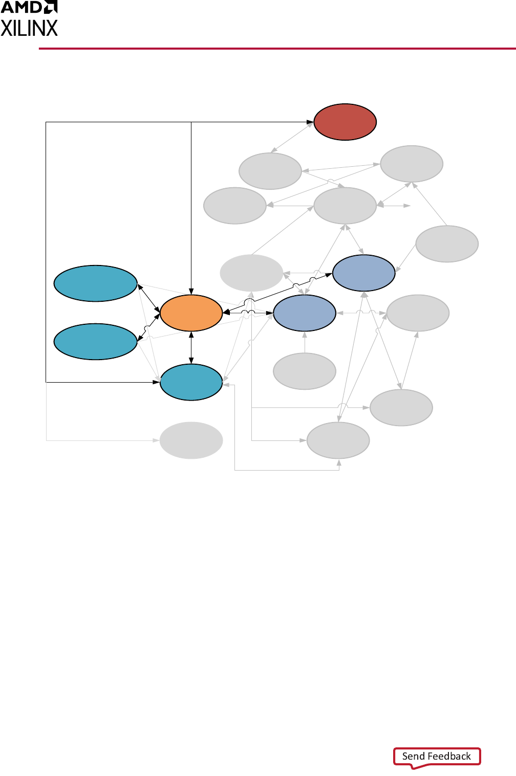
Vivado Properties Reference 114
UG912 (v2022.1) June 8, 2022 www.xilinx.com
Chapter2: Alphabetical List of First Class Objects
PACKAGE_PIN
Description
The PACKAGE_PIN object represents the physical pin on the Xilinx device package that is
associate with a specific input or output of the design. The assignment of I/O ports to a
package_pin is the subject of the Vivado Design Suite User Guide: I/O and Clock Planning
(UG899) [Ref 17].
The PACKAGE_PIN object can be assigned to PORT objects through the PACKAGE_PIN
property.
X-Ref Target - Figure 2-31
Figure2‐31 : PACKAGE_PIN Objects
Pin
Port
Clock
Cell
Bel
Site/CLB
Clock
Region
Package
Pin
Bel Pin
Site Pin
Site Pip
I/O
Standard
I/O Bank
Tile
Timing Path
SLR
PkgPin
_ByteGroup
PkgPin
_Nibble
X14875-081315

Vivado Properties Reference 115
UG912 (v2022.1) June 8, 2022 www.xilinx.com
Chapter2: Alphabetical List of First Class Objects
Related Objects
PACKAGE_PIN objects are associated with PORT objects in the design netlist, and with SITE,
BEL or IO_BANK objects on the target device. In addition, PACKAGE_PIN objects are
associated with PKGPIN_BYTEGROUP and PKGPIN_NIBBLE objects. The PACKAGE_PINs can
be queried through the use of the following Tcl command:
get_package_pins
Or, through associated objects with:
get_package_pins -of [get_ports]
You can also get the port, site, slr, io_bank, io_standard, pkgpin_bytegroup, phkgpin_nibble
associated with a specified package_pin:
get_port -of [get_package_pins AG17]
TIP: In this case, the ports can also be found by looking at the PACKAGE_PIN property:
get_ports -filter {PACKAGE_PIN==AG17}
Properties
The properties found on package_pin objects are as follows, with example values:
Property Type Read-only Visible Value
BANK string true true 44
BUFIO_2_REGION string true true BL
CLASS string true true package_pin
DIFF_PAIR_PIN string true true AE21
IS_BONDED bool true true 1
IS_DIFFERENTIAL bool true true 1
IS_GENERAL_PURPOSE bool true true 1
IS_GLOBAL_CLK bool true true 0
IS_LOW_CAP bool true true 0
IS_MASTER bool true true 1
IS_VREF bool true true 0
IS_VRN bool true true 0
IS_VRP bool true true 0
MAX_DELAY int true true 72405
MIN_DELAY int true true 71685
NAME string true true AD21
PIN_FUNC enum true true IO_L1P_T0L_N0_DBC_44
PIN_FUNC_COUNT int true true 1
The properties of package_pin objects can be listed with the following command:
report_property -all [lindex [get_package_pins] 0]

Vivado Properties Reference 116
UG912 (v2022.1) June 8, 2022 www.xilinx.com
Chapter2: Alphabetical List of First Class Objects
PIN
Description
A pin is a point of logical connectivity on a primitive or hierarchical cell. A pin allows the
contents of a cell to be abstracted away, and the logic simplified for ease-of-use. Pins can
be scalar, containing a single connection, or can be defined as bus pins to group multiple
signals together.
Related Objects
A pin is attached to a cell and can be connected to pins on other cells by a net. The pins of
cells are also related to the bel_pins of the bel object, or site_pins of a SITE that the cell is
mapped to. Pins are associated with clocks as part of the clock domain, and are part of
timing_paths when defined as the start point, end point, or through point of the path.
Pins can also be associated with drc_violations to allow you to more quickly locate and
resolve design issues.
X-Ref Target - Figure 2-32
Figure2‐32: PIN Objects
Net
Pin
Port
Clock
Cell
Bel
Site
Clock
Region
Package
Pin
Bel Pin
Site Pin
Site Pip
I/O
Standard
I/O Bank
Wire
Node
Pip
Tile
Timing
Path
X14876-081315

Vivado Properties Reference 117
UG912 (v2022.1) June 8, 2022 www.xilinx.com
Chapter2: Alphabetical List of First Class Objects
Properties
The PIN object includes a collection of properties that define the type of pin for clock and
control pins. You can use these attributes to filter the list of pins by type when writing Tcl
scripts, or working with PIN objects. The properties are listed in the table below.
Beyond these properties that define the pin type, the various properties found on PIN
objects include the following:
Property Type Read-only Visible Value
BEL string false true
BUS_DIRECTION enum true true
BUS_NAME string true true
BUS_START int true true
BUS_STOP int true true
BUS_WIDTH int true true
CLASS string true true pin
CLOCK_DEDICATED_ROUTE enum false true
DCI_VALUE int false true
DIRECTION enum true true IN
ESSENTIAL_CLASSIFICATION_VALUE int false true
FB_ACTIVE bool false true
HD.ASSIGNED_PPLOCS string* true true
HD.CLK_SRC string false true
HD.LOC_FIXED bool false false 0
HD.PARTPIN_LOCS string* false true
HD.PARTPIN_RANGE string* false true
HD.PARTPIN_TIEOFF bool false true
HD.TANDEM int false true
Table2‐2: Properties for PIN object
Property Name Clock Relationship Description Example
IS_CLEAR Asynchronous Forces block output(s) to a 0 state.
CLR pin in the
FDCE
IS_CLOCK Reference
The pin has a setup/hold or recovery/removal
relationship with another pin, and acts as the
reference pin in that relationship.
The C pin on an
FDRE
IS_ENABLE Synchronous
Control that allows or inhibits the data
capture of a block.
The CE pin on an
FDRE
IS_PRESET Asynchronous Forces block output(s) to a 1 state.
The PRE pin on
an FDPE
IS_RESET Synchronous
Changes block output(s) to a 0 state at next
clock.
The R pin on an
FDRE
IS_SET Synchronous
Changes block output(s) to a 1 state at next
clock.
The S pin on an
FDSE
IS_SETRESET Programmable
Programmable synchronous or asynchronous
set/reset. The pin's behavior is controlled by
an attribute on the block.
The RSTRAMB
pin on a
RAMB36E2
IS_WRITE_ENABLE Synchronous
Enable pin that allows or inhibits the write
operation on a memory block.
The WES pin on
a RAMB36E2

Vivado Properties Reference 118
UG912 (v2022.1) June 8, 2022 www.xilinx.com
Chapter2: Alphabetical List of First Class Objects
HIERARCHICALNAME string true false
top.cpuEngine.dwb_biu.\retry_cntr_reg[0] .C
HOLD_DETOUR int false true
HOLD_SLACK double true true needs timing update***
IS_CLEAR bool true true 0
IS_CLOCK bool true true 1
IS_CONNECTED bool true true 1
IS_ENABLE bool true true 0
IS_INVERTED bool false true 0
IS_LEAF bool true true 1
IS_ORIG_PIN bool true true 0
IS_PRESET bool true true 0
IS_RESET bool true true 0
IS_REUSED bool true true 0
IS_SET bool true true 0
IS_SETRESET bool true true 0
IS_WRITE_ENABLE bool true true 0
LOGIC_VALUE string true true unknown
MARK_DEBUG bool false true
NAME string true true
cpuEngine/dwb_biu/retry_cntr_reg[0]/C
ORIG_PIN_NAME string true true
PARENT_CELL cell true true
cpuEngine/dwb_biu/retry_cntr_reg[0]
REF_NAME string true true FDCE
REF_PIN_NAME string true true C
SETUP_SLACK double true true needs timing update***
TARGET_SITE_PINS string* false true
XLNX_LINE_COL int false false
XLNX_LINE_FILE long false false
The properties of pins can be listed with the following command:
report_property -all [lindex [get_pins] 0]

Vivado Properties Reference 119
UG912 (v2022.1) June 8, 2022 www.xilinx.com
Chapter2: Alphabetical List of First Class Objects
PIP or SITE_PIP
Description
A PIP is a device object used for routing connections, or NETs, on the Xilinx part. A PIP, also
called an ARC, is a connection multiplexer that can be programmed to connect one WIRE to
another, thus connecting NODEs together to form the routing required for a specific NET in
the design.
A SITE_PIP, also known as a routing BEL, is a connection multiplexer inside a SITE that can
connect BEL_PINs to other BEL_PINs, or to SITE_PINs within the SITE.
X-Ref Target - Figure 2-33
Figure2‐33 : PIP Objects
Net
Pin
Port
Clock
Cell
Bel
Site/CLB
Clock
Region
Package
Pin
Bel Pin
Site Pin
Site Pip
I/O
Standard
I/O Bank
Wire
Node
Pip
Tile
Timing
Path
SLR
PkgPin
_ByteGroup
PkgPin
_Nibble
X14877-081315

Vivado Properties Reference 120
UG912 (v2022.1) June 8, 2022 www.xilinx.com
Chapter2: Alphabetical List of First Class Objects
Related Objects
As seen in Figure 2-33, page 119, PIP objects are related to SLRs, TILEs, NODEs, NETs, and
WIREs. You can query the PIPs using a form of the following Tcl command:
get_pips -of [get_nodes INT_R_X7Y47/NW6BEG1]
You can also query the SLRs, and TILEs that PIPs are located in; or the NODEs,
SPEED_MODELs, or WIREs associated with specific PIPs:
get_nodes -of_objects [get_pips INT_R_X7Y47/INT_R.BYP_ALT0->>BYP_BOUNCE0]
SITE_PIPs are associated with SITEs:
get_site_pips -of [get_sites SLICE_X8Y79]
PIP Properties
The properties on a PIP object can be reported with a command such as the following:
report_property -all [lindex [get_pips -of [get_tiles INT_R_X7Y47]] 0]
TIP: Due to the number of PIPs on a device, using the get_pips Tcl command without -of_objects
or -filters to narrow the results is not recommended.
The properties include the following, with example values:
Property Type Read-only Visible Value
CAN_INVERT bool true true 0
CLASS string true true pip
IS_BUFFERED_2_0 bool true true 0
IS_BUFFERED_2_1 bool true true 1
IS_DIRECTIONAL bool true true 1
IS_EXCLUDED_PIP bool true true 0
IS_FIXED_INVERSION bool true true 0
IS_INVERTED bool true true 0
IS_PSEUDO bool true true 0
IS_SITE_PIP bool true true 0
IS_TEST_PIP bool true true 0
NAME string true true INT_R_X7Y47/INT_R.BYP_ALT0->>BYP_BOUNCE0
SPEED_INDEX int true true 2336
TILE string true true INT_R_X7Y47
VORPAL_ID int true false

Vivado Properties Reference 121
UG912 (v2022.1) June 8, 2022 www.xilinx.com
Chapter2: Alphabetical List of First Class Objects
SITE_PIP Properties
The properties of the SITE_PIP can be reported with the following command:
get_site_pips -of [get_sites SLICE_X8Y79]
The properties on the SITE_PIP include the following, with example values:
Property Type Read-only Visible Value
CLASS string true true site_pip
FROM_PIN string true true A1
IS_FIXED bool true true 0
IS_USED bool true true 0
NAME string true true SLICE_X8Y79/D6LUT:A1
SITE string true true SLICE_X8Y79
TO_PIN string true true O6

Vivado Properties Reference 122
UG912 (v2022.1) June 8, 2022 www.xilinx.com
Chapter2: Alphabetical List of First Class Objects
PKGPIN_BYTEGROUP
Description
For 7 series devices, the hierarchy of I/O banks is divided into two object types: I/O Banks
and Package Pins. For Xilinx UltraScale architecture, the I/O bank hierarchy includes two
additional divisions: bytegroups and nibbles. The relationships of these objects on an
UltraScale device are defined as follows:
•An IO_BANK of 52 pins has 4 pkgpin_bytegroups, while a mini IO_BANK of 26 pins has 2
bytegroups.
• Each pkgpin_bytegroup has 13 package pins, and has 2 pkgpin_nibbles, an upper and
lower.
X-Ref Target - Figure 2-34
Figure2‐34: PKGPIN_BYTEGROUP Objects
Pin
Port
Clock
Cell
Bel
Site/CLB
Clock
Region
Package
Pin
Bel Pin
Site Pin
Site Pip
I/O
Standard
I/O Bank
Tile
Timing Path
SLR
PkgPin
_ByteGroup
PkgPin
_Nibble
X14878-081315

Vivado Properties Reference 123
UG912 (v2022.1) June 8, 2022 www.xilinx.com
Chapter2: Alphabetical List of First Class Objects
• Each pkgpin_nibble has 6 or 7 pins, and is the upper or lower nibble of the
pkgpin_bytegroup.
• A package_pin is one pin of an iobank, a pkgpin_bytegroup, or a pkgpin_nibble.
In UltraScale, the bitslice logic connected to I/O banks is grouped into pkgpin_bytegroups
and pkgpin_nibbles. These objects aid in the placement of related I/O pins, such as groups
of bitslices. For instance, you can use bytegroups and nibbles for I/O pin assignment of
memory controllers on UltraScale devices. You can perform interactive I/O planning by
opening either the elaborated RTL design or the synthesized design in the Vivado IDE, using
the Memory Bank/Byte Planner, which enables automatic or manual assignment of memory
I/O pin groups to I/O banks and byte lanes. This process is discussed in detail at this link in
the Vivado Design Suite User Guide: I/O and Clock Planning (UG899) [Ref 17].
Related Objects
The PKGPIN_BYTEGROUP and PKGPIN_NIBBLE are related to IO_BANKs, PACKAGE_PINs, and
PORTs, as previously described. In addition, each PKGPIN_BYTEGROUP is related to a SITE
on the Xilinx device. You can query the PKGPIN_BYTEGROUP of an associated object using
a Tcl command like the following:
get_pkgpin_bytegroups -of [get_package_pins AG17]
You can also get the list of package_pin objects assigned to specific pkgpin_bytegroups:
get_package_pins -of [get_pkgpin_bytegroups BANK45_BYTE2]
Properties
The properties found on PKGPIN_BYTEGROUP objects are as follows, with example values:
Property Type Read-only Value
CLASS string true pkgpin_bytegroup
INDEX_IN_IOBANK int true 2
IOBANK int true 45
NAME string true BANK45_BYTE2
The properties of the bytegroup objects can be listed with the following command:
report_property -all [lindex [get_pkgpin_bytegroups] 0]
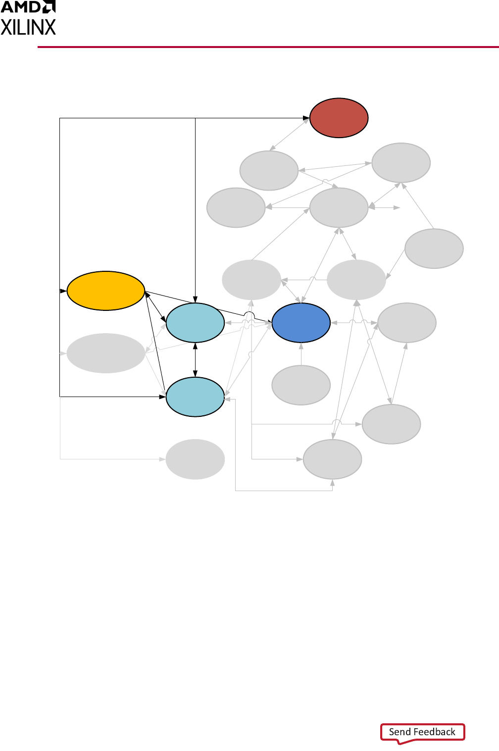
Vivado Properties Reference 124
UG912 (v2022.1) June 8, 2022 www.xilinx.com
Chapter2: Alphabetical List of First Class Objects
PKGPIN_NIBBLE
Description
The PKGPIN_NIBBLE is a portion of the PKGPIN_BYTEGROUP. Refer to PKGPIN_BYTEGROUP,
page 122 for a description of this object.
Related Objects
The PKGPIN_BYTEGROUP and PKGPIN_NIBBLE are related to IO_BANKs, PACKAGE_PINs, and
PORTs, as previously described. In addition, each PKGPIN_NIBBLE is related to a SITE on the
Xilinx device. You can query the PKGPIN_NIBBLE of an associated object using a Tcl
command like the following:
X-Ref Target - Figure 2-35
Figure2‐35: PKGPIN_NIBBLE Objects
Pin
Port
Clock
Cell
Bel
Site/CLB
Clock
Region
Package
Pin
Bel Pin
Site Pin
Site Pip
I/O
Standard
I/O Bank
Tile
Timing Path
SLR
PkgPin
_ByteGroup
PkgPin
_Nibble
X14880-081315

Vivado Properties Reference 125
UG912 (v2022.1) June 8, 2022 www.xilinx.com
Chapter2: Alphabetical List of First Class Objects
get_pkgpin_nibbles -of [get_iobanks 45]
You can also get the list of package_pin objects assigned to specific pkgpin_nibbles:
get_package_pins -of [get_pkgpin_nibbles BANK45_BYTE2_L]
Properties
The properties found on pkgpin_nibble objects are as follows, with example values:
Property Type Read-only Value
CLASS string true pkgpin_nibble
IOBANK int true 45
NAME string true BANK45_BYTE2_L
PKGPIN_BYTEGROUP string true BANK45_BYTE2
TYPE string true L
The properties of pkgpin_nibble objects can be listed with the following command:
report_property -all [lindex [get_pkgpin_nibbles] 0]

Vivado Properties Reference 126
UG912 (v2022.1) June 8, 2022 www.xilinx.com
Chapter2: Alphabetical List of First Class Objects
PORT
Description
A port is a special type of hierarchical pin, providing an external connection point at the
top-level of a hierarchical design, or an internal connection point in a hierarchical cell or
block module to connect the internal logic to the pins on the hierarchical cell. Ports can be
scalar, containing a single connection, or can be bus ports to group multiple signals
together.
X-Ref Target - Figure 2-36
Figure2‐36: PORT Objects
Net
Pin
Port
Clock
Cell
Bel
Site/CLB
Clock
Region
Package
Pin
Site Pin
Site Pip
I/O
Standard
I/O Bank
Wire
Node
Pip
Tile
Timing
Path
SLR
PkgPin
_ByteGroup
PkgPin
_Nibble
Bel Pin
X14881-081315

Vivado Properties Reference 127
UG912 (v2022.1) June 8, 2022 www.xilinx.com
Chapter2: Alphabetical List of First Class Objects
Related Objects
Ports at the top level of the design make connection outside the FPGA through the
PACKAGE_PINs of the device package, to IO_BANKs on the die, with assigned
IOSTANDARDs.
Ports can also carry clock definitions onto the design from the system or board, and should
be assigned external system-level path delay using the set_input_delay or
set_output_delay constraints. Refer to the Vivado Design Suite User Guide: Using
Constraints (UG903) [Ref 19] for more information on these constraints.
You can query the ports assigned to specific package_pins, IO_banks, IO_Standards, sites,
cells, nets, clocks, timing_paths, or drc_violations using a Tcl command like the following:
get_ports -of [get_clocks]
Inside the design, ports are connected to cells, through nets, to build the hierarchical
netlist. You can query the objects associated with a port, such as net, timing_path, site,
io_bank, io_standard, package_pin, pkgpin_bytegroup, pkgpin_nibble, using the following
form of command:
get_package_pins -of [all_inputs]
Properties
The properties found on ports objects are as follows, with example values:
Property Type Read-only Visible Value
BOARD_PART_PIN string false true
BOARD_PIN string false false
BUFFER_TYPE enum false true
BUS_DIRECTION enum true true
BUS_NAME string true true
BUS_START int true true
BUS_STOP int true true
BUS_WIDTH int true true
CLASS string true true port
CLOCK_BUFFER_TYPE enum false true
DIFFTERMTYPE bool false false 0
DIFF_PAIR_PORT string true true
DIFF_PAIR_TYPE enum true true
DIFF_TERM bool false true 0
DIRECTION enum false true IN
DQS_BIAS enum false true
DRIVE enum false true 12
DRIVE_STRENGTH enum false false 12
ESSENTIAL_CLASSIFICATION_VALUE int false true
HD.ASSIGNED_PPLOCS string* true true
HD.CLK_SRC string false true
HD.LOC_FIXED bool false false 0
HD.PARTPIN_LOCS string* false true
HD.PARTPIN_RANGE string* false true
HD.PARTPIN_TIEOFF bool false true

Vivado Properties Reference 128
UG912 (v2022.1) June 8, 2022 www.xilinx.com
Chapter2: Alphabetical List of First Class Objects
HOLD_SLACK double true true needs timing update***
IBUF_LOW_PWR bool false true 0
INTERFACE string false true
INTERMTYPE enum false false NONE
IN_TERM enum false true NONE
IOB enum false true
IOBANK int true true 33
IOSTANDARD enum false true LVCMOS18
IOSTD enum false false LVCMOS18
IO_BUFFER_TYPE enum false true
IS_BEL_FIXED bool false false 1
IS_FIXED bool false false 1
IS_GT_TERM bool true true 0
IS_LOC_FIXED bool false true 1
IS_REUSED bool true true
KEEP string false true
KEEPER bool false false 0
LOAD double false true
LOC site false true IOB_X1Y43
LOGIC_VALUE string true true unknown
NAME string false true reset
OFFCHIP_TERM string false true NONE
OUT_TERM enum false true
PACKAGE_PIN package_pin false true W9
PIN_TYPE enum true false
PIO_DIRECTION enum false true
PULLDOWN bool false false 0
PULLTYPE string false true
PULLUP bool false false 0
SETUP_SLACK double true true needs timing update***
SITE site false false IOB_X1Y43
SLEW enum false true
SLEWTYPE enum false false
SLEW_ADV enum false false
UNCONNECTED bool true true 0
USE_INTERNAL_VREF enum false true
VCCAUX_IO enum false true
XLNX_LINE_COL int false false
XLNX_LINE_FILE long false false
X_INTERFACE_INFO string false true
The properties of ports can be listed with the following command:
report_property -all [lindex [get_ports] 0]

Vivado Properties Reference 129
UG912 (v2022.1) June 8, 2022 www.xilinx.com
Chapter2: Alphabetical List of First Class Objects
SITE
Description
A SITE is a device object representing one of many different types of logic resources
available on the target Xilinx FPGA.
SITEs include SLICE/CLBs which are collections of basic logic elements (BELs) like
look-up-tables (LUTs), flip-flops, muxes, carry logic resources to implement fast addition,
subtraction, or comparison operations. SLICE/CLBs have wide multiplexers, and dedicated
carry chains running vertically from SLICE to SLICE.
X-Ref Target - Figure 2-37
Figure2‐37: SITE Objects
Net
Pin
Port
Clock
Cell
Bel
Site/CLB
Clock
Region
Package
Pin
Site Pin
Site Pip
I/O
Standard
I/O Bank
Wire
Node
Pip
Tile
Timing
Path
SLR
PkgPin
_ByteGroup
PkgPin
_Nibble
Bel Pin
X14882-081315

Vivado Properties Reference 130
UG912 (v2022.1) June 8, 2022 www.xilinx.com
Chapter2: Alphabetical List of First Class Objects
There are two types of SLICEs in a device:
• SLICEMs can be configured to act as distributed RAM. Distributed Memory is a
configuration feature of certain LUTs so it behaves as a small 64-bit memory.
• SLICEL LUTs can only function as logic and not memory.
Two SLICEs are grouped together into a configurable logic block (CLB) in 7 series FPGAs.
Two CLBs are grouped together into one TILE object on the device. Each UltraScale
architecture CLB contains one SLICE. See the 7 Series FPGAs Configurable Logic Block User
Guide (UG474) [Ref 4] or UltraScale Architecture Configurable Logic Block User Guide
(UG574) [Ref 10] for more information.
SITEs also contain varied device resources such as block RAM, DSPs, I/O blocks, Clock
resources, and GT blocks.
You utilize device resources by inference from the HDL source by Vivado synthesis, or by
instantiating a primitive or macro from the FPGA library, or an IP core from the Vivado IP
catalog. The Vivado Design Suite 7 Series FPGA and Zynq-7000 SoC Libraries Guide (UG953)
[Ref 25] and UltraScale Architecture Libraries Guide (UG974) [Ref 26] describe the list of
primitives that can be instantiated.
The available SITE types vary depending on the Xilinx device in use. Some of the SITE types
include:
AMS_ADC AMS_DAC
BSCAN BSCAN_JTAG_MONE2
BUFG BUFGCTRL BUFG_LB BUFHCE
BUFIO BUFMRCE BUFR
CAPTURE
DCIRESET DNA_PORT
DRP_AMS_ADC DRP_AMS_DAC
DSP48E1
EFUSE_USR
FIFO18E1 FIFO36E1
FRAME_ECC
GLOBALSIG
GTHE2_CHANNEL GTHE2_COMMON
GTPE2_CHANNEL GTPE2_COMMON
GTXE2_CHANNEL GTXE2_COMMON
GTZE2_OCTAL
IBUFDS_GTE2 ICAP
IDELAYCTRL IDELAYE2 IDELAYE2_FINEDELAY
ILOGICE2 ILOGICE3
IN_FIFO
IOB IOB18 IOB18M IOB18S
IOB33 IOB33M IOB33S
IOBM IOBS
IPAD ISERDESE2
KEY_CLEAR
MMCME2_ADV
ODELAYE2 ODELAYE2_FINEDELAY
OLOGICE2 OLOGICE3
OPAD

Vivado Properties Reference 131
UG912 (v2022.1) June 8, 2022 www.xilinx.com
Chapter2: Alphabetical List of First Class Objects
OSERDESE2
OUT_FIFO
PCIE_2_1 PCIE_3_0
PHASER_IN PHASER_IN_ADV PHASER_IN_PHY
PHASER_OUT PHASER_OUT_ADV PHASER_OUT_PHY
PHASER_REF
PHY_CONTROL
PLLE2_ADV PMV2
RAMB18E1 RAMB36E1 RAMBFIFO36E1
SLICEL SLICEM
STARTUP TIEOFF
USR_ACCESS
XADC
Related Objects
As seen in Figure 2-37, page 129, SITEs are related to many different netlist and device
objects. Leaf-CELLs like flops and latches are mapped to BELs which are in turn mapped to
SITEs like SLICEL and SLICEM, or are mapped directly to SITEs such as BRAMs and DSPs. BELs
and SITEs are grouped into TILEs, and are assigned to CLOCK_REGIONs and SLRs on the
device. PORTs, PINs, IO_BANKs, and PACKAGE_PINs relate to IO blocks (IOBs) which are also
SITEs. SITEs also have pins, or SITE_PINs, that map to NODEs, PIPs, PINs, and NETs. You can
query the sites associated with any of these objects as follows:
get_sites -of [get_cells -hier microblaze_0]
You can also use the SITE to query associated objects such as CELL, PORT, BEL, BEL_PIN,
CLOCK_REGION, SITE_PIN, SLR, TILE, IO_BANK, IO_STANDARD, PACKAGE_PIN,
PKGPIN_BYTEGROUP, PKGPIN_NIBBLE, PIP, and SITE_PIP. For example:
get_clock_regions -of [get_sites DSP48E2_X2Y119]
Properties
There are over 80 different SITE types on Xilinx FPGA devices, but they all share the
following properties, with example values provided:
Property Type Read-only Visible Value
ALTERNATE_SITE_TYPES string true true IOB33S IOB33M
CLASS string true true site
CLOCK_REGION string true true X0Y6
IS_BONDED bool true true 1
IS_CLOCK_BUFFER bool true true 0
IS_CLOCK_PAD bool true true 0
IS_GLOBAL_CLOCK_BUFFER bool true true 0
IS_GLOBAL_CLOCK_PAD bool true true 0
IS_PAD bool true true 1
IS_REGIONAL_CLOCK_BUFFER bool true true 0
IS_REGIONAL_CLOCK_PAD bool true true 0
IS_RESERVED bool true true 0
IS_TEST bool true true 0
IS_USED bool true true 0
MANUAL_ROUTING string false true

Vivado Properties Reference 132
UG912 (v2022.1) June 8, 2022 www.xilinx.com
Chapter2: Alphabetical List of First Class Objects
NAME string true true IOB_X0Y349
NUM_ARCS int true true 9
NUM_BELS int true true 7
NUM_INPUTS int true true 12
NUM_OUTPUTS int true true 5
NUM_PINS int true true 17
PRIMITIVE_COUNT int true true 0
PROHIBIT bool false true 0
PROHIBIT_FROM_PERSIST bool true true 0
RPM_X int true true 1
RPM_Y int true true 698
SITE_PIPS string false true
SITE_TYPE enum true true IOB33
The properties assigned to SITE objects are the same for all SITE_TYPEs. To report the
properties for any of the SITE_TYPEs listed above, you can use the report_property
command:
report_property -all [lindex [get_sites -filter {SITE_TYPE == <SITE_TYPE>}] 0]
Where <SITE_TYPE> should be replaced by one of the listed SITE types. For example:
report_property -all [lindex [get_sites -filter {SITE_TYPE == DSP48E1}] 0]
report_property -all [lindex [get_sites -filter {SITE_TYPE == RAMB36E1}] 0]
report_property -all [lindex [get_sites -filter {SITE_TYPE == IBUFDS_GTE2}] 0]

Vivado Properties Reference 133
UG912 (v2022.1) June 8, 2022 www.xilinx.com
Chapter2: Alphabetical List of First Class Objects
SLR
Description
A Super Logic Region (SLR) is a single FPGA die slice contained in an stacked silicon
interconnect (SSI) device. Stacked silicon interconnect (SSI) technology uses passive silicon
interposers with microbumps and through-silicon vias (TSVs) to combine multiple FPGA die
slices, referred to as super logic regions (SLRs), into a single package.
Each SLR contains the active circuitry common to most Xilinx FPGA devices, and are
connected through super long lines (SLLs) found on the silicon interposers. Refer to this link
in the UltraFast Design Methodology Guide for the Vivado Design Suite (UG949) [Ref 24] for
more information on working with SSI components.
X-Ref Target - Figure 2-38
Figure2‐38: SLR Objects
Net
Pin
Port
Clock
Cell
Bel
Site/CLB
Clock
Region
Package
Pin
Bel Pin
Site Pin
I/O
Standard
I/O Bank
Wire
Node
Pip
Tile
Timing
Path
SLR
Site Pip
X14884-081315

Vivado Properties Reference 134
UG912 (v2022.1) June 8, 2022 www.xilinx.com
Chapter2: Alphabetical List of First Class Objects
Related Objects
Super logic regions (SLRs) are die slices of Xilinx FPGA architecture or devices. As shown in
Figure 2-38, page 133, each SLR contains clock regions, tiles, sites, site pins, bels, bel pins,
nodes, pips, cells, pins, I/O banks, and package pins. You can find the SLRs associated with
each of these different types of objects, with a Tcl command such as the following, that
returns the SLR that the specified cell is assigned to:
get_slrs -of [get_cells DataIn_pad_0_i_IBUF[3]_inst]
You can also query the clock regions, tiles, sites, or bels associated with an SLR. The
following Tcl command gets I/O banks of the clock regions associated with a specific SLR:
get_iobanks -of [get_clock_regions -of [get_slrs SLR3]]
Properties
You can use the report_property command to report the properties of an SLR. Refer to
the Vivado Design Suite Tcl Command Reference Guide (UG835) [Ref 13] for more
information. The properties on the SLR object include the following, with example values:
Property Type Read-only Visible Value
ARCH string true true virtex7
CHIP_TYPE string true true xc7vx1140t 0
CLASS string true true slr
CONFIG_ORDER_INDEX int true true 0
IS_FABRIC bool true true 1
IS_MASTER bool true true 1
LOWER_RIGHT_CORNER int true true (0,157)
LOWER_RIGHT_X int true true 0
LOWER_RIGHT_Y int true true 157
MAX_SITE_INDEX int true true 278381
MAX_TILE_INDEX int true true 266114
MIN_SITE_INDEX int true true 185588
MIN_TILE_INDEX int true true 177410
NAME string true true SLR1
NUM_CHANNELS int true true 220
NUM_SITES int true true 92794
NUM_SLLS int true true 10780
NUM_TILES int true true 23169
NUM_TOP_CLOCK_CONNECTIONS int true true 32
NUM_TOP_DATA_CONNECTIONS int true true 10780
SLR_INDEX int true true 1
UPPER_LEFT_CORNER int true true (564,313)
UPPER_LEFT_X int true true 564
UPPER_LEFT_Y int true true 313
To report the properties for a specific SLR, you can copy and paste the following command
into the Vivado Design Suite Tcl shell or Tcl Console:
report_property -all [get_slrs <name>]
Where <name> is the name of the SLR to report.

Vivado Properties Reference 135
UG912 (v2022.1) June 8, 2022 www.xilinx.com
Chapter2: Alphabetical List of First Class Objects
TILE
Description
A TILE is a device object containing one or more SITE objects. Programmable logic TILEs
include diverse objects such as SLICE/CLBs, BRAM, DSPs, I/O Blocks, Clock resources, and
GT blocks. Structurally, each tile has a number of inputs and outputs and the programmable
interconnect to connect the inputs and outputs of a tile to any other tile.
There are many different types of TILEs, depending on the Xilinx device in use. Available
TILE_TYPEs include the following:
AMS_ADC_TOP AMS_BRAM
AMS_CLB_INTF_IOB AMS_CLK AMS_CMT
AMS_DAC_TOP AMS_DRP_ADC_TOP AMS_DRP_DAC_TOP
X-Ref Target - Figure 2-39
Figure2‐39 : TILE Objects
Net
Pin
Port
Clock
Cell
Bel
Site
Clock
Region
Package
Pin
Bel Pin
Site Pin
Site Pip
I/O
Standard
I/O Bank
Wire
Node
Pip
Tile
Timing
Path
SLR
X14885-081315

Vivado Properties Reference 136
UG912 (v2022.1) June 8, 2022 www.xilinx.com
Chapter2: Alphabetical List of First Class Objects
AMS_DSP AMS_INT AMS_INT_L AMS_INT_R
AMS_IOI AMS_VBRK_INTF
BRAM_INT_INTERFACE_L BRAM_INT_INTERFACE_R
BRAM_L BRAM_R
BRKH_BRAM BRKH_B_TERM_INT
BRKH_CLB BRKH_CLK BRKH_CMT
BRKH_DSP_L BRKH_DSP_R BRKH_GTX
BRKH_INT BRKH_TERM_INT B_TERM_INT B_TERM_INT_SLV
CFG_CENTER_BOT CFG_CENTER_MID CFG_CENTER_MID_SLAVE
CFG_CENTER_TOP CFG_CENTER_TOP_SLAVE
CLBLL_L CLBLL_R CLBLM_L CLBLM_R
CLK_BALI_REBUF CLK_BALI_REBUF_GTZ_BOT CLK_BALI_REBUF_GTZ_TOP
CLK_BUFG_BOT_R CLK_BUFG_REBUF CLK_BUFG_TOP_R
CLK_FEED
CLK_HROW_BOT_R CLK_HROW_TOP_R
CLK_MTBF2
CLK_PMV CLK_PMV2 CLK_PMV2_SVT CLK_PMVIOB
CLK_TERM
CMT_FIFO_L CMT_FIFO_R
CMT_PMV CMT_PMV_L
CMT_TOP_L_LOWER_B CMT_TOP_L_LOWER_T
CMT_TOP_L_UPPER_B CMT_TOP_L_UPPER_T
CMT_TOP_R_LOWER_B CMT_TOP_R_LOWER_T
CMT_TOP_R_UPPER_B CMT_TOP_R_UPPER_T
DSP_L DSP_R
GTH_CHANNEL_0 GTH_CHANNEL_1 GTH_CHANNEL_2 GTH_CHANNEL_3 GTH_COMMON
GTH_INT_INTERFACE GTH_INT_INTERFACE_L
GTX_CHANNEL_0 GTX_CHANNEL_1 GTX_CHANNEL_2 GTX_CHANNEL_3 GTX_COMMON
GTX_INT_INTERFACE GTX_INT_INTERFACE_L
GTZ_BOT GTZ_BRAM
GTZ_CLB_INTF_IOB GTZ_CLK GTZ_CLK_B GTZ_CMT
GTZ_DSP
GTZ_INT GTZ_INT_L GTZ_INT_LB GTZ_INT_R GTZ_INT_RB
GTZ_IOI GTZ_TOP GTZ_VBRK_INTF
HCLK_BRAM HCLK_CLB
HCLK_CMT HCLK_CMT_L
HCLK_DSP_L HCLK_DSP_R
HCLK_FEEDTHRU_1 HCLK_FEEDTHRU_2
HCLK_FIFO_L
HCLK_GTX
HCLK_INT_INTERFACE HCLK_IOB
HCLK_IOI HCLK_IOI3
HCLK_L HCLK_L_BOT_UTURN HCLK_L_SLV HCLK_L_TOP_UTURN
HCLK_R HCLK_R_BOT_UTURN HCLK_R_SLV HCLK_R_TOP_UTURN
HCLK_TERM HCLK_TERM_GTX HCLK_VBRK HCLK_VFRAME
INT_FEEDTHRU_1 INT_FEEDTHRU_2
INT_INTERFACE_L INT_INTERFACE_R
INT_L INT_L_SLV INT_L_SLV_FLY
INT_R INT_R_SLV INT_R_SLV_FLY
IO_INT_INTERFACE_L IO_INT_INTERFACE_R
LIOB18 LIOB18_SING LIOB33 LIOB33_SING
LIOI LIOI3 LIOI3_SING LIOI3_TBYTESRC LIOI3_TBYTETERM
LIOI_SING LIOI_TBYTESRC LIOI_TBYTETERM
L_TERM_INT L_TERM_INT_BRAM
MONITOR_BOT MONITOR_BOT_SLAVE MONITOR_MID MONITOR_TOP
NULL
PCIE3_BOT_RIGHT PCIE3_INT_INTERFACE_L PCIE3_INT_INTERFACE_R
PCIE3_RIGHT PCIE3_TOP_RIGHT PCIE_BOT
PCIE_BOT_LEFT PCIE_INT_INTERFACE_L PCIE_INT_INTERFACE_LEFT_L

Vivado Properties Reference 137
UG912 (v2022.1) June 8, 2022 www.xilinx.com
Chapter2: Alphabetical List of First Class Objects
PCIE_INT_INTERFACE_R
PCIE_NULL PCIE_TOP PCIE_TOP_LEFT
RIOB18 RIOB18_SING RIOI RIOI_SING
RIOI_TBYTESRC RIOI_TBYTETERM
R_TERM_INT R_TERM_INT_GTX
TERM_CMT
T_TERM_INT T_TERM_INT_SLV
VBRK VBRK_EXT
VFRAME
Related Objects
TILE objects are associated with SLR, CLOCK_REGION, SITE, SITE_PIN, BEL and BEL_PIN
device resources, with NODE, WIRE, and PIP routing resources, and with the NET netlist
object.
For example, you can query the TILE of a related object using the following command,
which returns the tiles the specified net travels through:
get_tiles -of_objects [get_nets wbClk]
In addition, you can query the SLR, CLOCK_REGION, NODE, PIP, WIRE, SITE, BEL, and NET
objects associated with or found in a TILE.
get_bels -of_objects [get_tiles -filter {TILE_TYPE == GTX_CHANNEL_1}]
Properties
Although there are many different types of TILE objects, as represented by the TILE_TYPE
property, all TILE objects have the same set of properties.
You can use the report_property command to report the properties of a TILE object.
Refer to the Vivado Design Suite Tcl Command Reference Guide (UG835) [Ref 13] for more
information.
The properties on a CLBLL type of TILE object include the following, with example values:
Property Type Read-only Visible Value
CLASS string true true tile
COLUMN int true true 50
DEVICE_ID int true true 0
FIRST_SITE_ID int true true 46
GRID_POINT_X int true true 50
GRID_POINT_Y int true true 1
INDEX int true true 167
INT_TILE_X int true true 17
INT_TILE_Y int true true 0
IS_CENTER_TILE bool true true 1
IS_DCM_TILE bool true true 0
IS_GT_CLOCK_SITE_TILE bool true true 0
IS_GT_SITE_TILE bool true true 0
NAME string true true CLBLL_L_X18Y199
NUM_ARCS int true true 146

Vivado Properties Reference 138
UG912 (v2022.1) June 8, 2022 www.xilinx.com
Chapter2: Alphabetical List of First Class Objects
NUM_SITES int true true 2
ROW int true true 1
SLR_REGION_ID int true true 0
TILE_PATTERN_IDX int true true 13
TILE_TYPE enum true true CLBLL_L
TILE_TYPE_INDEX int true true 19
TILE_X int true true -16260
TILE_Y int true true 320944
TYPE string true true CLBLL_L
To report the properties for any of the TILE_TYPEs listed previously, you can use the
following form of the report_property command:
report_property -all [lindex [get_sites -filter {TILE_TYPE == <TILE_TYPE>}] 0]
Where <SITE_TYPE> should be replaced by one of the listed SITE types. For example:
report_property -all [lindex [get_tiles -filter {TILE_TYPE == DSP_L}] 0]
report_property -all [lindex [get_tiles -filter {TILE_TYPE == BRAM_L}] 0]
report_property -all [lindex [get_tiles -filter {TILE_TYPE == GTX_CHANNEL_1}] 0]

Vivado Properties Reference 139
UG912 (v2022.1) June 8, 2022 www.xilinx.com
Chapter2: Alphabetical List of First Class Objects
TIMING_PATH
Description
Timing paths are defined by connections between elements of the design. In digital
designs, timing paths are formed by a pair of sequential elements controlled by the same
clock, or by two different clocks to launch and capture the signal.
In a typical timing path, the data is transferred between two sequential cells within one
clock period. For example, the launch edge occurs at time 0 ns; and the capture edge occurs
one CLOCK period later.
The most common timing paths are:
• Paths from an input port to a internal sequential cell
• Internal paths from one sequential cell to another sequential cell
• Paths from an internal sequential cell to an output port
• Paths from an input port to an output port
Each timing path is defined by unique startpoints, throughpoints, and endpoints. A path
startpoint is a sequential cell clock pin or a data input port; and a path endpoint is a
sequential cell data input pin or a data output port.
TIMING_PATH objects can be selected or specified with varying degrees of details. A single
unique timing path is defined by a combination of startpoint, throughpoint, and endpoint.
Multiple timing paths can be specified from a common startpoint, or a common endpoint.
Constraints can be applied to timing paths as determined by the definition of the timing
path. The order of precedence for constraints applied to timing paths, from highest to
lowest, is as follows:
1. -from -through -to (a unique timing path)
2. -from -to
3. -from -through
4. -from
5. -through -to
6. -to
7. -through (any timing path passing through this point)
For more information on timing paths refer to Vivado Design Suite User Guide: Design
Analysis and Closure Techniques (UG906) [Ref 22].

Vivado Properties Reference 140
UG912 (v2022.1) June 8, 2022 www.xilinx.com
Chapter2: Alphabetical List of First Class Objects
Related Objects
TIMING_PATH objects can be queried using the get_timing_paths command. This allows
you to specify timing paths using related CLOCK, PIN, PORT, or CELL objects to identify
startpoints, throughpoints, or endpoints on the paths of interest.
get_timing_paths -from fftEngine/control_reg_reg[1] -max_paths 10
In addition, you can query the CELL, NET, PIN, or PORT objects associated with specified
timing paths:
get_nets -of_objects [get_timing_paths -max_paths 10]
Properties
The properties on a TIMING_PATH object include the following, with example values:
Property Type Read-only Visible Value
CLASS string true true timing_path
CLOCK_PESSIMISM double true true -0.661
CORNER string true true Slow
DATAPATH_DELAY double true true 6.934
DELAY_TYPE string true true max
X-Ref Target - Figure 2-40
Figure2‐40: TIMING_PATH Objects
Net
Pin
Port
Clock
Cell
Bel
Site/CLB
Clock
Region
Package
Pin
Site Pin
Site Pip
I/O
Standard
I/O Bank
Wire
Node
Pip
Tile
Timing
Path
SLR
PkgPin
_ByteGroup
PkgPin
_Nibble
Bel Pin
X14886-081315

Vivado Properties Reference 141
UG912 (v2022.1) June 8, 2022 www.xilinx.com
Chapter2: Alphabetical List of First Class Objects
ENDPOINT_CLOCK clock true true cpuClk_3
ENDPOINT_CLOCK_DELAY double true true -2.149
ENDPOINT_CLOCK_EDGE double true true 20.000
ENDPOINT_PIN pin true true
cpuEngine/or1200_immu_top/qmemimmu_cycstb_o_reg/D
EXCEPTION string true true
GROUP string true true cpuClk_3
INPUT_DELAY double true true
INTER_SLR_COMPENSATION double true true
LOGIC_LEVELS int true true 16
NAME string true true {usbEngine0/u4/inta_reg/C -->
cpuEngine/or1200_immu_top/qmemimmu_cycstb_o_reg/D}
OUTPUT_DELAY double true true
REQUIREMENT double true true 10.000
SKEW double true true -0.057
SLACK double true true 2.865
STARTPOINT_CLOCK clock true true usbClk_2
STARTPOINT_CLOCK_DELAY double true true -2.754
STARTPOINT_CLOCK_EDGE double true true 10.000
STARTPOINT_PIN pin true true usbEngine0/u4/inta_reg/C
UNCERTAINTY double true true 0.202
USER_UNCERTAINTY double true true
The properties of TIMING_PATH objects can be reported with the following command:
report_property -all [lindex [get_timing_paths] 0]
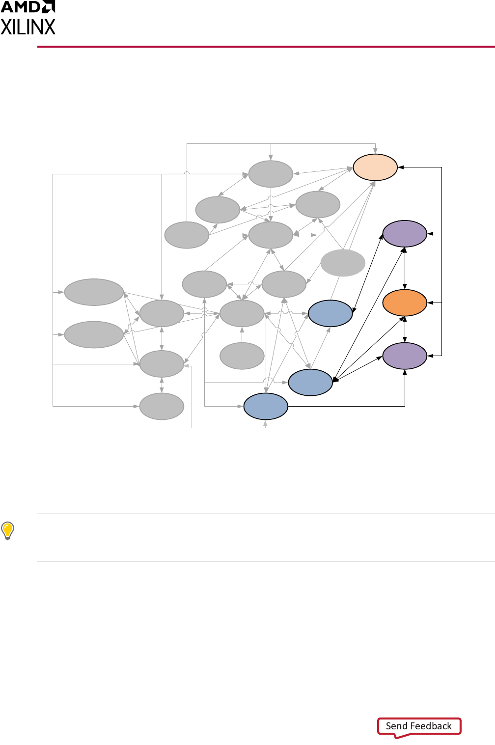
Vivado Properties Reference 142
UG912 (v2022.1) June 8, 2022 www.xilinx.com
Chapter2: Alphabetical List of First Class Objects
WIRE
Description
A WIRE is a device object used for routing connections, or NETs, on the Xilinx part. A WIRE
is a strip of interconnect metal inside a single tile. Wires connect between PIPs, tie-offs, and
SITE_PINs.
TIP: The WIRE object should not be confused with the wire entity in the Verilog files of a design. Those
wires are related to NETs in the design rather than the routing resources of the device which are defined
by the WIRE object.
Related Objects
As seen in Figure 2-33, page 119, WIRE objects are related to TILEs, NODEs, PIPs, or NETs.
You can query WIREs using a form of the following Tcl command:
get_wires -of [get_tiles INT_R_X7Y47]
X-Ref Target - Figure 2-41
Figure2‐41: WIRE Objects
Net
Pin
Port
Clock
Cell
Bel
Site/CLB
Clock
Region
Package
Pin
Bel Pin
Site Pin
Site Pip
I/O
Standard
I/O Bank
Wire
Node
Pip
Tile
Timing
Path
SLR
PkgPin
_ByteGroup
PkgPin
_Nibble
X14887-081315

Vivado Properties Reference 143
UG912 (v2022.1) June 8, 2022 www.xilinx.com
Chapter2: Alphabetical List of First Class Objects
You can also query the TILEs that WIREs are located in; or the NODEs and PIPs associated
with specific WIREs:
get_nodes -of_objects [get_wires INT_R_X7Y47/NW6BEG1]
Properties
The properties on a WIRE object can be reported with a command such as the following:
report_property -all [lindex [get_wires -of [get_nodes INT_R_X7Y47/NW6BEG1]] 0]
TIP: Due to the number of WIREs on a device, using the get_wires Tcl command without
-of_objects or -filters to narrow the results is not recommended.
The properties include the following, with example values:
Property Type Read-only Visible Value
CLASS string true true wire
COST_CODE int true true 3
ID_IN_TILE_TYPE int true true 123
IS_CONNECTED bool true true 1
IS_INPUT_PIN bool true true 0
IS_OUTPUT_PIN bool true true 0
IS_PART_OF_BUS bool true true 0
NAME string true true INT_R_X7Y47/NW6BEG1
NUM_DOWNHILL_PIPS int true true 0
NUM_INTERSECTS int true true 1
NUM_PIPS int true true 20
NUM_TILE_PORTS int true true 0
NUM_UPHILL_PIPS int true true 20
SPEED_INDEX int true true 2232
TILE_NAME string true true INT_R_X7Y47
TILE_PATTERN_OFFSET int true true 0

Vivado Properties Reference 144
UG912 (v2022.1) June 8, 2022 www.xilinx.com
Chapter 3
Key Property Descriptions
Properties Information
This chapter provides information about Xilinx
®
Vivado
®
Design Suite properties. The entry
for each property contains the following information, where applicable:
•A Description of the property, including its primary uses.
• The Xilinx FPGA Architectures supporting the property, including UltraScale™
architecture devices, except where specifically noted.
•The Applicable Objects or device resources supporting the property.
•Possible Values that can be assigned to the property.
• Syntax specifications, including Verilog, VHDL, and XDC where applicable.
• Affected Steps in the design flow where the property has influence.
• See Also cross references to related properties.
IMPORTANT: When a property is defined in both HDL code and as a constraint in the XDC file, the XDC
property takes precedence and overrides the HDL property.
For more information on the use of these properties within the Vivado Design Suite, refer to
the Vivado Design Suite User Guide: Using Constraints (UG903) [Ref 19].

Vivado Properties Reference 145
UG912 (v2022.1) June 8, 2022 www.xilinx.com
Chapter3: Key Property Descriptions
ASYNC_REG
IMPORTANT: If ASYNC_REG and IOB are both assigned to a register, the IOB property takes precedence
over ASYNC_REG and the register is placed in an ILOGIC block rather than into SLICE/CLB logic.
ASYNC_REG is an attribute that affects many processes in the Vivado tools flow. ASYNC_REG
specifies that:
• A register can receive asynchronous data on the D input pin relative to its source clock.
• A register is a synchronizing register within a synchronization chain.
During simulation, when a timing violation occurs, the default behavior is for a register
element to output an 'X', or unknown state (not a 1 or 0). When this happens, anything that
element drives will see an 'X' on its input and in turn enters an unknown state. This
condition can propagate through the design, in some cases causing large sections of the
design to become unknown, and sometimes the simulator can not recover from this state.
ASYNC_REG modifies the register to output the last known value even though a timing
violation occurs.
Vivado synthesis treats the ASYNC_REG property like the DONT_TOUCH property, and
pushes it forward in the synthesized netlist. This ensures that synthesis will not optimize
registers or surrounding logic, and that downstream tools in the design flow receive the
ASYNC_REG property for processing.
Specifying ASYNC_REG also affects optimization, placement, and routing to improve mean
time between failure (MTBF) for registers that can go metastable. If ASYNC_REG is applied,
the placer will ensure the flip-flops on a synchronization chain are placed closely together
in order to maximize MTBF. Registers that have this property that are directly connected will
be grouped and placed together into a single SLICE/CLB, assuming they have a compatible
X-Ref Target - Fig ure 3-1
Figure3‐1: Synchronizing Clock Domains
clk2
clk1
IBUF
IBUF1
I0
BUFG
BUFG1
I0
clk
C
CE
CLR
D
tc
FDCE
Q
-
snd<0>
sender
-
rcv0
receiver_1
sync 1
FDCE
C
CE
CLR
D
sync 0
FDCE
Q
C
CE
CLR
D
Q
I0
I1
0
_n0017_inv1
LUT2
IBUF
I0
BUFG
I0
en
clk
X14888-081315

Vivado Properties Reference 146
UG912 (v2022.1) June 8, 2022 www.xilinx.com
Chapter3: Key Property Descriptions
control set and the number of registers does not exceed the available resources of the
SLICE/CLB.
TIP: For UltraScale devices, mean time between failures (MTBF) can be reported for synchronizing
registers identified with ASYNC_REG using the report_synchronizer_mtbf command.
The following is a Verilog example of a two FF, or one-stage synchronizer, as shown in
Figure 3-1. The registers synchronize a signal from a separate clock domain. The
ASYNC_REG property is attached to synchronizing stages with a value of TRUE:
(* ASYNC_REG = "TRUE" *) reg sync_0, sync_1;
always @(posedge clk) begin
sync_1 <= sync_0;
sync_0 <= en;
. . .
TIP: The ASYNC_REG property can also be used with SystemVerilog logic syntax:
(* ASYNC_REG = "TRUE" *) logic sync_0, sync_1;
-or-
(* ASYNC_REG = "TRUE" *) output logic sync_0, sync_1,
With the ASYNC_REG property, the registers are grouped so that they are placed as closely
together as possible.
X-Ref Target - Fig ure 3-2
Figure3‐2: Grouping Registers

Vivado Properties Reference 147
UG912 (v2022.1) June 8, 2022 www.xilinx.com
Chapter3: Key Property Descriptions
Architecture Support
All architectures.
Applicable Objects
• Signals declared in the source RTL
• Instantiated register cells (get_cells)
°
Registers (FD, FDCE, FDPE, FDRE, FDSE)
Values
• TRUE: The register is part of a synchronization chain. It will be preserved through
implementation, placed near the other registers in the chain and used for MTBF
reporting.
• FALSE: The register can be optimized away, or absorbed into a block such as SRL, DSP,
or RAMB. No special simulation, placement, or routing rules will be applied to it
(default).
Syntax
Verilog Syntax
Place the Verilog attribute immediately before the instantiation or reg declaration of a
register:
(* ASYNC_REG = "{TRUE|FALSE}" *)
Verilog Syntax Example
// Designates sync_regs as receiving asynchronous data
(* ASYNC_REG = "TRUE" *) reg [2:0] sync_regs;
VHDL Syntax
Declare and specify the VHDL attribute as follows for inferred logic:
attribute ASYNC_REG : string;
attribute ASYNC_REG of name: signal is "TRUE";
Or, specify the VHDL attribute as follows for instantiated logic:
attribute ASYNC_REG of name: label is "TRUE";
Where name is:
• The declared signal that will be inferred to a synchronizer register, or

Vivado Properties Reference 148
UG912 (v2022.1) June 8, 2022 www.xilinx.com
Chapter3: Key Property Descriptions
• The instance name of an instantiated register
VHDL Syntax Example
attribute ASYNC_REG : string;
signal sync_regs : std_logic_vector(2 downto 1);
-- Designates sync_regs as receiving asynchronous data
attribute ASYNC_REG of sync_regs: signal is "TRUE";
XDC Syntax
set_property ASYNC_REG value [get_cells <instance_name>]
Where
• <instance_name> is a register cell.
XDC Syntax Example
# Designates sync_regs as receiving asynchronous data
set_property ASYNC_REG TRUE [get_cells sync_regs*]
Affected Steps
• launch_xsim
•Synthesis
•Place Design
•Route Design
• Phys Opt Design
•Power Opt Design
•report_drc
• write_verilog
•write_vhdl
See Also
IOB, page 260

Vivado Properties Reference 149
UG912 (v2022.1) June 8, 2022 www.xilinx.com
Chapter3: Key Property Descriptions
AUTO_INCREMENTAL_CHECKPOINT
The AUTO_INCREMENTAL_CHECKPOINT property is a boolean property that enables or
disables the automatic incremental implementation flow, to reuse the placement and
routing from an earlier iteration of the current design. This property works with the
INCREMENTAL_CHECKPOINT property to manage incremental implementation in the
Vivado tools. Refer to this link in the Vivado Design Suite User Guide: Implementation
(UG904) [Ref 20] for more information.
TIP: The AUTO_INCREMENTAL_CHECKPOINT property is only supported in the Vivado tools
project-mode. To reuse prior placement and routing results in non-project mode use the
read_checkpoint -incremental command.
The incremental implementation flow can be configured in one of three ways:
• Automatic reuse of the prior placement and routing of the current design. Enable the
AUTO_INCREMENTAL_CHECKPOINT property.
• Manual reuse of the placement and routing data from a prior implementation of a
specified design checkpoint. Disable the AUTO_INCREMENTAL_CHECKPOINT property,
and specify the INCREMENTAL_CHECKPOINT property.
• Disabled so there is no incremental implementation. Disable the
AUTO_INCREMENTAL_CHECKPOINT property, and do not specify the
INCREMENTAL_CHECKPOINT property.
Architecture Support
All architectures.
Applicable Objects
• Vivado implementation run objects (get_runs)
Values
• 1: Enables the automatic incremental implementation design flow. This lets the Vivado
placement and routing tools reuse the placement and routing from prior
implementations of the current design, to speed processing of the design.
• 0: Disables the automatic incremental implementation design flow. This is the default
setting.

Vivado Properties Reference 150
UG912 (v2022.1) June 8, 2022 www.xilinx.com
Chapter3: Key Property Descriptions
Syntax
Verilog and VHDL Syntax
Not applicable
XDC Syntax
set_property AUTO_INCREMENTAL_CHECKPOINT 1 [get_runs <impl_run> \
-filter {IS_IMPLEMENTATION}]
Where:
• <impl_run> is the name of an implementation run in the current design or project.
TIP: You can use the -filter {IS_IMPLEMENTATION} option for the get_runs command to get
just implementation runs.
XDC Syntax Example
set_property AUTO_INCREMENTAL_CHECKPOINT 1 [get_runs * -filter {IS_IMPLEMENTATION}]
Affected Steps
• Implementation
See Also
INCREMENTAL_CHECKPOINT, page 254

Vivado Properties Reference 151
UG912 (v2022.1) June 8, 2022 www.xilinx.com
Chapter3: Key Property Descriptions
AUTOPIPELINE_GROUP
The AUTOPIPELINE_GROUP property (see AUTOPIPELINE_MODULE,
AUTOPIPELINE_INCLUDE, AUTOPIPELINE_LIMIT) is used to define a group of nets as the
objects of auto-pipelining optimization. When this optimization feature is triggered, it will
insert and place the additional pipeline stages based on setup timing slack and SLR
distance. See “Auto-Pipelining” in Vivado Design Suite User Guide: Implementation (UG904)
[Ref 20] for more information.
Architecture Support
UltraScale, UltraScale+, Versal™ ACAP architectures.
Applicable Objects
• Nets (get_nets)
• Cells (get_cells)
Each single net should be directly driven by a flip-flop, and the fanout load can only be 1.
Value
<group_name>: This is a unique string value that can be assigned to one or more nets. The
placer will take the specified objects as one whole group to implement the auto-pipeline
insertion. The signals with a same auto-pipeline group name must receive an equal number
of auto-inserted pipeline flip-flops.
Syntax
VHDL Example Syntax
attribute autopipeline_group : string;
signal mywire: std_logic_vector(2 downto 1);
attribute autopipeline_group of mywire: signal is "group_name";
Verilog Example Syntax
(* autopipeline_group="group_name"*) wire mywire;
XDC Example Syntax
set_property AUTOPIPELINE_GROUP group_name [get_nets mywire]


Vivado Properties Reference 153
UG912 (v2022.1) June 8, 2022 www.xilinx.com
Chapter3: Key Property Descriptions
AUTOPIPELINE_MODULE
The AUTOPIPELINE_MODULE property establishes a separate name-space for all group
names defined throughout sub-hierarchies. It must be set on the hierarchy which includes
the nets tagged with AUTOPIPELINE_GROUP and AUTOPIPELINE_LIMIT. It also must be used
when a module with auto-pipelining properties is instantiated several times in the design.
See “Auto-Pipelining” in Vivado Design Suite User Guide: Implementation (UG904) [Ref 20]
for more information.
Architecture Support
UltraScale, UltraScale+, Versal ACAP.
Applicable Objects
• Hierarchical cells
Value
• <True>: The auto-pipelining insertion happens in the specified module.
• <False>: No auto-pipelining insertion happens in the specified module. This is the
default mode.
Syntax
VHDL Example Syntax
attribute autopipeline_module : boolean;
attribute autopipeline_module of beh: architecture is "true";
Verilog Example Syntax
(* autopipeline_module = “true” *) module test(in1, in2, clk, out1)
XDC Example Syntax
set_property AUTOPIPELINE_MODULE TRUE [get_cells test]
Affected Steps
•Place Design
• Phys Opt Design

Vivado Properties Reference 154
UG912 (v2022.1) June 8, 2022 www.xilinx.com
Chapter3: Key Property Descriptions
AUTOPIPELINE_INCLUDE
The AUTOPIPELINE_INCLUDE property specifies the name of another
AUTOPIPELINE_GROUP to include when applying the AUTOPIPELINE_LIMIT. The normal
usage scenario is in the forward and response shakehands protocal paths, one direction is
defined as a “forward” group using AUTOPIPELINE_GROUP, and the other direction is
defined as a primary “response” group using AUTOPIPELINE_GROUP, while adding reference
to the forward group, so the round-trip path would share the maximum limit as defined.
Architecture Support
UltraScale, UltraScale+, Versal ACAP.
Applicable Objects
•Nets (get_nets)
• Cells (get_cells)
Each single net should be directly driven by a flip-flop, and the fanout load can only be 1.
Value
• <group_name>: This is a unique string value that can be assigned to one or more nets.
The signals with a same auto-pipeline include group name must receive an equal
number of auto-inserted pipeline flip-flops.
Syntax
VHDL Example Syntax
attribute autopipeline_include : string;
attribute autopipeline_group : string;
attribute autopipeline_limit : integer;
signal mywire: std_logic_vector(2 downto 1);
signal mybus: std_logic_vector(2 downto 1);
attribute autopipeline_group of mywire: signal is "sub_group";
attribute autopipeline_group of mybus: signal is "primary_group";
attribute autopipeline_include of mybus: signal is "sub_group";
attribute autopipeline_limit of mybus: signal is "12”;
Verilog Example Syntax
(* autopipeline_group="sub_group”*) wire mywire;
(* autopipeline_group="primary_group", autopipeline_limite= 12,
autopipeline_include="sub_group"*) wire mybus;

Vivado Properties Reference 155
UG912 (v2022.1) June 8, 2022 www.xilinx.com
Chapter3: Key Property Descriptions
XDC Example Syntax
set_property AUTOPIPELINE_GROUP primary_group [get_nets mywire]
set_property AUTOPIPELINE_INCLUDE sub_group [get_nets mywire]
The sub_group is included in the primary_group, and shares the maximum limit of 12
stages.
Affected Steps
•Place Design
• Phys Opt Design

Vivado Properties Reference 156
UG912 (v2022.1) June 8, 2022 www.xilinx.com
Chapter3: Key Property Descriptions
AUTOPIPELINE_LIMIT
The AUTOPIPELINE_LIMIT property specifies the maximum limitation for the pipeline stages
to be inserted by the optimization techniques.
Architecture Support
UltraScale, UltraScale+, Versal ACAP.
Applicable Objects
• Nets (get_nets)
• Cells (get_cells)
Each single net should be directly driven by a flip-flop, and the fanout load can only be 1.
Value
• <N>: This is an integer number with a limit of 24.
Syntax
VHDL Example Syntax
attribute autopipeline_limit : integer;
signal mywire: std_logic_vector(2 downto 1);
attribute autopipeline_limit of mywire: signal is "12";
Verilog Example Syntax
(* autopipeline_limit="12"*) wire mywire;
XDC Example Syntax
set_property AUTOPIPELINE_LIMIT 12 [get_nets mywire]
Affected Steps
•Place Design
• Phys Opt Design

Vivado Properties Reference 157
UG912 (v2022.1) June 8, 2022 www.xilinx.com
Chapter3: Key Property Descriptions
BEL
BEL specifies the placement of a leaf-level Cell within a SLICE/CLB, or other site which can
contain multiple cells. BEL is typically used with an associated LOC property to specify the
exact placement of a register or LUT.
IMPORTANT: The BEL property or constraint must be defined prior to the LOC property or constraint, or
a placement error is returned.
Architecture Support
All architectures.
Applicable Objects
• Cells (get_cells)
°
Register (FD, FDCE, FDPE, FDRE, FDSE)
°
LUT (LUT1, LUT2, LUT3, LUT4, LUT5, LUT6, LUT6_2)
°
SRL (SRL16E, SRLC32E)
°
LUTRAM (RAM32X1S, RAM64X1S)
°
Configuration Components (BSCAN, ICAP, etc.)
Values
•BEL = <name> BEL names can take many different forms depending on the specific
logic contents of the BEL. BEL names can also hierarchically include the SITE name for
the BEL. For instance, some valid BEL names are BSCAN_X0Y0/BSCAN, and
SLICE_X1Y199/A5FF.
Syntax
Verilog Syntax
Place the Verilog attribute immediately before the instantiation. The Verilog attribute can
also be placed before the reg declaration of an inferred register, SRL, or LUTRAM.
(* BEL = "site_name" *)
Verilog Syntax Example
// Designates placed_reg to be placed in FF site A5FF

Vivado Properties Reference 158
UG912 (v2022.1) June 8, 2022 www.xilinx.com
Chapter3: Key Property Descriptions
(* BEL = "A5FF" *) reg placed_reg;VHDL Syntax
Declare the VHDL attribute as follows:
attribute BEL : string;
For an instantiated instance, specify the VHDL attribute as follows:
attribute BEL of instance_name : label is "site_name";
Where
• instance_name is the instance name of an instantiated register, LUT, SRL, or LUTRAM.
VHDL Syntax Example
-- Designates instantiated register instance placed_reg to be placed in FF site A5FF
attribute BEL of placed_reg : label is "A5FF";
For an inferred instance, specify the VHDL attribute as follows:
attribute BEL of signal_name : signal is "site_name";
Where
• signal_name is the signal name of an inferred register, LUT, SRL, or LUTRAM.
VHDL Syntax Example
-- Designates instantiated register instance placed_reg to be placed in FF site A5FF
attribute BEL of placed_reg : signal is "A5FF";
XDC Syntax
set_property BEL site_name [get_cells instance_name]
Where
• instance_name is a register, LUT, SRL, or LUTRAM, or other cell instance.
XDC Syntax Example
# Designates placed_reg to be placed in FF site A5FF
set_property BEL A5FF [get_cells placed_reg]
Affected Steps
• Design Floorplanning
•Place Design


Vivado Properties Reference 160
UG912 (v2022.1) June 8, 2022 www.xilinx.com
Chapter3: Key Property Descriptions
BLACK_BOX
The BLACK_BOX attribute is a useful debugging attribute that can turn a whole level of
hierarchy off and enable synthesis to create a black box for that module or entity. When the
attribute is found, even if there is valid logic for a module or entity, Vivado synthesis creates
a black box for that level. This attribute can be placed on a module, entity, or component.
IMPORTANT: Because this attribute affects the synthesis compiler, it can only be set in the RTL.
For more information regarding coding style for Black Boxes, refer to this link in the Vivado
Design Suite User Guide: Synthesis (UG901) [Ref 18].
Architecture Support
• All architectures.
Applicable Objects
• Modules, entities, or components in the source RTL.
Values
• YES | TRUE: Specifies that the module or entity should be viewed as a black box and
not expanded as part of the elaborated or synthesized design.
IMPORTANT: To disable the black box feature, remove the BLACK_BOX attribute from the RTL module
or entity. Do not simply set the attribute to NO or FALSE.
Syntax
Verilog Syntax
In Verilog, the BLACK_BOX attribute on the module does not require a value. Its presence
defines a black box.
(* black_box *) module test(in1, in2, clk, out1);
VHDL Syntax
attribute black_box : string;
attribute black_box of beh : architecture is "yes";


Vivado Properties Reference 162
UG912 (v2022.1) June 8, 2022 www.xilinx.com
Chapter3: Key Property Descriptions
BLI
The Boundary Logic Interface (BLI) constraint instructs the Vivado placer to place a flip flop cell into
the BLI resources that exist at the interface between Programmable Logic and XPIO/AIE resources.
BLI resources can help optimize the timing of the interface. The Vivado placer will only place the
flip-flop cell into the BLI resource if connectivity, control set, and initial value criteria are met.
Architecture Support
Versal ACAP
Applicable Objects
• Flip-flop cells (get_cells) connected to applicable XPIO or AI Engine primitives.
Values
• TRUE: The flip-flop cell will be placed into the BLI resource if connectivity, control set, and initial
value criteria are met.
• FALSE: The flip-flop cell will not be placed into the BLI resource (default).
• AUTO: Currently unsupported.
Syntax
Verilog and VHDL Syntax
Not applicable
XDC Syntax
set_property BLI <TRUE | FALSE> [get_cells <ff_cells>]
XDC Syntax Examples
# Use BLI Flip flop
set_property BLI TRUE [get_cells myHier/myBliFlop]
Affected Steps
• Implementation
See Also
• Versal ACAP AI Engine Architecture Manual (AM009) [Ref 33]
• Versal ACAP SelectIO Resources Architecture Manual (AM010) [Ref 34]

Vivado Properties Reference 163
UG912 (v2022.1) June 8, 2022 www.xilinx.com
Chapter3: Key Property Descriptions
BLOCK_SYNTH
The BLOCK_SYNTH property lets you assign synthesis properties to an instance of a
hierarchical module in the design, to provide a greater degree of control over global
synthesis. With BLOCK_SYNTH you can specify different optimizations for two different
instances of the same module, and process them during global synthesis.
By setting a BLOCK_SYNTH on an instance, you will be affecting that instance and
everything below it. For example, if a hierarchical module has other modules nested within
it, those modules are also affected by the BLOCK_SYNTH property. However, you can also
assign another BLOCK_SYNTH property to the nested module to change its settings, or
restore it to the default value.
When working with IP, you can use the BLOCK_SYNTH property when the IP is specified for
global synthesis.
IMPORTANT: If the IP is specified for out-of-context (OOC) synthesis, the BLOCK_SYNTH property is
ignored.
You can use the block-level synthesis strategy to synthesize different levels of hierarchy with
different synthesis options in a top-down flow. You can specify constraints for the full
design, and also specify unique constraints for specific instances of hierarchical modules.
For more information on block-level synthesis, refer to this link in the Vivado Design Suite
User Guide: Synthesis (UG901) [Ref 18].
Architecture Support
• All architectures.
Applicable Objects
• Hierarchical modules (get_cells)
IMPORTANT: Set the property on a cell instance, and not on an entity or module name.
Values
• BLOCK_SYNTH.<option_name>: Indicates that the module instance should be
synthesized with the specified parameters or options. The list of options that can be
specified can be found in the Vivado Design Suite User Guide: Synthesis (UG901)
[Ref 18].

Vivado Properties Reference 164
UG912 (v2022.1) June 8, 2022 www.xilinx.com
Chapter3: Key Property Descriptions
Syntax
Verilog and VHDL Syntax
Not applicable
XDC Syntax
Set the BLOCK_SYNTH property in the XDC file using the following syntax:
set_property BLOCK_SYNTH.<option_name> <value> [get_cells <instance_name>]
Where:
• <option_name> specifies the option to be defined.
• <value> specifies the value of the option.
• <instance_name> specifies the instance name of an hierarchical cell, block, or IP, to
apply the property to.
For example, you can define the following in an XDC file:
set_property BLOCK_SYNTH.RETIMING 1 [get_cells U1]
set_property BLOCK_SYNTH.STRATEGY {AREA_OPTIMIZED} [get_cells U2]
set_property BLOCK_SYNTH.STRATEGY {AREA_OPTIMIZED} [get_cells U3]
set_property BLOCK_SYNTH.STRATEGY {DEFAULT} [get_cells U3/inst1]
Affected Steps
•Synthesis


Vivado Properties Reference 166
UG912 (v2022.1) June 8, 2022 www.xilinx.com
Chapter3: Key Property Descriptions
CARRY_REMAP
The opt_design -carry_remap option lets you remap single CARRY* cells into LUTs to
improve the routing results of the design. When using the -carry_remap option, only
single-stage carry chains are converted to LUTs. The CARRY_REMAP property lets you
specify carry chains of greater length to be converted during optimization.
You can control the conversion of individual carry chains of any length by using the
CARRY_REMAP cell property. The CARRY_REMAP property value is an integer that specifies
the maximum carry chain length to be mapped to LUTs. The CARRY_REMAP property is
applied to CARRY* primitives within a chain, and each cell must have the same value to be
converted to LUTs during optimization.
IMPORTANT: Each CARRY cell in a carry chain must have the same CARRY_REMAP value. If at least one
of the cascaded cells cannot be remapped due to presence of the DONT_TOUCH property, then the
entire chain cannot be remapped. A warning will be issued when this occurs.
Refer to the Vivado Design Suite User Guide: Implementation (UG904) [Ref 20] for more
information on optimization.
Architecture Support
• All architectures.
Applicable Objects
•CARRY Cells (get_cells)
Value
• <VALUE>: Specify an integer value that indicates the length of the carry chain that can
be converted to LUTs during opt_design.
°
CARRY_REMAP=0: Do not remap.
°
CARRY_REMAP=1: Remap single CARRY cells that are not part of a carry chain.
°
CARRY_REMAP=2: Remap carry chain with length of 2 or less.
Syntax
Verilog and VHDL Syntax
Not applicable

Vivado Properties Reference 167
UG912 (v2022.1) June 8, 2022 www.xilinx.com
Chapter3: Key Property Descriptions
XDC Syntax
set_property CARRY_REMAP <value> <objects>
XDC Syntax Example
The following assigns a CARRY_REMAP property to all CARRY8 primitives:
set_property CARRY_REMAP 2 [get_cells -hier -filter {ref_name == CARRY8}]
Affected Steps
• Logic Optimization (Opt Design)
See Also
DONT_TOUCH, page 209
LUT_REMAP, page 300
MUXF_REMAP, page 314

Vivado Properties Reference 168
UG912 (v2022.1) June 8, 2022 www.xilinx.com
Chapter3: Key Property Descriptions
CASCADE_HEIGHT
The CASCADE_HEIGHT attribute is an integer used to describe the length of the cascade
chains of large RAMS that are put into block RAMs. When a RAM that is larger than a single
block RAM is described, the Vivado synthesis tool determines how it must be configured.
Often, the tool chooses to cascade the block RAMs that it creates. This attribute can be used
to shorten or limit the length of the chain. A value of 0 or 1 for this attribute effectively
turns off any cascading of block RAMs.
This attribute can be placed on the RAM in question in the RTL source files, or in an XDC
file, to drive synthesis.
Architecture Support
UltraScale and UltraScale+ architectures.
Applicable Objects
• RAM Cells (get_cells)
Values
• <VALUE>: Specify an integer.
Syntax
Verilog Syntax
(* cascade_height = 4 *) reg [31:0] ram [(2**15) - 1:0];
VHDL Syntax
attribute cascade_height : integer;
attribute cascade_height of ram : signal is 4;
XDC Syntax
set_property CASCADE_HEIGHT 4 [get_cells my_RAM_reg]
Affected Steps
•Synthesis

Vivado Properties Reference 169
UG912 (v2022.1) June 8, 2022 www.xilinx.com
Chapter3: Key Property Descriptions
CELL_BLOAT_FACTOR
The CELL_BLOAT_FACTOR property lets you specify the addition of “whitespace” or
increased cell spacing to increase placement distance between the cells of a hierarchical
module. The Vivado placer will space out the cells in the module to improve routing results
of the design.
You can use cell bloating, when the placement of cells from a module is close together and
causing congestion, to insert whitespace during the placement step. This leads to a lower
density of cells in a given area of the die, which can reduce congestion by increasing
available routing resources. This technique is particularly effective in small, congested areas
of relatively high-performance logic.
TIP: The unused logic between cells of a module can be used by the Vivado placer for other cells that
are not contained in the hierarchical module.
To use cell bloating, apply the CELL_BLOAT_FACTOR property to cells and set the value to
LOW, MEDIUM, or HIGH.
HIGH is the recommended setting when working with smaller modules of several hundred
cells. Using cell bloating on larger modules might force the placed cells of the module to be
too far apart.
IMPORTANT: If the device already uses too many routing resources, cell bloating is not recommended.
Architecture Support
All architectures.
Applicable Objects
• Cells (get_cells)
Value
• LOW | MEDIUM | HIGH: Specifies the relative spacing between the cells of an hierarchical
module.
TIP: The property can be applied to both hierarchical and leaf level cells. However, it is recommended
to apply the property to hierarchical cells ONLY for better compile time and memory consumption.

Vivado Properties Reference 170
UG912 (v2022.1) June 8, 2022 www.xilinx.com
Chapter3: Key Property Descriptions
Syntax
Verilog and VHDL Syntax
Not applicable
XDC Syntax
set_property CELL_BLOAT_FACTOR <value> <objects>
XDC Syntax Example
The following assigns a CELL_BLOAT_FACTOR property to the cpuEngine module:
set_property CELL_BLOAT_FACTOR high [get_cells { cpuEngine }]
Affected Steps
• Placement (Place Design)
• Routing (Route Design)

Vivado Properties Reference 171
UG912 (v2022.1) June 8, 2022 www.xilinx.com
Chapter3: Key Property Descriptions
CFGBVS
Xilinx devices support configuration interfaces with 3.3V, 2.5V, 1.8V, or 1.5V I/O. The
configuration interfaces include the JTAG pins in bank 0, the dedicated configuration pins
in bank 0, and the pins related to specific configuration modes in bank 14 and bank 15 in 7
series devices, and bank 65 in the UltraScale architecture.
To support the appropriate configuration interface voltage on bank 0, the Configuration
Bank Voltage Select pin (CFGBVS) must be set to VCCO_0 or GND in order to configure I/O
Bank 0 for either 3.3V/2.5V or 1.8V/1.5V operation respectively. The CFGBVS is a logic input
pin referenced between VCCO_0 and GND. When the CFGBVS pin is connected to the
VCCO_0 supply, the I/O on bank 0 support operation at 3.3V or 2.5V during configuration.
When the CFGBVS pin is connected to GND, the I/O in bank 0 support operation at 1.8V or
1.5V during configuration.
The CFGBVS pin setting determines the I/O voltage support for bank 0 at all times. For 7
series devices in which bank 14 and bank 15 are the HR bank type, or bank 65 in UltraScale
architecture, the CFGBVS pin and the respective CONFIG_VOLTAGE property determine the
I/O voltage support during configuration.
IMPORTANT: When the CFGBVS pin is set to GND for 1.8V/1.5V I/O operation, the VCCO_0 supply and
I/O signals to Bank 0 must be 1.8V (or lower) to avoid damage to the XIlinx FPGA.
Refer to the 7 Series FPGAs Configuration User Guide (UG470) [Ref 1], or the UltraScale
Architecture Configuration User Guide (UG570) [Ref 7] for more information on
Configuration Bank Voltage Select.
The Report DRC command checks the CFGBVS and CONFIG_VOLTAGE properties to
determine the compatibility of CONFIG_MODE setting on the current design.
Architecture Support
All architectures.
Applicable Objects
•Designs (current_design)
Values
• VCCO: Configure I/O Bank 0 for 3.3V/2.5V operation.
• GND: Configure I/O Bank 0 for 1.8V/1.5V operation.

Vivado Properties Reference 172
UG912 (v2022.1) June 8, 2022 www.xilinx.com
Chapter3: Key Property Descriptions
Syntax
Verilog and VHDL Syntax
Not applicable
XDC Syntax
set_property CFGBVS [VCCO | GND] [current_design]
XDC Syntax Example
# Configure I/O Bank 0 for 3.3V/2.5V operation
set_property CFGBVS VCCO [current_design]
Affected Steps
• I/O Planning
•Report DRC
• Write Bitstream
See Also
CONFIG_MODE, page 187
CONFIG_VOLTAGE, page 189

Vivado Properties Reference 173
UG912 (v2022.1) June 8, 2022 www.xilinx.com
Chapter3: Key Property Descriptions
CLOCK_BUFFER_TYPE
By default, Vivado synthesis infers an input buffer and global clock buffer (IBUF/BUFG)
combination for clocks ports. However, you can use the IO_BUFFER_TYPE and the
CLOCK_BUFFER_TYPE properties together to direct the Vivado synthesis tool to change the
default buffer types, such as an IBUF/BUFR pair, or no input buffer with a BUFIO clock
buffer; or to eliminate the buffers altogether.
Mandatory logic optimization (MLO), which occurs at the beginning of link_design and
opt_design supports the use of the CLOCK_BUFFER_TYPE property to insert global clock
buffers. Supported values are BUFG for 7 series, and BUFG and BUFGCE for UltraScale,
UltraScale+, and Versal devices. The value NONE can be used for all architectures to
suppress global clock buffer insertion through MLO and opt_design. For the values BUFG
and BUFGCE, opt_design and MLO inserts the corresponding buffer type to drive the
specified net.
The CLOCK_BUFFER_TYPE property indicates what type of clock buffer to infer for the
specified net or port objects. The IO_BUFFER_TYPE property indicates whether to infer an
input or output buffer for the port.
TIP: The use of the CLOCK_BUFFER_TYPE property implies a KEEP on the target net, which preserves
the net name and prevents removing the net through RTL optimization.
CLOCK_BUFFER_TYPE can be defined in the RTL or in the XDC. When specified in the RTL, the
property can be attached to a port. After synthesis, the property CLOCK_BUFFER_TYPE should be
attached to the net driven by the input buffer.
Note: MAX_FANOUT does not work on nets with CLOCK_BUFFER_TYPE
Applicate Objects:
• Ports (get_ports): Apply CLOCK_BUFFER_TYPE to any top-level clock port to describe what type
of clock buffer to use, or to use no clock buffer. For 7 series, UltraScale and Ultra Scale Plus, the
property can only be set on ports inside RTL and won’t be used by opt_design when set on ports
through XDC. For Versal, opt_design only supports CLOCK_BUFFER_TYPE on ports through XDC
for OOC implementation. For any other flow, the property should be set on the net driven by the
top-level port.
•Nets (get_nets): Apply CLOCK_BUFFER_TYPE to any signal connected to a top-level
clock port
(synthesis) or any net (logic optimization) to describe what type of clock buffer to
use, or to use no clock buffer.
Values
• BUFGCE, BUFG, BUFH, BUFIO, BUFMR, BUFR: Directs the tool to infer the specified clock
buffer for clock ports or nets.

Vivado Properties Reference 174
UG912 (v2022.1) June 8, 2022 www.xilinx.com
Chapter3: Key Property Descriptions
• NONE: Directs the tool to not infer any clock buffers for the clocks.
Note:
Use with IO_BUFFER_TYPE “NONE” to prevent Vivado synthesis from inferring any buffers.
Syntax
Verilog Syntax
(* clock_buffer_type = "none" *) input clk1;
VHDL Syntax
entity test is port(
in1 : std_logic_vector (8 downto 0);
clk : std_logic;
out1 : std_logic_vector(8 downto 0));
attribute clock_buffer_type : string;
attribute clock_buffer_type of clk: signal is "BUFR";
end test;
XDC Syntax
set_property CLOCK_BUFFER_TYPE BUFMR [get_nets <net_name>]
Affected Steps
•Synthesis
•Opt Design
See Also
IO_BUFFER_TYPE, page 258

Vivado Properties Reference 175
UG912 (v2022.1) June 8, 2022 www.xilinx.com
Chapter3: Key Property Descriptions
CLOCK_DEDICATED_ROUTE
The CLOCK_DEDICATED_ROUTE property is enabled (TRUE) by default, and ensures that
clock resource placement DRCs are considered error conditions that must be corrected
prior to routing or bitstream generation. CLOCK_DEDICATED_ROUTE=FALSE downgrades
the placement DRC to a warning and lets the Vivado router use fabric routing to connect
from a clock-capable IO (CCIO) to a global clock resource such as an MMCM.
CAUTION! Setting CLOCK_DEDICATED_ROUTE to FALSE can result in sub-optimal clock delays,
resulting in potential timing violations and other issues.
External user clocks must be brought into the FPGA on differential clock pin pairs called
clock-capable inputs (CCIO). These CCIOs provide dedicated, high-speed routing to the
internal global and regional clock resources to guarantee timing of various clocking
features. Refer to the 7 Series FPGAs Clocking Resources User Guide (UG472) [Ref 3], or the
UltraScale Architecture Clocking Resources User Guide (UG572) [Ref 9] for more information
on clock placement rules.
The CLOCK_DEDICATED_ROUTE property is generally used when it becomes necessary to
place clock components in such a way as to take clock routing off of the dedicated clock
trees in the target FPGA, and use standard routing channels. If the dedicated routes are not
available, setting CLOCK_DEDICATED_ROUTE to FALSE demotes a clock placement DRC
from an ERROR to a WARNING when a clock source is placed in a sub-optimal location
compared to its load clock buffer.
Architecture Support
All architectures.
Applicable Objects
•Nets (get_nets) directly connected to the input of a global clock buffer (BUFG,
BUFGCE, BUFGMUX, BUGCTRL).
IMPORTANT: CLOCK_DEDICATED_ROUTE must be set on a net segment at the highest level of design
hierarchy, or the top-level net.

Vivado Properties Reference 176
UG912 (v2022.1) June 8, 2022 www.xilinx.com
Chapter3: Key Property Descriptions
Values
• 7 series devices
°
TRUE: Default clock placement and routing.
°
BACKBONE: Clock driver and load(s) must be placed in the same Clock Management
Tile (CMT) column. The clock routing still uses dedicated global clock routing
resources.
°
FALSE: Clock driver and load(s) can be placed anywhere in the device. The clock net
can be routed with both global clock routing resources, and standard fabric routing
resources. This can adversely affect the timing and performance of the clock net.
• UltraScale architecture
°
TRUE: Default clock placement and routing.
°
SAME_CMT_COLUMN (BACKBONE can also be used): Clock driver and load(s) must
be placed in the same Clock Management Tile (CMT) column. The clock routing
uses dedicated global clock routing resources.
°
ANY_CMT_COLUMN: Clock driver and load(s) can be placed in any CMT column and
the net uses dedicated global clock routing resources. Note that this option is not
available in 7 series devices.
°
FALSE: Clock driver and load(s) can be placed anywhere in the device. The clock net
can be routed with both global clock routing resources, and standard fabric routing
resources. This can adversely affect the timing and performance of the clock net.
Syntax
Verilog and VHDL Syntax
Not applicable
XDC Syntax
set_property CLOCK_DEDICATED_ROUTE [TRUE | FALSE | BACKBONE] [get_nets net_name]
Where
• net_name is the signal name directly connected to the input of a global clock buffer.
XDC Syntax Example
# Designates clk_net to have relaxed clock placement rules
set_property CLOCK_DEDICATED_ROUTE FALSE [get_nets clk_net]


Vivado Properties Reference 178
UG912 (v2022.1) June 8, 2022 www.xilinx.com
Chapter3: Key Property Descriptions
CLOCK_DELAY_GROUP
The CLOCK_DELAY_GROUP property identifies related clocks that have the same MMCM,
PLL, GT source, or common driver that should be balanced during placement and routing to
reduce clock skew on timing paths between the clocks.
TIP: Clock matching (via the CLOCK_DELAY_GROUP property) is intended for use with clocks from the
same MMCM, PLL, or GT source.
Architecture Support
UltraScale, UltraScale+, and Versal ACAP architectures.
Applicable Objects
•Clock net segments (get_nets) directly connected to the output of global clock
buffers (BUFG, BUFGCE, BUFGMUX, BUFGCTRL, BUFGCE_DIV, BUFG_GT) that need to be
balanced.
Values
• <name>: A unique string identifier used by the Vivado placer to match the delays on
specified clock nets.
Syntax
Verilog and VHDL Syntax
Not applicable
XDC Syntax
set_property CLOCK_DELAY_GROUP <name> [get_nets <clk_nets>]
set_property CLOCK_DELAY_GROUP <name> [get_nets -of_objects [get_pins <clock_buffer>/O]
Where
• <name> is the unique name to associate with the specified clock nets.
• <clk_nets> is a list of clock nets directly connected to the output of global clock
buffers, that are driven by a common cell, such as an MMCM for example.
XDC Syntax Example
# Define a clock group to reduce skew between the nets.


Vivado Properties Reference 180
UG912 (v2022.1) June 8, 2022 www.xilinx.com
Chapter3: Key Property Descriptions
CLOCK_LOW_FANOUT
CLOCK_LOW_FANOUT is a boolean property that can be assigned to clocks that have a small
number of loads and that should be contained in a single clock region. The property is
assigned to clock nets driven by a global clock buffer or a set of flip flops driven by a global
clock buffer.
TIP: A global clock buffer is a BUFGCE, BUFGCE_DIV, BUFGCTRL, BUFG_GT, BUFG_PS, or BUFG_HDIO.
When CLOCK_LOW_FANOUT is TRUE on a clock net driven by a global clock buffer, the loads
should be contained within a single clock region and be driven by global clock resources. A
load is defined as any leaf input pin on the clock network, not just sequential clock pins. For
example, LUT pins are counted as loads. If there are too many loads on the net, the Vivado
tool will return a warning and ignore the CLOCK_LOW_FANOUT property.
When CLOCK_LOW_FANOUT is TRUE on a set of flip flops driven by a BUFGCE global clock
buffer, the BUFGCE global clock buffer will be replicated and drives only the flip flops with
the setting. The flip flops are placed in a single clock region and driven by global clock
resources.
The CLOCK_LOW_FANOUT property can conflict with other clock or placement properties.
For instance, if CLOCK_DEDICATED_ROUTE is specified on the same net with any value other
than TRUE, the CLOCK_DEDICATED_ROUTE property takes precedence and
CLOCK_LOW_FANOUT is ignored with a warning, CLOCK_DELAY_GROUP will take
precedence over CLOCK_LOW_FANOUT if all of the members of the CLOCK_DELAY_GROUP
cannot be placed in a single clock region. USER_CLOCK_ROOT, LOC, and PBLOCK properties
can also create conflicts with the CLOCK_LOW_FANOUT property. In each of these cases
CLOCK_LOW_FANOUT is ignored and a warning is returned.
Architecture Support
UltraScale and UltraScale+ architectures.
Applicable Objects
•Clock nets (get_nets) connected to the output of global clock buffers that should be
constrained to a single clock region.
• Flip flop cells (get_cells) connected to the output of a BUFGCE global clock buffer. A
new BUFGCE global clock buffer is replicated in parallel with the existing BUFGCE
global clock buffer and the loads of the new BUFGCE global clock buffer are
constrained to a single clock region.

Vivado Properties Reference 181
UG912 (v2022.1) June 8, 2022 www.xilinx.com
Chapter3: Key Property Descriptions
Values
• TRUE: The clock is a low fanout net and should be constrained into a single clock
region.
• FALSE: The clock is not a low fanout signal, or should not be constrained to a single
clock region (default).
Syntax
Verilog and VHDL Syntax
Not applicable
XDC Syntax
set_property CLOCK_LOW_FANOUT TRUE [get_nets <clk_nets>]
set_property CLOCK_LOW_FANOUT TRUE [get_cells <ff_cells>]
Where
• <clk_nets> is a list of clock nets directly connected to the output of global clock
buffers, that are driven by a common cell, such as an MMCM for example.
•<ff_cells> is a list of flip flop cells directly connect to the output of a BUFGCE
global clock buffer.
XDC Syntax Example
# Define a clock group to reduce skew between the nets.
set_property CLOCK_LOW_FANOUT TRUE [get_nets -of [get_pins block/myBufg/O]]
# Define a list of Flip Flops to be driven by a separate BUFGCE and placed in a single
clock region
set_property CLOCK_LOW_FANOUT TRUE [get_cells block/myStartupCircuit/startup_reg[*]]
Affected Steps
•Opt Design
•Place Design
•report_drc
See Also
CLOCK_DEDICATED_ROUTE, page 175
CLOCK_DELAY_GROUP, page 178


Vivado Properties Reference 183
UG912 (v2022.1) June 8, 2022 www.xilinx.com
Chapter3: Key Property Descriptions
CLOCK_REGION
The CLOCK_REGION property lets you assign a clock buffer to a specific clock region of an
UltraScale device, while letting the Vivado placer assign the clock buffer to the best site
within that region.
IMPORTANT: For UltraScale devices, it is not recommended to fix a Clock Buffer to a specific site, as
you might do in clock planning a 7 series design. Instead, you can assign a Clock Buffer to a specific
CLOCK_REGION and leave the clock resources available to the Vivado placer to determine the best
clocking structure.
Architecture Support
UltraScale and UltraScale+ architectures.
Applicable Objects
• Global clock buffer cells (get_cells)
°
BUFG cells (BUFGCE, BUFGCTRL, BUFG_GT, BUFGCE_DIV)
Values
• <VALUE>: Specify the CLOCK_REGION to place the cell or cells into. The
CLOCK_REGION is specified by name as X#Y#, or as returned by the
get_clock_regions Tcl command.
Note:
Refer to Vivado Design Suite Tcl Command Reference Guide (UG835) [Ref 13] for more
information on the get_clock_regions command.
Syntax
Verilog and VHDL Syntax
Not applicable
XDC Syntax
set_property CLOCK_REGION X0Y2 [get_cells <cell>]
Where
• <cell> is an instance of a global clock buffer.

Vivado Properties Reference 184
UG912 (v2022.1) June 8, 2022 www.xilinx.com
Chapter3: Key Property Descriptions
XDC Syntax Example
User assignment of the CLOCK_RERGION would be performed in XDC as follows:
set_property CLOCK_REGION X4Y6 [get_cells {sys_clk_pll/inst/clkf_buf}]
Affected Steps
•Place Design
•report_drc
See Also
CLOCK_BUFFER_TYPE, page 173
CLOCK_ROOT, page 185

Vivado Properties Reference 185
UG912 (v2022.1) June 8, 2022 www.xilinx.com
Chapter3: Key Property Descriptions
CLOCK_ROOT
IMPORTANT: The CLOCK_ROOT property has changed from a user-definable property to a read-only
property. The user-definable property has been changed to USER_CLOCK_ROOT, which should be used
instead.
The CLOCK_ROOT property is a read-only property reflecting the current resource
assignment of the driver, or root, of the global clock net in the physical design. The
CLOCK_ROOT reflects the clock root assigned by the Vivado placer. The place and route
tools will automatically assign the clock root to achieve the best timing for the design.
The CLOCK_ROOT value should match the user-defined USER_CLOCK_ROOT property if it is
defined. The USER_CLOCK_ROOT property lets you manually assign the clock root.
TIP: If the Vivado router is run with the Explore directive, it can add additional clock roots to a net in
order to improve the quality of the results.
Architecture Support
UltraScale and UltraScale+ architectures.
Applicable Objects
• Global clock net (get_nets) directly connected to the output of a global clock buffer.
Value
•<clock_region | pblock_name>: Specifies the name of a clock region on the target
part, or a defined Pblock in the current design.
•<object>: Specifies one or more clock nets, or net segments.
Syntax
Not applicable
Affected Steps
•Placement
•Routing


Vivado Properties Reference 187
UG912 (v2022.1) June 8, 2022 www.xilinx.com
Chapter3: Key Property Descriptions
CONFIG_MODE
The CONFIG_MODE property defines which device configuration mode or modes to use for
pin allocations, DRC reporting, and bitstream generation.
IMPORTANT: COMPATIBLE_CONFIG_MODES property has been deprecated in the 2013.3 release, and
is replaced by the CONFIG_MODE property.
Xilinx FPGAs can be configured by loading application-specific configuration data, or a
bitstream, into internal memory through special configuration pins. There are two general
configuration datapaths: a serial datapath used to minimize the device pins required, and
parallel datapaths for higher performance configuration. The CONFIG_MODE property
defines which modes are used for the current design.
Refer to the 7 Series FPGAs Configuration User Guide (UG470) [Ref 1], or the UltraScale
Architecture Configuration User Guide (UG570) [Ref 7] for more information on device
configuration modes.
Architecture Support
All architectures.
Applicable Objects
•Design (current_design)
Values
TIP: Not all of the following values apply to all device architectures. Refer to the 7 Series FPGAs
Configuration User Guide (UG470) [Ref 1], or UltraScale Architecture Configuration User Guide
(UG570) [Ref 7], for more information.
•S_SERIAL
•M_SERIAL
• S_SELECTMAP
• M_SELECTMAP
•B_SCAN
• S_SELECTMAP+READBACK
• M_SELECTMAP+READBACK
• B_SCAN+READBACK

Vivado Properties Reference 188
UG912 (v2022.1) June 8, 2022 www.xilinx.com
Chapter3: Key Property Descriptions
• S_SELECTMAP32
• S_SELECTMAP32+READBACK
• S_SELECTMAP16
• S_SELECTMAP16+READBACK
•SPIx1
•SPIx2
•SPIx4
•SPIx8
•BPI8
•BPI16
Syntax
Verilog and VHDL Syntax
Not applicable
XDC Syntax
set_property CONFIG_MODE <value> [current_design]
Where <value> specifies the configuration mode.
XDC Syntax Example
# Specify using Configuration Mode Serial Peripheral Interface, 4-bit width
set_property CONFIG_MODE {SPIx4} [current_design]
Affected Steps
• I/O Planning
•Place Design
•report_drc
• Write Bitstream

Vivado Properties Reference 189
UG912 (v2022.1) June 8, 2022 www.xilinx.com
Chapter3: Key Property Descriptions
CONFIG_VOLTAGE
Xilinx devices support configuration interfaces with 3.3V, 2.5V, 1.8V, or 1.5V I/O. The
configuration interfaces include the JTAG pins in bank 0, the dedicated configuration pins
in bank 0, and the pins related to specific configuration modes in bank 14 and bank 15 in
the 7 series devices, and bank 65 in the UltraScale architecture. You can set the
CONFIG_VOLTAGE property, or VCCO_0 voltage, to 3.3, 2.5, 1.8, or 1.5.
CONFIG_VOLTAGE must be set to the correct configuration voltage, in order to determine
the I/O voltage support for the pins in bank 0. Refer to the 7 Series FPGAs Configuration
User Guide (UG470) [Ref 1], or the UltraScale Architecture Configuration User Guide (UG570)
[Ref 7] for more information on configuration voltage.
The CFGBVS pin setting determines the I/O voltage support for bank 0 at all times. For 7
series devices in which bank 14 and bank 15 are the HR bank type, or bank 65 in UltraScale
architecture, the CFGBVS pin and the respective CONFIG_VOLTAGE property determine the
I/O voltage support during configuration.
Report DRC checks are run on Bank 0, 14, and 15 in the 7 series, or 0 and 65 in the UltraScale
architecture, to determine compatibility of CONFIG_MODE settings on the current design.
DRCs are issued based on IOSTANDARD and CONFIG_VOLTAGE settings for the bank. The
configuration voltages are also used when exporting IBIS models.
Architecture Support
All architectures.
Applicable Objects
•Designs (current_design)
Values
• 1.5, 1.8, 2.5, or 3.3
IMPORTANT: For UltraScale+ devices, the CONFIG_VOLTAGE value must be 1.8.
Syntax
Verilog and VHDL Syntax
Not applicable

Vivado Properties Reference 190
UG912 (v2022.1) June 8, 2022 www.xilinx.com
Chapter3: Key Property Descriptions
XDC Syntax
set_property CONFIG_VOLTAGE {1.5 | 1.8 | 2.5 | 3.3} [current_design]
XDC Syntax Example
# Configure I/O Bank 0 for 1.8V operation
set_property CONFIG_VOLTAGE 1.8 [current_design]
Affected Steps
•Place Design
•report_drc
• Write Bitstream
See Also
CFGBVS, page 171
CONFIG_MODE, page 187

Vivado Properties Reference 191
UG912 (v2022.1) June 8, 2022 www.xilinx.com
Chapter3: Key Property Descriptions
CONTAIN_ROUTING
The CONTAIN_ROUTING property restricts the routing of signals contained within a Pblock
to use routing resources within the area defined by the Pblock. This prevents signals inside
the Pblock from being routed outside the Pblock, and increases the reusability of the
design.
By default the definition of a Pblock restricts the placement of logic assigned to the Pblock
to within the area defined by the Pblock. This property has the same effect for routing. The
CONTAIN_ROUTING property is specific to a Pblock and must come after the
create_pblock commands in an XDC file.
TIP: The use of CONTAIN_ROUTING is highly recommended on all Pblocks associated with an OOC
module in the Hierarchical Design flow. Refer to the Vivado Design Suite User Guide: Hierarchical
Design (UG905) [Ref 21] for more information.
Only signals that are entirely owned by the Pblock cells will be contained within the Pblock.
For example, if no BUFGMUX resources are found within the Pblock, paths from or to a
BUFGMUX cannot be contained.
Architecture Support
All architectures.
Applicable Objects
•PBlocks (get_pblocks)
Values
• TRUE: Contain the routing of signals inside a Pblock to the area defined by the Pblock
range.
• FALSE: Do not contain the routing of signals inside the Pblock. This is the default.
Syntax
Verilog and VHDL Syntax
Not applicable

Vivado Properties Reference 192
UG912 (v2022.1) June 8, 2022 www.xilinx.com
Chapter3: Key Property Descriptions
XDC Syntax
set_property CONTAIN_ROUTING <TRUE | FALSE> [get_pblocks <pblock_name>]
Where:
• <pblock_name> specifies the PBlock or PBlocks to apply the property to.
XDC Example
set_property CONTAIN_ROUTING true [get_pblocks pblock_usbEngine0]
set_property CONTAIN_ROUTING true [get_pblocks pblock_usbEngine1]
Affected Steps
•Routing
See Also
EXCLUDE_PLACEMENT, page 223
PBLOCK, page 328

Vivado Properties Reference 193
UG912 (v2022.1) June 8, 2022 www.xilinx.com
Chapter3: Key Property Descriptions
CONTROL_SET_REMAP
While all registers support resets and clock enables, their use can significantly affect the
end implementation in terms of performance, utilization, and power. Designs with a large
number of unique control sets can have fewer options for placement, resulting in higher
power and lower performance. The CONTROL_SET_REMAP property is placed on register
primitives to trigger a control set reduction on a specific register during logical
optimization (opt_design).
When a logic path ends at a fabric register (FD) clock enable, or synchronous set/reset, the
property on the register instructs Vivado logic optimization to map the enable or reset
signal to the data pin (D), which has a dedicated LUT connection and can be faster. If
possible, the logic is combined with an existing LUT driving the D-input to prevent the
insertion of extra levels of logic.
IMPORTANT: This optimization is automatically triggered when the CONTROL_SET_REMAP property is
detected on any register. DONT_TOUCH prevents the optimization on specified cells or hierarchy.
For more information on reducing control sets, refer to this link in the UltraFast Design
Methodology Guide for the Vivado Design Suite (UG949) [Ref 24] for more information.
Architecture Support
All architectures.
Applicable Objects
• Cells (get_cells)
Values
• ENABLE: Remaps the EN input to the D-input.
• RESET: Remaps the synchronous S or R input to the D-input.
• ALL: Same as ENABLE and RESET combined.
• NONE: do nothing. This is the default, and is the same as if the property were not set on
the cell.
Syntax
Verilog and VHDL Syntax
Not applicable

Vivado Properties Reference 194
UG912 (v2022.1) June 8, 2022 www.xilinx.com
Chapter3: Key Property Descriptions
XDC Syntax
set_property CONTROL_SET_REMAP <value> [get_cells <cell_pattern>]
XDC Syntax Example
# Specifies control set reduction based on Enable signals
set_property CONTROL_SET_REMAP ENABLE [get_cells ff*]
Affected Steps
•Opt Design
See Also
EQUIVALENT_DRIVER_OPT, page 221

Vivado Properties Reference 195
UG912 (v2022.1) June 8, 2022 www.xilinx.com
Chapter3: Key Property Descriptions
DCI_CASCADE
DCI_CASCADE defines a master-slave relationship between a set of high-performance (HP)
I/O banks. The digitally controlled impedance (DCI) reference voltage is chained from the
master I/O bank to the slave I/O banks.
DCI_CASCADE specifies which adjacent banks use the DCI Cascade feature, thereby sharing
reference resistors with a master bank. If several I/O banks in the same I/O bank column are
using DCI, and all of those I/O banks use the same VRN/VRP resistor values, the internal
VRN and VRP nodes can be cascaded so that only one pair of pins for all of the I/O banks
in the entire I/O column is required to be connected to precision resistors. DCI_CASCADE
identifies the master bank and all associated slave banks for this feature. Refer to the 7
Series FPGAs SelectIO Resources User Guide (UG471) [Ref 2], or the UltraScale Architecture
SelectIO Resources User Guide (UG571) [Ref 8] for more information.
Architecture Support
•Kintex
®
-7 devices.
• Kintex UltraScale devices.
•Virtex
®
-7 devices.
• Virtex UltraScale devices.
•Larger Zynq
®
-7000 SoC devices.
Applicable Objects
•I/O Bank (get_iobanks)
°
High Performance (HP) bank type
Values
Valid High Performance (HP) bank numbers. See the 7 Series FPGAs Packaging and Pinout
Product Specifications User Guide (UG475) [Ref 5], or the UltraScale and UltraScale+ FPGAs
Packaging and Pinouts Product Specification User Guide (UG575) [Ref 11] for more
information.
Syntax
Verilog and VHDL Syntax
Not applicable

Vivado Properties Reference 196
UG912 (v2022.1) June 8, 2022 www.xilinx.com
Chapter3: Key Property Descriptions
XDC Syntax
set_property DCI_CASCADE {slave_banks} [get_iobanks master_bank]
Where
• slave_banks is a list of the bank numbers of the slave banks.
• master_bank is the bank number of the designated master bank.
XDC Syntax Example
# Designate Bank 14 as a master DCI Cascade bank and Banks 15 and 16 as its slaves
set_property DCI_CASCADE {15 16} [get_iobanks 14]
Affected Steps
• I/O planning
•Place Design
•DRC
• Write Bitstream
•report_power

Vivado Properties Reference 197
UG912 (v2022.1) June 8, 2022 www.xilinx.com
Chapter3: Key Property Descriptions
DELAY_BYPASS
The DELAY_BYPASS property reduces the delay through the BUFIO in Xilinx 7 series FPGAs.
There is an intrinsic delay in the BUFIO to match the delay of the BUFR to allow for smooth
data transference from those domains. For 7 series devices, this property disables that
delay.
Architecture Support
7 series FPGAs.
Applicable Objects
•BUFIO (get_cells)
Values
• TRUE: Delay bypass is enabled.
• FALSE: Delay bypass is disabled (default).
Syntax
Verilog and VHDL Syntax
Not applicable
XDC Syntax
set_property DELAY_BYPASS TRUE [get_ cells <cells>]
Where
• <cells> is a list of BUFIO cells to bypass the intrinsic delay.
XDC Syntax Example
set_ property -name DELAY_ BYPASS TRUE [get_ cells clk_ bufio]
Affected Steps
• Timing Analysis

Vivado Properties Reference 198
UG912 (v2022.1) June 8, 2022 www.xilinx.com
Chapter3: Key Property Descriptions
DELAY_VALUE_XPHY
The DELAY_VALUE_XPHY property on PORT objects specifies the amount of delay to add on
an input or output path for Versal XPHY Logic Interfaces. During the early phases of
opt_design when the Advanced I/O Wizard IP is being regenerated, the
DELAY_VALUE_XPHY value will be copied from the PORT onto the XPHY instance for the
input or output path. DRCs exist in the Vivado Design Suite to ensure that the
DELAY_VALUE_XPHY value aligns to the value on the XPHY instance. In the case where you
want to update the amount of delay on an input or output path for an already implemented
design, you can apply your new value to the PORT by using the DELAY_VALUE_XPHY
property. Then, you can run the implement_xphy_cores
-update_delay_value_only command to deposit the new value onto the XPHY
instance.
Architecture Support
Versal architecture.
Applicable Objects
•Ports (get_ports)
Values
• For input ports without a cascade: 0 - 625 ps
• For input ports with a cascade: 0 - 1250 ps
• For output ports: 0 - 625 ps
Syntax
Verilog and VDHL Syntax
Not Applicable
XDC Syntax
set_property DELAY_VALUE_XPHY <value> [get_ports port_name]
Where
• port_name is a top-level port

Vivado Properties Reference 199
UG912 (v2022.1) June 8, 2022 www.xilinx.com
Chapter3: Key Property Descriptions
XDC Syntax Example
# Open a fully implemented design
open_checkpoint top_routed.dcp
# Update the delay on the input path from PORT dataIn
set_property DELAY_VALUE_XPHY 125 [get_ports dataIn]
implement_xphy_cores -update_delay_value_only
# Write a new checkpoint and device image with the updated delay
write_checkpoint top_routed_125.dcp
write_device_image top_routed_125.pdi
Affected Steps
• Timing Analysis
•Opt Design

Vivado Properties Reference 200
UG912 (v2022.1) June 8, 2022 www.xilinx.com
Chapter3: Key Property Descriptions
DIFF_TERM
The differential termination (DIFF_TERM) property supports the differential I/O standards
for inputs and bidirectional ports. It is used to enable or disable the built-in, 100 ,
differential termination. Refer to the 7 Series FPGAs SelectIO Resources User Guide (UG471)
[Ref 2] for more information.
DIFF_TERM indicates a differential termination method should be used on differential input
and bidirectional port buffers, and that the Vivado tool should add on-chip termination to
the port.
Architecture Support
7 series FPGAs.
RECOMMENDED: For UltraScale architecture devices, you should use DIFF_TERM_ADV to enable
differential termination.
Applicable Objects
•Ports (get_ports)
°
Input or bidirectional ports connected to a differential input buffer
• Applicable to elements using one of the following IOSTANDARDs:
°
LVDS, LVDS_25, MINI_LVDS_25
°
PPDS_25
°
RSDS_25
Values
• TRUE: Differential termination is enabled.
• FALSE: Differential termination is disabled (default).

Vivado Properties Reference 201
UG912 (v2022.1) June 8, 2022 www.xilinx.com
Chapter3: Key Property Descriptions
Syntax
RECOMMENDED: Use the instantiation template from the Language Templates or the Vivado Design
Suite 7 Series FPGA and Zynq-7000 SoC Libraries Guide (UG953) [Ref 25] to specify the proper syntax.
Verilog Syntax
Assign the DIFF_TERM parameter immediately before the port declaration:
(* DIFF_TERM = "TRUE" *) input PORT
Verilog Syntax Example
// Enables differential termination on the specified port
(* DIFF_TERM = "TRUE" *) input CLK;
VHDL Syntax
Declare and specify the VHDL attribute as follows:
attribute DIFF_TERM : string;
attribute DIFF_TERM of port_name : signal is "TRUE";
VHDL Syntax Example
-- Designates differential termination on the specified port
attribute DIFF_TERM of CLK : signal is "TRUE";
XDC Syntax
set_property DIFF_TERM TRUE [get_ports port_name]
Where:
• set_property DIFF_TERM can be assigned to port objects.
• port_name is an input or bidirectional port connected to a differential buffer.
XDC Syntax Example
# Enables differential termination on port named CLK_p
set_property DIFF_TERM TRUE [get_ports CLK_p]
Affected Steps
• I/O Planning
• report_ssn
•report_power


Vivado Properties Reference 203
UG912 (v2022.1) June 8, 2022 www.xilinx.com
Chapter3: Key Property Descriptions
DIFF_TERM_ADV
The advanced differential termination (DIFF_TERM_ADV) property is intended for use with
UltraScale architecture only, and is used to enable or disable the built-in, 100 , differential
termination for inputs or bidirectional ports. DIFF_TERM_ADV indicates a differential
termination method should be used on differential input and bidirectional port buffers, and
that the Vivado Design Suite should add on-chip termination to the port.
DIFF_TERM_ADV is only available for inputs and bidirectional ports and can only be used
with the appropriate V
CCO
voltage. The V
CCO
of the I/O bank must be connected to 1.8V for
HP I/O banks, and 2.5V for HR I/O banks to provide 100 of effective differential
termination. Refer to the UltraScale Architecture SelectIO Resources User Guide (UG571)
[Ref 8] for more information.
IMPORTANT: To support the migration of 7 Series designs to UltraScale architecture, the Vivado tool.
will automatically migrate the DIFF_TERM property to the DIFF_TERM_ADV property. However, in some
cases this property is not supported, and should not be specified, or should be specified as “” (NULL)
value.
Architecture Support
UltraScale devices.
Applicable Objects
•Ports (get_ports)
°
Input or bidirectional ports connected to a differential input buffer
• Applicable to objects using one of the following IOSTANDARDs:
°
LVDS, LVDS_25, MINI_LVDS_25, SUB_LVDS
°
PPDS_25
°
RSDS_25
°
SLVS_400_25, and SLVS_400_18

Vivado Properties Reference 204
UG912 (v2022.1) June 8, 2022 www.xilinx.com
Chapter3: Key Property Descriptions
Value
• TERM_100: Utilize the 100 on-chip differential termination.
• TERM_NONE: Do not utilize the on-chip differential termination (default).
Note:
The TERM_NONE value is the default value when the DIFF_TERM_ADV property is valid,
such as for supported IOSTANDARDs and voltage levels. However, where it is not supported, it
should not be specified and DIFF_TERM_ADV=TERM_NONE can result in a DRC violation. In these
cases you can set the property to a NULL value using one of the following commands:
reset_proeprty DIFF_TERM_ADV [get_ports <port_name>]
-or-
set_property DIFF_TERM_ADV "" [get_ports <port_name>]
Syntax
Verilog and VHDL Syntax
Not applicable
XDC Syntax
set_property DIFF_TERM_ADV TERM_100 [get_ports <port_name>]
Where:
• set_property DIFF_TERM_ADV can be assigned to input or bidirectional ports.
• port_name is an input or bidirectional port connected to a differential buffer.
XDC Syntax Example
# Enables differential termination on port named CLK_p
set_property DIFF_TERM_ADV TERM_100 [get_ports CLK_p]
Affected Steps
• I/O Planning
•report_drc
• report_ssn
•report_power
See Also
DIFF_TERM, page 200
IOSTANDARD, page 268

Vivado Properties Reference 205
UG912 (v2022.1) June 8, 2022 www.xilinx.com
Chapter3: Key Property Descriptions
DIRECT_ENABLE
Apply DIRECT_ENABLE on an input port or other signal to have it go directly to the enable
line of a flop when there is more than one possible enable or when you want to force the
synthesis tool to use the enable lines of the flop.
Architecture Support
All architectures.
Applicable Objects
The DIRECT_ENABLE attribute can be placed on any port or signal.
Value
• TRUE (or YES): Use the enable lines of the flop.
• FALSE (or NO): Do not direct synthesis to use the enable line of a flop. This is the
default.
Syntax
Verilog Example
(* direct_enable = “yes” *) input ena3;
VHDL Example
entity test is port(
in1 : std_logic_vector (8 downto 0);
clk : std_logic;
ena1, ena2, ena3 : in std_logic
out1 : std_logic_vector(8 downto 0));
attribute direct_enable : string;
attribute direct_enable of ena3: signal is "yes";
end test;
XDC Syntax
set_property direct_enable yes [get_nets –of [get_ports ena3]]
IMPORTANT: For XDC usage, this attribute only works on type net, so you need to use the get_nets
command for the object.


Vivado Properties Reference 207
UG912 (v2022.1) June 8, 2022 www.xilinx.com
Chapter3: Key Property Descriptions
DIRECT_RESET
Apply DIRECT_RESET on an input port or other signal to have it go directly to the RESET line
of a flop when there is more than one possible reset or when you want to force the synthesis
tool to use the reset lines of the flop.
Architecture Support
All architectures.
Applicable Objects
The DIRECT_RESET attribute can be placed on any port or signal.
Value
• TRUE (or YES): Direct synthesis to use the RESET line of a flop.
• FALSE (or NO): Do not direct synthesis to use the RESET line. This is the default.
Syntax
Verilog Example
(* direct_reset = "yes" *) input rst3;
VHDL Example
entity test is port(
in1 : std_logic_vector (8 downto 0);
clk : std_logic;
rst1, rst2, rst3 : in std_logic
out1 : std_logic_vector(8 downto 0));
attribute direct_reset : string;
attribute direct_reset of rst3: signal is “yes”;
end test;
XDC Syntax
set_property direct_reset yes [get_nets –of [get_ports rst3]]
IMPORTANT: For XDC usage, this attribute only works on type net, so you need to use the get_nets
command for the object.


Vivado Properties Reference 209
UG912 (v2022.1) June 8, 2022 www.xilinx.com
Chapter3: Key Property Descriptions
DONT_TOUCH
DONT_TOUCH directs the tool to not optimize a user hierarchy, instantiated component, or
signal, so that optimization does not occur across the module boundary, or eliminate the
object. While this can assist floorplanning, analysis, and debugging, it can inhibit
optimization, resulting in a larger, slower design.
IMPORTANT: Xilinx recommends setting this attribute in the RTL source files. Signals that need to be
kept are often optimized before the XDC file is read. Therefore, setting this attribute in the RTL ensures
that the attribute is used.
The DONT_TOUCH property works in the same way as KEEP or KEEP_HIERARCHY; however,
unlike KEEP and KEEP_HIERARCHY, DONT_TOUCH is forward-annotated to place and route
to prevent logic optimization during implementation. The effect of DONT_TOUCH on
various objects is as follows:
• Primitive Instance: Do not remove the instance. However, the tool can connect or
disconnect pins of the instance.
• Hierarchical Instance: Do not remove the instance or add or remove any pins of the
instance. The tool can connect or disconnect pins and optimize logic inside the
hiearchical module. However, optimization can not move logic into or out of the
hierarchical module. This is a constraint on the hierarchical boundary of the instance.
TIP: Register all the outputs of a hierarchical instance with DONT_TOUCH applied.
• Hierarchical Net: Do not remove the net, or connect or disconnect any pins on the net.
TIP: On a hierarchical net, DONT_TOUCH will preserve only the hierarchical segment it is attached to,
so you will need to attach it to all segments you want to preserve.
DONT_TOUCH is not supported on in individual ports of a module or entity. If you need to
preserve specific ports put DONT_TOUCH on the module itself, or use the following Vivado
synthesis setting:
flatten_hierarchy = “none”
Be careful when using DONT_TOUCH, KEEP, or KEEP_HIERARCHY. In cases where other
attributes are in conflict with DONT_TOUCH, the DONT_TOUCH attribute takes precedence.
Architecture Support
All architectures.

Vivado Properties Reference 210
UG912 (v2022.1) June 8, 2022 www.xilinx.com
Chapter3: Key Property Descriptions
Applicable Objects
• This attribute can be placed on any signal, hierarchical module, or primitive instance.
°
Cells (get_cells)
°
Nets (get_nets)
Values
• FALSE: Allows optimization across the hierarchy. This is the default setting.
• TRUE: Preserves the hierarchy by not allowing optimization across the hierarchy
boundary. Preserves an instantiated component or a net to prevent it from being
optimized out of the design.
Syntax
Verilog Syntax
Place the Verilog attribute immediately before the user hierarchy instantiation:
(* DONT_TOUCH = "{TRUE|FALSE}" *)
Verilog Syntax Example
// Preserve the hierarchy of instance CLK1_rst_sync
(* DONT_TOUCH = "TRUE" *) reset_sync #(
.STAGES(5)
) CLK1_rst_sync (
.RST_IN(RST | ~LOCKED),
.CLK(clk1_100mhz),
.RST_OUT(rst_clk1)
);
Wire Example
(* dont_touch = "true" *) wire sig1;
assign sig1 = in1 & in2;
assign out1 = sig1 & in2;
Module Example
(* DONT_TOUCH = "true|yes" *)
module example_dt_ver
(clk,
In1,
In2,
out1);
Instance Example
(* DONT_TOUCH = "true|yes" *) example_dt_ver U0

Vivado Properties Reference 211
UG912 (v2022.1) June 8, 2022 www.xilinx.com
Chapter3: Key Property Descriptions
(.clk(clk),
.in1(a),
.in2(b),
out1(c));
VHDL Syntax
Declare the VHDL attribute as follows:
attribute DONT_TOUCH : string;
Specify the VHDL attribute as follows:
attribute DONT_TOUCH of name: label is "{TRUE|FALSE}";
Where
• name is the instance name of a user defined instance.
VHDL Syntax Example
attribute DONT_TOUCH : string;
-- Preserve the hierarchy of instance CLK1_rst_sync
attribute DONT_TOUCH of CLK1_rst_sync: label is "TRUE";
…
CLK1_rst_sync : reset_sync
PORT MAP (
RST_IN => RST_LOCKED,
CLK => clk1_100mhz,
RST_OUT => rst_clk1
);
XDC Syntax
set_property DONT_TOUCH {TRUE|FALSE} [get_cells <instance_name>]
set_property DONT_TOUCH {TRUE|FALSE} [get_nets <net_name>]
Where:
• instance_name is a leaf cell or hierarchical cell.
• net_name is the name of a hierarchical net.
XDC Syntax Example
# Preserve the hierarchy of instance CLK1_rst_sync
set_property DONT_TOUCH TRUE [get_cells CLK1_rst_sync]
# Preserve all segments of the hierarchical net named by the Tcl variables
set_property DONT_TOUCH [get_nets -segments $hier_net]
Affected Steps
•Synthesis


Vivado Properties Reference 213
UG912 (v2022.1) June 8, 2022 www.xilinx.com
Chapter3: Key Property Descriptions
DQS_BIAS
DQS_BIAS is a property of the top-level port driving a differential input buffer or
bidirectional buffer primitive (IBUFDS, IOBUFDS).
The DQS_BIAS attribute provides an optional DC bias at the inputs of certain
pseudo-differential I/O standards (DIFF_SSTL) and true differential I/O standards (LVDS). If
nothing is driving the buffer, DQS_BIAS provides a weak bias so that the logic state is not
unknown in pseudo-differential I/O standards.
DQS_BIAS provides a pull-up/pull-down feature required for some DQS memory interface
pins.
RECOMMENDED: Because DQS_BIAS affects the logic function of the design, it should be defined via a
Verilog parameter statement, or VHDL generic_map, in order to correctly support simulation. However,
it is also supported as an XDC property
In high-performance (HP) I/O banks, DQS_BIAS can be used to support differential inputs,
such as LVDS. The use of DQS_BIAS can provide the DC-bias in AC-coupled LVDS
applications. See the 7 Series FPGAs SelectIO Resources User Guide (UG471) [Ref 2], or the
UltraScale Architecture SelectIO Resources User Guide (UG571) [Ref 8] for more information.
Note:
DQS_BIAS is not available in high-range (HR) I/O banks for true differential I/O standards.
Architecture Support
All architectures.
Applicable Objects
•Ports (get_ports)
°
Ports driving differential Input buffers: IBUFDS, IBUFDS_IBUFDISABLE,
IBUFDS_INTERMDISABLE, IBUFDSE3
°
Ports driving differential IO buffers: IOBUFDS, IOBUFDS_DCIEN,
IOBUFDS_INTERMDISABLE, IOBUFDSE3, IBUFGDS
Values
• TRUE: Enable the DC bias voltage on the input or bidirectional buffer driven by the
top-level port.
• FALSE: Disable DQS_BIAS on the buffer driven by the top-level port.
Note:
When EQUALIZATION = EQ_NONE, the DQS_BIAS must be FALSE. Any other EQUALIZATION
value (EQ_LEVEL1, EQ_LEVEL2...) can support either DQS_BIAS of TRUE or FALSE.

Vivado Properties Reference 214
UG912 (v2022.1) June 8, 2022 www.xilinx.com
Chapter3: Key Property Descriptions
Syntax
Verilog Syntax
Assign the DQS_BIAS parameter on the top-level port driving the instantiated differential
buffer immediately before the port declaration:
(* DQS_BIAS = "TRUE" *) input PORT;
Verilog Syntax Example
The following example enables differential termination on the top-level port CLK_p driving the
differential input buffer IBUFDS
.
// Enables the DC bias voltage on the buffer driven by the specified port
(* DQS_BIAS = "TRUE" *) input CLK_p;
VHDL Syntax
Assign the generic DQS_BIAS on the top-level port driving the instantiated differential
buffer:
attribute DQS_BIAS : string;
attribute DQS_BIAS of port_name : signal is "TRUE";
VHDL Syntax Example
The following example enables differential termination on the top-level port CLK_p driving the
differential input buffer IBUFDS
.
--Enables the DC bias voltage on the buffer driven by the specified port
attribute DQS_BIAS of CLK_p : signal is "TRUE";
XDC Syntax
The DQS_BIAS attribute uses the following syntax in the XDC file:
set_property DQS_BIAS [TRUE | FALSE] [get_ports <port_name>]
Where:
• <port_name> is an input or bidirectional
top-level port.
XDC Syntax Example
# Enable DQS_BIAS on the specified clk port
set_property DQS_BIAS TRUE [get_ports clk]


Vivado Properties Reference 216
UG912 (v2022.1) June 8, 2022 www.xilinx.com
Chapter3: Key Property Descriptions
DRIVE
DRIVE specifies output buffer drive strength in mA for output buffers configured with I/O
standards that support programmable output drive strengths.
Architecture Support
All architectures.
Applicable Objects
•Ports (get_ports)
°
Output or bidirectional ports connected to output buffers
Values
Integer values:
•2
•4
•6
•8
•12 (default)
•16
• 24 (this value is not applicable to UltraScale architecture.)
Syntax
Verilog Syntax
For both inferred and instantiated output buffers, place the proper Verilog parameter
syntax before the top-level output port declaration.
(* DRIVE = "{2|4|6|8|12|16|24}" *)
Verilog Syntax Example
// Sets the drive strength on the STATUS output port to 2 mA
(* DRIVE = "2" *) output STATUS,

Vivado Properties Reference 217
UG912 (v2022.1) June 8, 2022 www.xilinx.com
Chapter3: Key Property Descriptions
VHDL Syntax
For both inferred and instantiated output buffers, place the proper VHDL attribute syntax
before the top-level output port declaration.
Declare and specify the VHDL attribute as follows:
attribute DRIVE : integer;
attribute DRIVE of port_name : signal is value;
Where:
• port_name is a top-level output port.
VHDL Syntax Example
STATUS : out std_logic;
attribute DRIVE : integer;
-- Sets the drive strength on the STATUS output port to 2 mA
attribute DRIVE of STATUS : signal is 2;
XDC Syntax
set_property DRIVE value [get_ports port_name]
XDC Syntax Example
# Sets the drive strength of the port STATUS to 2 mA
set_property DRIVE 2 [get_ports STATUS]
Affected Steps
• I/O Planning
•Report Noise
•Report Power
See Also
Refer to the following design elements in the Vivado Design Suite 7 Series FPGA and
Zynq-7000 SoC Libraries Guide (UG953) [Ref 25], or the UltraScale Architecture Libraries
Guide (UG974) [Ref 26]:
•OBUF
•OBUFT
•IOBUF

Vivado Properties Reference 218
UG912 (v2022.1) June 8, 2022 www.xilinx.com
Chapter3: Key Property Descriptions
EDIF_EXTRA_SEARCH_PATHS
This property defines a search path on the current fileset for the Vivado Design Suite to
look for EDIF files referenced by the design.
TIP: The following error occurs during implementation when the Vivado Design Suite is unable to
locate the EDIF netlist associated with the blackbox. This can be fixed by defining the
EDIF_EXTRA_SEARCH_PATHS:
“ERROR: [Opt 31-30] Blackbox module11 is driving pin I of primitive cell OBUF_inst. The
blackbox cannot be found in the existing library.”
Architecture Support
All architectures.
Applicable Objects
• Source Fileset (current_fileset)
Values
• <path_to_edif_file>: Specifies the search path for the Vivado tool to locate EDIF
files in use by the current fileset.
Syntax
Verilog and VHDL Syntax
Not applicable
XDC Syntax
set_property EDIF_EXTRA_SEARCH_PATHS <path_to_edif_file> [current_fileset]
XDC Syntax Example
# Specifies search path for EDIF files
set_property EDIF_EXTRA_SEARCH_PATHS C:/Data/Design1/EDIF [current_fileset]
Affected Steps
• link_design
•Opt Design

Vivado Properties Reference 219
UG912 (v2022.1) June 8, 2022 www.xilinx.com
Chapter3: Key Property Descriptions
EQUALIZATION
EQUALIZATION is available on differential receivers, implementing specific I/O standards, to
overcome frequency-dependent attenuation through the transmission line.
Linear receiver equalization provides an AC gain at the receiver to compensate for
high-frequency losses through the transmission line.
TIP: Equalization at the receiver can be combined with PRE_EMPHASIS at the transmitter to improve
the overall signal integrity.
Architecture Support
UltraScale devices.
Applicable Objects
•Ports (get_ports)
Value
IMPORTANT: The EQUALIZATION values are not specifically calibrated. The recommendation is to run
simulations to determine the best setting for the specific frequency and transmission line
characteristics in the design. In some cases, lower equalization settings can provide better results than
over-equalization. Over-equalization degrades the signal quality instead of improving it.
The allowed values for the EQUALIZATION attribute are:
•In HP I/O Banks
°
EQ_LEVEL0
°
EQ_LEVEL1
°
EQ_LEVEL2
°
EQ_LEVEL3
°
EQ_LEVEL4
°
EQ_NONE (default)
•In HR I/O Banks
°
EQ_LEVEL0, EQ_LEVEL0_DC_BIAS
°
EQ_LEVEL1, EQ_LEVEL1_DC_BIAS

Vivado Properties Reference 220
UG912 (v2022.1) June 8, 2022 www.xilinx.com
Chapter3: Key Property Descriptions
°
EQ_LEVEL2, EQ_LEVEL2_DC_BIAS
°
EQ_LEVEL3, EQ_LEVEL3_DC_BIAS
°
EQ_LEVEL4, EQ_LEVEL4_DC_BIAS
°
EQ_NONE (default)
Syntax
Verilog and VHDL Syntax
Not applicable
XDC Syntax
The EQUALIZATION attribute uses the following syntax in the XDC file:
set_property EQUALIZATION value [get_ports port_name]
Where:
• set_property EQUALIZATION enables linear equalization at the input buffer.
• <Value> is one of the supported EQUALIZATION values for the specified port.
• port_name is an input or bidirectional port connected to a differential buffer.
See Also
LVDS_PRE_EMPHASIS, page 302
PRE_EMPHASIS, page 344

Vivado Properties Reference 221
UG912 (v2022.1) June 8, 2022 www.xilinx.com
Chapter3: Key Property Descriptions
EQUIVALENT_DRIVER_OPT
The Vivado tool merges the drivers of all logically-equivalent signals into single drivers
when the -merge_equivalent_drivers option is specified during logic optimization
(opt_design). Refer to this link in the Vivado Design Suite User Guide: Implementation
(UG904) [Ref 20] for more information.
The EQUIVALENT_DRIVER_OPT cell property lets you control which equivalent nets and
drivers are merged or not when running opt_design:
• Setting the EQUIVALENT_DRIVER_OPT property to MERGE on the original driver, and its
replicas, triggers the merge equivalent driver phase during opt_design, and merges
the logically equivalent drivers that have that property.
• Setting the EQUIVALENT_DRIVER_OPT property to KEEP on the original driver, and its
replicas, prevents the merging of those specified drivers during the equivalent driver
merging and the control set merging phase. This excludes the specified drivers, but
otherwise runs equivalent driver merging on the rest of the design.
Architecture Support
All architectures.
Applicable Objects
• Cells (get_cells)
Values
• MERGE: Enable the equivalent driver merging optimization on the specified cells only.
• KEEP: Disables the equivalent driver merging optimization on the specified cells, but
otherwise merge the rest of the design.
Syntax
Verilog and VHDL Syntax
Not applicable

Vivado Properties Reference 222
UG912 (v2022.1) June 8, 2022 www.xilinx.com
Chapter3: Key Property Descriptions
XDC Syntax
set_property EQUIVALENT_DRIVER_OPT < MERGE | KEEP > [get_cells <instance>]
XDC Syntax Example
# Specifies to MERGE equivalent drivers on the specified cells
set_property EQUIVALENT_DRIVER_OPT MERGE [get_cells U0/mem_reg_mux_sel_reg_0*]
Affected Steps
•Opt Design
See Also
CONTROL_SET_REMAP, page 193

Vivado Properties Reference 223
UG912 (v2022.1) June 8, 2022 www.xilinx.com
Chapter3: Key Property Descriptions
EXCLUDE_PLACEMENT
The EXCLUDE_PLACEMENT property is used to indicate that the device resources inside of
the area defined by a Pblock should only be used for logic contained in the Pblock.
The default is to allow the Vivado placer to place logic not assigned to a Pblock within the
range of resources reserved by the Pblock. This property prevents that, and reserves the
logic resources for the Pblock.
TIP: This only closes the Pblock's logic resources. Outside logic can still use routing resources within the
area defined by the Pblock.
Architecture Support
All devices.
Applicable Objects
• Pblocks (get_pblocks)
Values
• TRUE: Reserve the device logic resources inside a Pblock for use by logic assigned to
the Pblock, thus preventing placement of outside logic.
• FALSE: Do not reserve logic resources inside the Pblock.
Syntax
Verilog and VHDL Syntax
Not applicable
XDC Syntax
set_property EXCLUDE_PLACEMENT TRUE [get_pblocks test]
Affected Steps
• Floorplanning
•Placement


Vivado Properties Reference 225
UG912 (v2022.1) June 8, 2022 www.xilinx.com
Chapter3: Key Property Descriptions
EXTRACT_ENABLE
EXTRACT_ENABLE controls whether registers infer enables. Typically, the Vivado tools
extract or not extract enables based on heuristics that typically benefit the most amount of
designs. In cases where Vivado is not behaving in a desired way, this attribute overrides the
default behavior of the tool. If there is an undesired enable going to the CE pin of the
flip-flop, this attribute can force it to the D input logic. Conversely, if the tool is not inferring
an enable that is specified in the RTL, this attribute can tell the tool to move that enable to
the CE pin of the flip-flop.
This is a way for user to indicate on a granular level whether they want enable logic on
control path or data path.
Architecture Support
All devices.
Applicable Objects
The EXTRACT_ENABLE attribute can be placed on the cells, ports and nets.
Values
• TRUE (or YES): The enable will go directly to the enable pin (CE) of the register.
• FALSE (or NO): The enable will not go to the enable pin (CE) of the register.
Syntax
Verilog Example
(* extract_enable = "yes" *) reg my_reg;
VHDL Syntax
signal my_reg : std_logic;
attribute extract_enable : string;
attribute extract_enable of my_reg: signal is "no";
XDC Syntax
set_property EXTRACT_ENABLE yes [get_cells my_reg]


Vivado Properties Reference 227
UG912 (v2022.1) June 8, 2022 www.xilinx.com
Chapter3: Key Property Descriptions
EXTRACT_RESET
EXTRACT_RESET controls whether registers infer resets. Typically, the Vivado tools extract or
not extract resets based on heuristics that typically benefit the most amount of designs. In
cases where Vivado is not behaving in a desired way, this attribute overrides the default
behavior of the tool. If there is an undesired synchronous reset going to the flip-flop, this
attribute can force it to the D input logic. Conversely, if the tool is not inferring a reset that
is specified in the RTL, this attribute can tell the tool to move that reset to the dedicated
reset of the flop. This attribute can only be used with synchronous resets; asynchronous
resets are not supported with this attribute.
This is a way for user to indicate on a granular level whether they want reset logic on control
path or data path.
Architecture Support
All architectures.
Applicable Objects
The EXTRACT_RESET attribute can be placed on the cells, ports and nets.
Values
• TRUE (or YES): The enable will go directly go to the pin (R) of the register.
• FALSE (or NO): The reset will not go to the reset pin (R) of the register.
Syntax
Verilog Example
(* extract_reset = "yes" *) reg my_reg;
VHDL Syntax
signal my_reg : std_logic;
attribute extract_reset : string;
attribute extract_reset of my_reg: signal is "no";
XDC Syntax
set_property EXTRACT_RESET yes [get_cells my_reg]


Vivado Properties Reference 229
UG912 (v2022.1) June 8, 2022 www.xilinx.com
Chapter3: Key Property Descriptions
FORCE_MAX_FANOUT
You can force the replication of a register or a LUT driving a net by adding the
FORCE_MAX_FANOUT property to the net. The value of the FORCE_MAX_FANOUT specifies
the maximum physical fanout the nets should have after the replication optimization. The
physical fanout in this case refers to the actual site pin loads, not the logical loads. For
example, if the replica drives multiple LUTRAM loads that are all grouped in the same slice,
the combined fanout will be 1 for all of the LUTRAMs in the same slice. The
FORCE_MAX_FANOUT forces the replication during physical synthesis regardless of the
slack of the signal.
Architecture Support
All architectures.
Applicable Objects
•Nets (get_nets) directly connected to the output of a Register (FD, FDCE, FDPE, FDRE,
FDSE) or LUT (LUT1, LUT2, LUT3, LUT4, LUT5, LUT6, LUT6_2).
Values
• <Integer>: Specifies the maximum limit of fanout, after which the driver is replicated.
Syntax
XDC Syntax
set_property FORCE_MAX_FANOUT <number> [get_nets <net_name>]
Affected Steps
•Place Design
See Also
MAX_FANOUT_MODE, page 309

Vivado Properties Reference 230
UG912 (v2022.1) June 8, 2022 www.xilinx.com
Chapter3: Key Property Descriptions
FSM_ENCODING
FSM_ENCODING controls how a state machine is encoded during synthesis.
As a default, the Vivado synthesis tool chooses an encoding protocol for state machines
based on internal algorithms that determine the best solution for most designs. However,
the FSM_ENCODING property lets you specify the state machine encoding of your choice.
Architecture Support
All architectures.
Applicable Objects
• State machine registers
Values
• AUTO: This is the default behavior when FSM_ENCODING is not specified. It allows the
Vivado synthesis tool to determine the best state machine encoding method. In this
case, the tool might use different encoding styles for different state machine registers
in the same design.
• ONE_HOT
• SEQUENTIAL
• JOHNSON
• GRAY
• NONE: This disables state machine encoding within the Vivado synthesis tool for the
specified state machine registers. In this case the state machine is synthesized as logic.
Verilog Syntax
(* fsm_encoding = "one_hot" *) reg [7:0] my_state;
VHDL Syntax
type count_state is (zero, one, two, three, four, five, six, seven);
signal my_state : count_state;
attribute fsm_encoding : string;
attribute fsm_encoding of my_state : signal is "sequential";


Vivado Properties Reference 232
UG912 (v2022.1) June 8, 2022 www.xilinx.com
Chapter3: Key Property Descriptions
FSM_SAFE_STATE
This attribute can be set in both the RTL and in the XDC.
The Vivado synthesis tool supports extraction of Finite State Machines (FSM) in a variety of
configurations as determined by the FSM_ENCODING property, or the -fsm_extraction
command line option for Vivado synthesis. Refer to the Vivado Design Suite User Guide:
Synthesis (UG901) [Ref 18] for more information.
A state machine can enter into an invalid, or “unreachable” state that causes the design to
fail. FSM_SAFE_STATE tells synthesis to insert logic into the state machine that detects if
there is an invalid state and then puts it into a known state on the next clock cycle. If an FSM
enters an invalid state, the FSM_SAFE_STATE property defines a recovery state for use when
an FSM is synthesized in the Vivado synthesis tool.
TIP: While providing for safe recovery of FSM states, this property can affect the quality of synthesis
results, typically resulting in less performance with greater area.
Architecture Support
All architectures.
Applicable Objects
• State machine registers.
Values
• reset_state: Return the state machine to the RESET state, as determined by the
Vivado synthesis tool.
• power_on_state: Return the state machine to the POWER_ON state, as determined
by the Vivado synthesis tool.
• default_state: Return the state machine to the default state, as defined by the state
machine; even if that state is unreachable, using Hamming-2 encoding detection for
one bit/flip.
• auto_safe_state: implies Hamming-3 encoding.

Vivado Properties Reference 233
UG912 (v2022.1) June 8, 2022 www.xilinx.com
Chapter3: Key Property Descriptions
Syntax
Verilog Example
(* fsm_safe_state = "reset_state" *) reg [2:0] state;
(* fsm_safe_state = "reset_state" *) reg [7:0] my_state;
VHDL Example
type count_state is (zero, one, two, three, four, five, six, seven);
signal my_state : count_state;
attribute fsm_safe_state : string;
attribute fsm_safe_state of my_state : signal is "power_on_state";
XDC Example
set_property fsm_safe_state reset_state [get_cells state_reg*]
Affected Steps
•Synthesis
See Also
FSM_ENCODING, page 230

Vivado Properties Reference 234
UG912 (v2022.1) June 8, 2022 www.xilinx.com
Chapter3: Key Property Descriptions
GATED_CLOCK
Use the GATED_CLOCK property to enable Vivado synthesis to perform conversion of gated
clocks. Convert clock gating logic to utilize the flop enable pins when available. This
optimization can eliminate logic
on the clock tree and simplify the netlist.
This RTL attribute that instructs the tool about which signal in the gated logic is the clock.
The attribute is placed on the signal or port that is the clock.
This attribute can only be set in the RTL.
Note:
You can also use a switch in the Vivado synthesis tool that instructs the tool to attempt the
conversion:
synth_design -gated_clock_conversion on
Architecture Support
All architectures.
Applicable Objects
• Clock input port
•Clock signal
Values
• FALSE: Disables the gated clock conversion.
• TRUE: Gated clock conversion occurs if the GATED_CLOCK attribute is set in the RTL
code. This option gives you more control of the outcome.
• AUTO: Gated clock conversion occurs if either of the following events are true:
°
The GATED_CLOCK property is set to TRUE
°
The Vivado synthesis can detect the gate and there is a valid clock constraint set.
This option lets the tool make decisions.
Syntax
Verilog Example
(* gated_clock = "true" *) input clk;

Vivado Properties Reference 235
UG912 (v2022.1) June 8, 2022 www.xilinx.com
Chapter3: Key Property Descriptions
VHDL Example
entity test is port (
in1, in2 : in std_logic_vector(9 downto 0);
en : in std_logic;
clk : in std_logic;
out1 : out std_logic_vector( 9 downto 0));
attribute gated_clock : string;
attribute gated_clock of clk : signal is "true";
end test;
XDC Example
Not applicable.
Affected Steps
•Synthesis

Vivado Properties Reference 236
UG912 (v2022.1) June 8, 2022 www.xilinx.com
Chapter3: Key Property Descriptions
GENERATE_SYNTH_CHECKPOINT
By default, the Vivado Design Suite uses an out-of-context (OOC) design flow to synthesize
IP cores from the Vivado IP catalog, and block designs from the Vivado IP integrator. The
OOC flow reduces design cycle time, and eliminates design iterations, letting you save
synthesis results in design checkpoint (DCP) files. The GENERATE_SYNTH_CHECKPOINT
property determines whether the post-synthesis checkpoint will be generated as an output
product for the associated IP file (XCI) or block design (BD) file. Refer to this link in the
Vivado Design Suite User Guide: Designing with IP (UG896) [Ref 16], or this link in Vivado
Design Suite User Guide: Designing IP Subsystems Using IP Integrator (UG994) [Ref 27] for
more information.
The Vivado Design Suite automatically generates the synthesized design checkpoint file
(DCP) needed to support the out-of-context (OOC) design flow when generating the output
products for an IP or block design. OOC modules are seen as black boxes in the top-level
design until the synthesized design is opened and all the OOC checkpoints are integrated.
IMPORTANT: Vivado implementation resolves black boxes by extracting the netlists from the DCP of
the IP and BD.
For block design files (.bd), the SYNTH_CHECKPOINT_MODE property determines how the
DCP for the block design will be synthesized. By default, the block design will be
synthesized as Out-of-Context per IP, but you change the default mode by manually setting
the SYNTH_CHECKPOINT_MODE property.
When generating the output products for an included IP or BD, you can decide whether to
use the out-of-context flow, including the creation of a synthesis Design Checkpoint (DCP),
or to let the IP be globally synthesized as part of the top-level design.
You can set the GENERATE_SYNTH_CHECKPOINT property to FALSE, or 0, to disable the
OOC flow, and disable the generation of the synthesized DCP output product for specified
XCI or BD files.
This property will become read-only if the IP is locked for any reason. In this case, you can
run Reports > Report IP Status in the Vivado IDE, or run the report_ip_status Tcl command
to see why the IP is locked. You will not be able to generate the DCP without first updating
the IP to the latest version in the Vivado IP catalog. Refer to this link in the Vivado Design
Suite User Guide: Designing with IP (UG896) [Ref 16] for more information.
Architecture Support
All architectures.

Vivado Properties Reference 237
UG912 (v2022.1) June 8, 2022 www.xilinx.com
Chapter3: Key Property Descriptions
Applicable Objects
• IP Files (XCI) or Block Design Files (BD)
•(get_files)
Values
• TRUE: Generate the synthesis design checkpoint (DCP) as part of the output products of
an IP or block design, to enable the out-of-context (OOC) design flow (default).
• FALSE: Do not generate the synthesis DCP and disable the OOC flow.
Syntax
Verilog and VHDL Syntax
Not applicable
XDC Syntax
set_property GENERATE_SYNTH_CHECKPOINT {TRUE | FALSE} [get_files <filename>]
Where
• <filename> is the filename of an IP (XCI) or of a block design (BD).
XDC Syntax Example
set_property GENERATE_SYNTH_CHECKPOINT false [get_files char_fifo.xci]
TIP: A warning will be returned by the tool if you try to assign or query the
GENERATE_SYNTH_CHECKPOINT property on an object other than an XCI or BD file.
Affected Steps
•Synthesis
• Implementation
See Also
SYNTH_CHECKPOINT_MODE, page 390

Vivado Properties Reference 238
UG912 (v2022.1) June 8, 2022 www.xilinx.com
Chapter3: Key Property Descriptions
H_SET and HU_SET
Hierarchical sets are collections of logic elements based on the hierarchy of the design as
defined by the HDL source files. H_SET, HU_SET, and U_SET are attributes within the HDL
design source files, and do not appear in the synthesized or implemented design. They are
used when defining Relatively Placed Macros, or RPMs in the RTL design. For more
information on using these properties, and defining RPMs, refer to the Vivado Design Suite
User Guide: Using Constraints (UG903) [Ref 19].
H_SET is a property that is implied due to the presence of RLOC properties on logic cells in
the hierarchy of a design. Logic elements inside of a hierarchical block, that have the RLOC
property, are automatically assigned to the same Hierarchical Set, or H_SET.
Each hierarchical module is assigned an H_SET property based on the instance name of the
module. Each hierarchical module can only have a single H_SET name, and all logic elements
inside that hierarchy are elements of that H_SET.
Note:
H_SET is only defined if there is no HU_SET or U_SET defined, but RLOC is defined.
You can also manually create a User-defined Hierarchical Set, or HU_SET, or a User-defined
Set, or U_SET, that is not dependant on the hierarchy of the design.
You can define multiple HU_SET names for a single hierarchical module, and assign specific
instances of that hierarchy to the HU_SET. This allows you to divide the logic elements of a
single hierarchical module into multiple HU_SETs.
IMPORTANT: When using H_SET or HU_SET, the KEEP_HIERARCHY property is also required for Vivado
Synthesis to preserve the hierarchy for the RPM in the synthesized design.
When RLOC is also present in the RTL source files, the H_SET, HU_SET, and U_SET properties
get translated to a read-only RPM property on cells in the synthesized netlist. The HU_SET
and U_SET are visible on the RTL source file in the Text editor in the Vivado Design Suite.
However, in the Properties window of a cell object, the RPM property is displayed.
Architecture Support
All architectures.

Vivado Properties Reference 239
UG912 (v2022.1) June 8, 2022 www.xilinx.com
Chapter3: Key Property Descriptions
Applicable Objects
The HU_SET property can be used in one or more of the following design elements, or
categories of design elements. Refer to the Vivado Design Suite 7 Series FPGA and
Zynq-7000 SoC Libraries Guide (UG953) [Ref 25] or the UltraScale Architecture Libraries
Guide (UG974) [Ref 26] for more information on the specific design elements:
•Registers
•LUT
•Macro Instance
•RAMS
•RAMD
•RAMB18/FIFO18
•RAMB36/FIFO36
•DSP48
Values
• <NAME>: A unique name for the HU_SET.
Syntax
Verilog Syntax
This is a Verilog attribute used in combination with the RLOC property to define the set
content of a hierarchical block that will define an RPM in the synthesized netlist. Place the
Verilog attribute immediately before the instantiation of a logic element.
(* RLOC = "X0Y0", HU_SET = "h0" *) FD sr0 (.C(clk), .D(sr_1n), .Q(sr_0));
Verilog Example
The following Verilog module defines RLOC and HU_SET properties for the shift register
Flops in the module.
module ffs (
input clk,
input d,
output q
);
wire sr_0, sr_0n;
wire sr_1, sr_1n;
wire sr_2, sr_2n;
wire sr_3, sr_3n;

Vivado Properties Reference 240
UG912 (v2022.1) June 8, 2022 www.xilinx.com
Chapter3: Key Property Descriptions
wire sr_4, sr_4n;
wire sr_5, sr_5n;
wire sr_6, sr_6n;
wire sr_7, sr_7n;
wire inr, inrn, outr;
inv i0 (sr_0, sr_0n);
inv i1 (sr_1, sr_1n);
inv i2 (sr_2, sr_2n);
inv i3 (sr_3, sr_3n);
inv i4 (sr_4, sr_4n);
inv i5 (sr_5, sr_5n);
inv i6 (sr_6, sr_6n);
inv i7 (sr_7, sr_7n);
inv i8 (inr, inrn);
(* RLOC = "X0Y0", HU_SET = "h0" *) FD sr0 (.C(clk), .D(sr_1n), .Q(sr_0));
(* RLOC = "X0Y0", HU_SET = "h0" *) FD sr1 (.C(clk), .D(sr_2n), .Q(sr_1));
(* RLOC = "X0Y1", HU_SET = "h0" *) FD sr2 (.C(clk), .D(sr_3n), .Q(sr_2));
(* RLOC = "X0Y1", HU_SET = "h0" *) FD sr3 (.C(clk), .D(sr_4n), .Q(sr_3));
(* RLOC = "X0Y0", HU_SET = "h1" *) FD sr4 (.C(clk), .D(sr_5n), .Q(sr_4));
(* RLOC = "X0Y0", HU_SET = "h1" *) FD sr5 (.C(clk), .D(sr_6n), .Q(sr_5));
(* RLOC = "X0Y1", HU_SET = "h1" *) FD sr6 (.C(clk), .D(sr_7n), .Q(sr_6));
(* RLOC = "X0Y1", HU_SET = "h1" *) FD sr7 (.C(clk), .D(inrn), .Q(sr_7));
(* LOC = "SLICE_X0Y0" *) FD inq (.C(clk), .D(d), .Q(inr));
FD outq (.C(clk), .D(sr_0n), .Q(outr));
assign q = outr;
endmodule // ffs
In the preceding example, you will need to specify the KEEP_HIERARCHY property to
instances of the ffs module to preserve the hierarchy and define the RPM in the synthesized
design:
module top (
input clk,
input d,
output q
);
wire c1, c2;
(* KEEP_HIERARCHY = "YES" *) ffs u0 (clk, d, c1);
(* KEEP_HIERARCHY = "YES" *) ffs u1 (clk, c1, c2);
(* KEEP_HIERARCHY = "YES" *) ffs u2 (clk, c2, q);
endmodule // top

Vivado Properties Reference 241
UG912 (v2022.1) June 8, 2022 www.xilinx.com
Chapter3: Key Property Descriptions
VHDL Syntax
Declare the VHDL attribute as follows:
attribute HU_SET : string;
Specify the VHDL constraint as follows:
attribute HU_SET of {component_name | entity_name | label_name} :
{component|entity|label} is "NAME";
Where:
• {component_name | entity_name | label_name} is the design element.
• {component|entity|label} is the instance ID of the design element.
• "NAME" is the unique set name to give to the HU_SET.
XDC Syntax
The HU_SET property can not be defined using XDC constraints. The HU_SET property, when
present on logic elements with the RLOC property, defines relatively placed macros (RPMs),
and results in the read-only RPM property in the netlist of synthesized designs.
TIP: You can use the create_macro and update_macro commands to define macro objects in the
Vivado Design Suite, that act like RPMs within the design. Refer to the Vivado Design Suite Tcl
Command Reference Guide (UG835) [Ref 13] for more information on these commands.
Affected Steps
• Design Floorplanning
•Place Design
•Synthesis
See Also
KEEP_HIERARCHY, page 282
RLOC, page 365
RLOCS, page 369
RLOC_ORIGIN, page 371
RPM, page 376
U_SET, page 393

Vivado Properties Reference 242
UG912 (v2022.1) June 8, 2022 www.xilinx.com
Chapter3: Key Property Descriptions
HIODELAY_GROUP
HIODELAY_GROUP groups IDELAYCTRL components to their associated IDELAY or ODELAY
instances for proper placement and replication.
If you use HIODELAY_GROUP to assign a group name to an IDELAYCTRL, you need to also
associate an IDELAY or ODELAY cell to the group using the same HIODELAY_GROUP
property.
IMPORTANT: While an HIODELAY_GROUP can contain multiple cells, a cell can only be assigned to one
HIODELAY_GROUP.
The following example uses set_property to group all the IDELAY/ODELAY elements
associated with a specific IDELAYCTRL.
set_property HIODELAY_GROUP IO_DLY1 [get_cells MY_IDELAYCTRL_inst]
set_property HIODELAY_GROUP IO_DLY1 [get_cells MY_IDELAY_inst]
set_property HIODELAY_GROUP IO_DLY1 [get_cells MY_ODELAY_inst]
Difference Between HIODELAY_GROUP and IODELAY_GROUP
HIODELAY_GROUP names are made unique per hierarchy, whereas IODELAY_GROUP names
can exist across hierarchies. Use HIODELAY_GROUP when:
• You have multiple instances of a module that contains an IDELAYCTRL, and
• You do not intend to group the specified instance with any IDELAY or ODELAY instances
in other logical hierarchies.
Architecture Support
All architectures.
Applicable Objects
• Cells (get_cells)
°
IDELAY, ODELAY, or IDELAYCTRL instances
Values
Any specified group name

Vivado Properties Reference 243
UG912 (v2022.1) June 8, 2022 www.xilinx.com
Chapter3: Key Property Descriptions
Syntax
Verilog Syntax
Place the Verilog attribute immediately before the instantiation of an IDELAY, ODELAY, or
IDELAYCTRL.
(* HIODELAY_GROUP = "value" *)
Verilog Syntax Example
// Specifies a group name of DDR_INTERFACE to an instantiated IDELAYCTRL
// IDELAYCTRL: IDELAYE2/ODELAYE2 Tap Delay Value Control
// Virtex-7
// Xilinx HDL Language Template, version 2014.1
// Specifies DDR_INTERFACE group name for IDELAYs/ODELAYs and IDELAYCTRL
(* HIODELAY_GROUP = “DDR_INTERFACE” *)
IDELAYCTRL DDR_IDELAYCTRL_inst (
.RDY(), // 1-bit output: Ready output
.REFCLK(REFCLK), // 1-bit input: Reference clock input
.RST(1’b0) // 1-bit input: Active-High reset input
);
// End of DDR_IDELAYCTRL_inst instantiation
VHDL Syntax
Declare the VHDL attribute as follows:
attribute HIODELAY_GROUP : string;
For an instantiated instance, specify the VHDL attribute as follows:
attribute HIODELAY_GROUP of instance_name : label is "group_name";
Where
• instance_name is the instance name of an instantiated IDELAY, ODELAY, or
IDELAYCTRL.
VHDL Syntax Example
// Specifies a group name of DDR_INTERFACE to an instantiated IDELAYCTRL
attribute HIODELAY_GROUP : STRING;
attribute HIODELAY_GROUP of DDR_IDELAYCTRL_inst: label is "DDR_INTERFACE";
begin
-- IDELAYCTRL: IDELAYE2/ODELAYE2 Tap Delay Value Control
-- Virtex-7
-- Xilinx HDL Language Template, version 2014.1
DDR_IDELAYCTRL_inst : IDELAYCTRL
port map (
RDY => open, -- 1-bit output: Ready output
REFCLK => REFCLK, -- 1-bit input: Reference clock input
RST => ‘0’ -- 1-bit input: Active-High reset input
);

Vivado Properties Reference 244
UG912 (v2022.1) June 8, 2022 www.xilinx.com
Chapter3: Key Property Descriptions
-- End of DDR_IDELAYCTRL_inst instantiation
XDC Syntax
set_property HIODELAY_GROUP group_name [get_cells instance_name]
Where
• instance_name is the instance name of an IDELAY, ODELAY, or IDELAYCTRL.
XDC Syntax Example
# Specifies a group name of DDR_INTERFACE to an instantiated IDELAYCTRL
set_property HIODELAY_GROUP DDR_INTERFACE [get_cells DDR_IDELAYCTRL_inst]
Affected Steps
•Place Design
See Also
IODELAY_GROUP, page 265
Refer to the following design elements in the Vivado Design Suite 7 Series FPGA and
Zynq-7000 SoC Libraries Guide (UG953) [Ref 25] or the UltraScale Architecture Libraries
Guide (UG974) [Ref 26].
•IDELAYCTRL
•IDELAYE2
•ODELAYE2

Vivado Properties Reference 245
UG912 (v2022.1) June 8, 2022 www.xilinx.com
Chapter3: Key Property Descriptions
HLUTNM
The HLUTNM property lets you group two specific and compatible LUT primitives to be
placed into a single physical LUT by assigning the same <group_name>.
When LUT availability is low, the Vivado placer can automatically combine LUT instance
pairs onto single LUTs to fit the design successfully. You can also use the DISABLED value
for the HLUTNM property on specific LUTs to prevent the Vivado placer from combining
them with other LUTs. This is useful, for example, to prevent LUT combining for debug ILA
and VIO cores, keeping probes available for later modification in the ECO flow. Refer to this
link in the Vivado Design Suite User Guide: Programming and Debugging (UG908) [Ref 22]
for more information on the ECO flow.
Difference Between HLUTNM and LUTNM
TIP: The HLUTNM property and the LUTNM property are similar in purpose, and should be assigned
different values when used in the same level of hierarchy. The Vivado placer will combine LUTs that
have the same LUTNM and HLUTNM values, or return warnings related to conflicting values.
• Use LUTNM to group two LUT components that exist anywhere in the design, including
in different levels of the hierarchy.
• Use HLUTNM to group LUT components in a single hierarchical module, when you
expect to have multiple instances of that module used in the design.
°
HLUTNM is uniquified per hierarchy.
Architecture Support
All architectures.
Applicable Objects
• CLB LUT Cells (get_cells)
Values
• <group_name>: A unique group name to pack specified LUTs into the same LUT6 site.
• DISABLED: Prevents the placer from grouping the specified LUT with another LUT
during placement.

Vivado Properties Reference 246
UG912 (v2022.1) June 8, 2022 www.xilinx.com
Chapter3: Key Property Descriptions
Syntax
Verilog Syntax
Place the Verilog attribute immediately before the instantiation of a LUT. The Verilog
attribute must be used in pairs in the same logical hierarchy.
(* HLUTNM = "group_name" *)
Verilog Syntax Example
// Designates state0_inst to be placed in same LUT6 as state1_inst
// LUT5: 5-input Look-Up Table with general output (Mapped to a LUT6)
// Virtex-7
// Xilinx HDL Language Template, version 2014.1
(* HLUTNM = "LUT_group1" *) LUT5 #(
.INIT(32'ha2a2aea2) // Specify LUT Contents
) state0_inst (
.O(state_out[0]), // LUT general output
.I0(state_in[0]), // LUT input
.I1(state_in[1]), // LUT input
.I2(state_in[2]), // LUT input
.I3(state_in[3]), // LUT input
.I4(state_in[4]) // LUT input
);
// End of state0_inst instantiation
// LUT5: 5-input Look-Up Table with general output (Mapped to a LUT6)
// Virtex-7
// Xilinx HDL Language Template, version 2014.1
(* HLUTNM = "LUT_group1" *) LUT5 #(
.INIT(32'h00330073) // Specify LUT Contents
) state1_inst (
.O(state_out[1]), // LUT general output
.I0(state_in[0]), // LUT input
.I1(state_in[1]), // LUT input
.I2(state_in[2]), // LUT input
.I3(state_in[3]), // LUT input
.I4(state_in[4]) // LUT input
);
// End of state1_inst instantiation

Vivado Properties Reference 247
UG912 (v2022.1) June 8, 2022 www.xilinx.com
Chapter3: Key Property Descriptions
VHDL Syntax
Declare the VHDL attribute as follows:
attribute HLUTNM : string;
For an instantiated instance, specify the VHDL attribute as follows:
attribute HLUTNM of instance_name : label is "group_name";
Where:
• instance_name is a CLB LUT instance.
• group_name is the name to assign to the HLUTNM property.
The VHDL attribute must be used in pairs in the same logical hierarchy.
VHDL Syntax Example
-- Designates state0_inst to be placed in same LUT6 as state1_inst
attribute HLUTNM : string;
attribute HLUTNM of state0_inst : label is "LUT_group1";
attribute HLUTNM of state1_inst : label is "LUT_group1";
begin
-- LUT5: 5-input Look-Up Table with general output (Mapped to SLICEM LUT6)
-- Virtex-7
-- Xilinx HDL Language Template, version 2014.1
state0_inst : LUT5
generic map (
INIT => X"a2a2aea2") -- Specify LUT Contents
port map (
O => state_out(0), -- LUT general output
I0 => state_in(0), -- LUT input
I1 => state_in(1), -- LUT input
I2 => state_in(2), -- LUT input
I3 => state_in(3), -- LUT input
I4 => state_in(4) -- LUT input
);
-- End of state0_inst instantiation
-- LUT5: 5-input Look-Up Table with general output (Mapped to SLICEM LUT6)
-- Virtex-7
-- Xilinx HDL Language Template, version 2014.1
State1_inst : LUT5
generic map (
INIT => X"00330073") -- Specify LUT Contents
port map (
O => state_out(1), -- LUT general output
I0 => state_in(0), -- LUT input
I1 => state_in(1), -- LUT input
I2 => state_in(2), -- LUT input
I3 => state_in(3), -- LUT input
I4 => state_in(4) -- LUT input
);
-- End of state1_inst instantiation

Vivado Properties Reference 248
UG912 (v2022.1) June 8, 2022 www.xilinx.com
Chapter3: Key Property Descriptions
XDC Syntax
set_property HLUTNM <group_name> [get_cells <instance_name>]
Where
• <group_name>: Specifies a group name for the HLUTNM property.
• <instance_name>: Specifies the name of a a CLB LUT instance.
XDC Syntax Example
# Designates state0_inst LUT5 to be placed in same LUT6 as state1_inst
set_property HLUTNM LUT_group1 [get_cells state0_inst]
set_property HLUTNM LUT_group1 [get_cells state1_inst]
Affected Steps
• link_design
•Place Design
See Also
LUTNM, page 296

Vivado Properties Reference 249
UG912 (v2022.1) June 8, 2022 www.xilinx.com
Chapter3: Key Property Descriptions
IBUF_LOW_PWR
The IBUF_LOW_PWR property allows an optional trade-off between performance and
power.
The IBUF_LOW_PWR property is applied to an input port. This property is set to TRUE by
default, which implements the input buffer for the port in the lower-power mode rather
than the higher-performance mode (FALSE).
The change in power can be estimated using the Xilinx Power Estimator (XPE) or the
report_power command in the Vivado Design Suite.
Architecture Support
All architectures.
Applicable Objects
•Input ports (get_ports) with a VREF-based I/O Standard such as SSTL or HSTL or a
differential standard such as LVDS or DIFF_HSTL.
Values
• TRUE: Implements the input or bidirectional buffer for the port in low power mode.
This is the default value.
• FALSE: Implements the input or bidirectional buffer in high performance mode.
Syntax
Verilog Syntax
For both inferred and instantiated input and bidirectional buffers, place the proper Verilog
parameter syntax before the top-level port declaration.
(* IBUF_LOW_PWR = "FALSE" *)
Verilog Syntax Example
// Sets the input buffer to high performance
(* IBUF_LOW_PWR = "FALSE" *) input STATE,
VHDL Syntax
For both inferred and instantiated input buffers, place the proper VHDL attribute syntax
before the top-level port declaration.

Vivado Properties Reference 250
UG912 (v2022.1) June 8, 2022 www.xilinx.com
Chapter3: Key Property Descriptions
Declare and specify the VHDL attribute as follows:
attribute IBUF_LOW_PWR : boolean;
attribute IBUF_LOW_PWR of port_name : signal is TRUE | FALSE;
Where:
• port_name is a top-level port.
VHDL Syntax Example
STATE : in std_logic;
attribute IBUF_LOW_PWR : boolean;
-- Sets the input buffer to high performance
attribute IBUF_LOW_PWR of STATE : signal is FALSE;
XDC Syntax
IBUF_LOW_PWR can be assigned as a property on port objects with a DIRECTION of IN or
INOUT.
set_property IBUF_LOW_PWR TRUE [get_ports port_name]
Where:
• set_property IBUF_LOW_PWR can be assigned to port objects.
• port_name is an input or bidirectional port.
Affected Steps
•report_power
• report_timing
See Also
IOSTANDARD, page 268

Vivado Properties Reference 251
UG912 (v2022.1) June 8, 2022 www.xilinx.com
Chapter3: Key Property Descriptions
IN_TERM
IN_TERM specifies an uncalibrated input termination impedance value. The termination is
present constantly on inputs, and on bidirectional pins whenever the output buffer is
3-stated.
IMPORTANT: For UltraScale architecture ODT is to be used instead of IN_TERM to specify uncalibrated
termination.
IN_TERM is supported on High Range (HR) bank inputs only. For inputs in High Performance
(HP) banks, specify a digitally controlled impedance (DCI) IOSTANDARD for on-chip
termination.
While the 3-state split-termination DCI is calibrated against external reference resistors on
the VRN and VRP pins, the IN_TERM property invokes an uncalibrated split-termination
option using internal resistors that have no calibration to compensate for temperature,
process, or voltage variations. This option has target Thevenin equivalent resistance values
of 40 , 50 , and 60 . For more information refer to the 7 Series FPGAs SelectIO Resources
User Guide (UG471) [Ref 2].
Architecture Support
7 Series FPGAs on High Range (HR) bank inputs only.
Applicable Objects
• Input or bidirectional ports (get_ports)
Values
•NONE (default)
•UNTUNED_SPLIT_40
•UNTUNED_SPLIT_50
•UNTUNED_SPLIT_60

Vivado Properties Reference 252
UG912 (v2022.1) June 8, 2022 www.xilinx.com
Chapter3: Key Property Descriptions
Syntax
Verilog Syntax
To set this attribute, place the proper Verilog attribute syntax before the top-level input or
bidirectional port declaration.
(* IN_TERM = "{NONE|UNTUNED_SPLIT_40|UNTUNED_SPLIT_50|UNTUNED_SPLIT_60}" *)
Verilog Syntax Example
// Sets an on-chip input impedance of 50 Ohms to input ACT5
(* IN_TERM = "UNTUNED_SPLIT_50" *) input ACT5,
VHDL Syntax
Declare the VHDL attribute as follows:
attribute IN_TERM : string;
Specify the VHDL attribute as follows:
attribute IN_TERM of port_name : signal is value;
Where
• port_name is a top-level input or bidirectional port.
VHDL Syntax Example
ACT5 : in std_logic;
attribute IN_TERM : string;
-- Sets an on-chip input impedance of 50 Ohms to input ACT5
attribute IN_TERM of ACT5 : signal is “UNTUNED_SPLIT_50”;
XDC Syntax
set_property IN_TERM value [get_ports port_name]
Where:
• IN_TERM can be assigned to port objects, and nets connected to port objects.
• port_name is an input or bidirectional port.
XDC Syntax Example
# Sets an on-chip input impedance of 50 Ohms to input ACT5
set_property IN_TERM UNTUNED_SPLIT_50 [get_ports ACT5]


Vivado Properties Reference 254
UG912 (v2022.1) June 8, 2022 www.xilinx.com
Chapter3: Key Property Descriptions
INCREMENTAL_CHECKPOINT
The INCREMENTAL_CHECKPOINT property specifies the path and filename to a design
checkpoint file (DCP) to be used during incremental implementation. Specify this property
to reuse the placement and routing data of a previously placed or routed design. Refer to
this link in the Vivado Design Suite User Guide: Implementation (UG904) [Ref 20] for more
information.
TIP: The INCREMENTAL_CHECKPOINT property is only supported in the Vivado tools project-mode. To
reuse prior placement and routing results in non-project mode use the read_checkpoint
-incremental command.
The incremental implementation flow can be configured in one of three ways:
• Automatic reuse of the prior placement and routing of the current design. Enable the
AUTO_INCREMENTAL_CHECKPOINT property.
• Manual reuse of the placement and routing data from a prior implementation of a
specified design checkpoint. Disable the AUTO_INCREMENTAL_CHECKPOINT property,
and specify the INCREMENTAL_CHECKPOINT property.
• Disabled so there is no incremental implementation. Disable the
AUTO_INCREMENTAL_CHECKPOINT property, and do not specify the
INCREMENTAL_CHECKPOINT property.
The reference design checkpoint is usually an earlier iteration or variation of the design that
has been synthesized, placed, and routed. However, you can also reference a checkpoint
that has placement only.
IMPORTANT: For the incremental flow to work properly, the device and speed grade of the reference
design must match the device and speed grade of the current design.
Architecture Support
All architectures.
Applicable Objects
• Vivado implementation run objects (get_runs)
Values
• {filename}: Specifies the path and filename to a design checkpoint file (DCP) to be
used during incremental implementation.

Vivado Properties Reference 255
UG912 (v2022.1) June 8, 2022 www.xilinx.com
Chapter3: Key Property Descriptions
Syntax
Verilog and VHDL Syntax
Not applicable
XDC Syntax
set_property INCREMENTAL_CHECKPOINT {filename} [get_runs <impl_run> \
-filter {IS_IMPLEMENTATION} ]
Where:
• {filename} is the path and filename of design checkpoint file (DCP) to be used
during incremental implementation.
TIP: You can use the -filter {IS_IMPLEMENTATION} option for the get_runs command to get
just implementation runs.
XDC Syntax Example
set_property INCREMENTAL_CHECKPOINT C:/Data/checkpoint_alpha.dcp \
[get_runs * -filter {IS_IMPLEMENTATION}]
Affected Steps
• Implementation
See Also
AUTO_INCREMENTAL_CHECKPOINT, page 149

Vivado Properties Reference 256
UG912 (v2022.1) June 8, 2022 www.xilinx.com
Chapter3: Key Property Descriptions
INTERNAL_VREF
Single-ended I/O standards with a differential input buffer require an input reference
voltage (VREF). When VREF is required within an I/O bank, you can use the dedicated VREF
pin as an external VREF supply, or an internally generated VREF using the INTERNAL_VREF
property, or for HP I/O banks on UltraScale devices use the VREF scan accessed through the
HPIO_VREF primitive.
The INTERNAL_VREF property specifies the use of an internal regulator on an I/O bank to
supply the voltage reference (VREF) for I/O standards requiring a reference voltage.
Internally generated reference voltages remove the need to provide a particular VREF
through a supply rail on the printed circuit board (PCB). This can reduce routing congestion
on the system-level design.
TIP: Consider using the Internal Vref when the Xilinx device is the only device on the board/system
requiring a particular VREF voltage supply level.
Refer to 7 Series FPGAs SelectIO Resources User Guide (UG471) [Ref 2] or to UltraScale
Architecture SelectIO Resources User Guide (UG571) [Ref 8] for more information.
Architecture Support
All architectures.
Applicable Objects
•I/O Bank (get_iobanks)
Values
•0.60
• 0.675
• 0.7 (UltraScale only)
•0.75
• 0.84 (UltraScale only)
•0.90
Note:
Not all values are supported in all types of I/O banks.

Vivado Properties Reference 257
UG912 (v2022.1) June 8, 2022 www.xilinx.com
Chapter3: Key Property Descriptions
Syntax
Verilog and VHDL Syntax
Not applicable
XDC Syntax
set_property INTERNAL_VREF {value} [get_iobanks bank]
Where
• value is the reference voltage value.
XDC Syntax Example
# Designate Bank 14 to have a reference voltage of 0.75 Volts
set_property INTERNAL_VREF 0.75 [get_iobanks 14]
Affected Steps
• I/O planning
•Place Design
•DRC
•report_power

Vivado Properties Reference 258
UG912 (v2022.1) June 8, 2022 www.xilinx.com
Chapter3: Key Property Descriptions
IO_BUFFER_TYPE
Apply IO_BUFFER_TYPE on a top level port to tell the tool to use IBUFs and OBUFs, or not
to use input or output buffers. This attribute can be placed on any primary port or signal.
By default, Vivado synthesis infers input buffers for input ports, and infers output buffers
for output ports. However, you can manually use the IO_BUFFER_TYPE property to disable
this default behavior for specific ports or nets.
TIP: The use of the IO_BUFFER_TYPE property implies a KEEP on the target net, which preserves the net
name and prevents removing the net through RTL optimization.
The IO_BUFFER_TYPE can be used in conjunction with the CLOCK_BUFFER_TYPE property to
determine the combination of buffers to be inferred for clock signals.
Architecture Support
All architectures.
Applicable Objects
• Ports Apply IO_BUFFER_TYPE to any top-level port to disable buffer insertion.
• Nets Apply IO_BUFFER_TYPE to any signal connected to a top-level port to disable
buffer insertion.
Note: The property IO_BUFFER_TYPE is only available from HDL for Synthesis.
Values
• NONE: Specify this value on input or output ports. The presence of this property
indicates that no input or output buffers are to be inferred.
Syntax
Verilog Example
(* io_buffer_type = "none" *) input in1;

Vivado Properties Reference 259
UG912 (v2022.1) June 8, 2022 www.xilinx.com
Chapter3: Key Property Descriptions
VHDL Example
entity test is port(
in1 : std_logic_vector (8 downto 0);
clk : std_logic;
out1 : std_logic_vector(8 downto 0));
attribute io_buffer_type : string;
attribute io_buffer_type of out1: signal is "none";
end test;
XDC Example
Not applicable
Affected Steps
•Synthesis
See Also
CLOCK_BUFFER_TYPE, page 173

Vivado Properties Reference 260
UG912 (v2022.1) June 8, 2022 www.xilinx.com
Chapter3: Key Property Descriptions
IOB
IOB directs the Vivado tool to place a register that is connected to the specified port into
the input or output logic block. Place this attribute on a port, connected to a register that
you want to place into the I/O block.
IMPORTANT: With this property set to TRUE, the Vivado placer will only place the register into the IOB.
The tool will not move the flop out of the IOB to improve timing since the IOB constraint takes
precedence.
Architecture Support
All architectures.
Applicable Objects
•Ports (get_ports)
°
Any port connected to a register
•Registers (get_cells)
Values
• TRUE: Place a connected register into the I/O Block.
• FALSE: Do not place the specified register into the I/O Block (default).
Syntax
Verilog Syntax
To set this attribute, place the proper Verilog attribute syntax before the top-level port
declaration.
(* IOB = "{TRUE|FALSE}" *)
Verilog Syntax Example
// Place the register connected to ACK in the input logic site
(* IOB = "TRUE" *) input ACK,

Vivado Properties Reference 261
UG912 (v2022.1) June 8, 2022 www.xilinx.com
Chapter3: Key Property Descriptions
VHDL Syntax
Declare and specify the VHDL attribute as follows:
attribute IOB : string;
attribute IOB of <port_name>: signal is "{TRUE|FALSE}";
Where:
• port_name is a top-level port.
VHDL Syntax Example
ACK : in std_logic;
attribute IOB : string;
-- Place the register connected to ACK in the input logic site
attribute IOB of ACK: signal is "TRUE";
XDC Syntax
set_property IOB value [get_ports port_name]
Where
• value is TRUE or FALSE.
XDC Syntax Example
# Place the register connected to ACK in the input logic site
set_property IOB TRUE [get_ports ACK]
Affected Steps
•Place Design
•Synthesis

Vivado Properties Reference 262
UG912 (v2022.1) June 8, 2022 www.xilinx.com
Chapter3: Key Property Descriptions
IOB_TRI_REG
For UltraScale+ devices, the IOB_TRI_REG property tells the placer to place flip flops driving
Tristate signals on High-density (HD) I/O banks in the I/O Logic (IOB) instead of the device
fabric. Refer to the UltraScale Architecture SelectIO Resources User Guide (UG571) [Ref 8] for
more information on High Density I/O.
TIP: This property must be assigned to the register cell as an XDC constraint, it is not supported in HDL
source files, and cannot be assigned to the port.
Architecture Support
UltraScale+ devices.
Applicable Objects
• Cells (get_cells)
Values
• TRUE: Place the specified tristate register into the HD I/O Block.
• FALSE: Do not place the specified register into the I/O Block (default).
Syntax
Verilog Syntax
Not applicable.
VHDL Syntax
Not applicable.
XDC Syntax
set_property IOB_TRI_REG value [get_cells <cell_name>]
Affected Steps
•Place Design

Vivado Properties Reference 263
UG912 (v2022.1) June 8, 2022 www.xilinx.com
Chapter3: Key Property Descriptions
IOBDELAY
The Input Output Block Delay (IOBDELAY) property specifies whether to add or remove
delay in the ILOGIC block in order to help mitigate input hold times for system-synchronous
data input capture.
The ILOGIC block is located next to the I/O block (IOB), and contains the synchronous
elements for capturing data as it comes into the FPGA through the IOB. The ILOGIC block in
7 series FPGAs can be configured as ILOGICE2 in HP I/O banks, and as ILOGICE3 in HR I/O
banks. ILOGICE2 and ILOGICE3 are functionally identical except that ILOGICE3 has a zero
hold delay element (ZHOLD) which can be configured with IOBDELAY. Refer to the 7 Series
FPGAs SelectIO Resources User Guide (UG471) [Ref 2] or the UltraScale Architecture SelectIO
Resources User Guide (UG571) [Ref 8] for more information on the use of IOBDELAY.
Architecture Support
All architectures.
Applicable Objects
•Ports (get_ports)
• Cells, for assignment to input buffers (IBUFs).
•Nets
Values
• NONE: Sets the delay to OFF for both the IBUF and input flip-flop (IFD) paths.
• IBUF
°
Sets the delay to OFF for any register inside the I/O component.
°
Sets the delay to ON for the buffered path through the ILOGIC block.
• IFD
°
Sets the delay to ON for the IFF register inside the I/O component.
°
Sets the delay to OFF for the BUFFERED path through the ILOGIC.
• BOTH: Sets the delay to ON for both the IBUF and IFD paths.

Vivado Properties Reference 264
UG912 (v2022.1) June 8, 2022 www.xilinx.com
Chapter3: Key Property Descriptions
Syntax
Verilog Example
Place the Verilog constraint immediately before the module or instantiation.
Specify the Verilog constraint as follows:
(* IOBDELAY = {NONE|BOTH|IBUF|IFD} *)
VHDL Example
Declare the VHDL constraint as follows:
attribute iobdelay: string;
Specify the VHDL constraint as follows:
attribute iobdelay of {component_name |label_name }: {component|label} is
“{NONE|BOTH|IBUF|IFD}”;
XDC Syntax
set_property IOBDELAY value [get_cells cell_name]
Where:
• value is one of NONE, IBUF, IFD, BOTH
XDC Syntax Example
set_property IOBDELAY "BOTH" [get_nets {data0_I}]
Affected Steps
• Timing
•Placement
•Routing

Vivado Properties Reference 265
UG912 (v2022.1) June 8, 2022 www.xilinx.com
Chapter3: Key Property Descriptions
IODELAY_GROUP
IODELAY_GROUP groups IDELAYCTRL cells together with their associated IDELAY and
ODELAY cells to allow proper placement and replication.
If you use IODELAY_GROUP to assign a group name to an IDELAYCTRL, you need to also
associate an IDELAY or ODELAY cell to the group using the same IODELAY_GROUP property.
IMPORTANT: While an IODELAY_GROUP can contain multiple cells, a cell can only be assigned to one
IODELAY_GROUP.
The following example uses set_property to group all the IDELAY/ODELAY elements
associated with a specific IDELAYCTRL.
set_property IODELAY_GROUP IO_DLY1 [get_cells MY_IDELAYCTRL_inst]
set_property IODELAY_GROUP IO_DLY1 [get_cells MY_IDELAY_inst]
set_property IODELAY_GROUP IO_DLY1 [get_cells MY_ODELAY_inst]
Difference Between IODELAY_GROUP and HIODELAY_GROUP
IODELAY_GROUP can group elements across different hierarchies, whereas
HIODELAY_GROUP names are made unique per hierarchy. Use IODELAY_GROUP to group
I/O delay components from different hierarchies into a single group.
HIODELAY_GROUP groups I/O delay components under the same hierarchical module.
Architecture Support
All architectures.
Applicable Objects
• Cells (get_cells)
°
IDELAY, ODELAY, or IDELAYCTRL instances
Values
Any specified group name

Vivado Properties Reference 266
UG912 (v2022.1) June 8, 2022 www.xilinx.com
Chapter3: Key Property Descriptions
Syntax
Verilog Syntax
Place the Verilog attribute immediately before the instantiation of an IDELAY, ODELAY, or
IDELAYCTRL.
(* IODELAY_GROUP = "value" *)
Verilog Syntax Example
// Specifies a group name of DDR_INTERFACE to an instantiated IDELAYCTRL
// IDELAYCTRL: IDELAYE2/ODELAYE2 Tap Delay Value Control
// Virtex-7
// Xilinx HDL Language Template, version 2014.1
// Specifies DDR_INTERFACE group name for IDELAYs/ODELAYs and IDELAYCTRL
(* IODELAY_GROUP = “DDR_INTERFACE” *)
IDELAYCTRL DDR_IDELAYCTRL_inst (
.RDY(), // 1-bit output: Ready output
.REFCLK(REFCLK), // 1-bit input: Reference clock input
.RST(1’b0) // 1-bit input: Active-High reset input
);
// End of DDR_IDELAYCTRL_inst instantiation
VHDL Syntax
Declare the VHDL attribute as follows:
attribute IODELAY_GROUP : string;
For an instantiated instance, specify the VHDL attribute as follows:
attribute IODELAY_GROUP of instance_name : label is "group_name";
Where
• instance_name is the instance name of an instantiated IDELAY, ODELAY, or
IDELAYCTRL.
VHDL Syntax Example
// Specifies a group name of DDR_INTERFACE to an instantiated IDELAYCTRL
attribute IODELAY_GROUP : STRING;
attribute IODELAY_GROUP of DDR_IDELAYCTRL_inst: label is "DDR_INTERFACE";
begin
-- IDELAYCTRL: IDELAYE2/ODELAYE2 Tap Delay Value Control
-- Virtex-7
-- Xilinx HDL Language Template, version 2014.1
DDR_IDELAYCTRL_inst : IDELAYCTRL
port map (
RDY => open, -- 1-bit output: Ready output
REFCLK => REFCLK, -- 1-bit input: Reference clock input
RST => ‘0’ -- 1-bit input: Active-High reset input
);

Vivado Properties Reference 267
UG912 (v2022.1) June 8, 2022 www.xilinx.com
Chapter3: Key Property Descriptions
-- End of DDR_IDELAYCTRL_inst instantiation
XDC Syntax
set_property IODELAY_GROUP group_name [get_cells instance_name]
Where
• group_name is a user-specified name for the IODELAY_GROUP.
• instance_name is the instance name of an IDELAY, ODELAY, or IDELAYCTRL.
XDC Syntax Example
# Specifies a group name of DDR_INTERFACE to an instantiated IDELAYCTRL
set_property IODELAY_GROUP DDR_INTERFACE [get_cells DDR_IDELAYCTRL_inst]
Affected Steps
•Placement
See Also
HIODELAY_GROUP, page 242
Refer to the following design elements in the Vivado Design Suite 7 Series FPGA and
Zynq-7000 SoC Libraries Guide (UG953) [Ref 25] or the UltraScale Architecture Libraries
Guide (UG974) [Ref 26].
°
IDELAYCTRL
°
IDELAYE2
°
ODELAYE2

Vivado Properties Reference 268
UG912 (v2022.1) June 8, 2022 www.xilinx.com
Chapter3: Key Property Descriptions
IOSTANDARD
IOSTANDARD specifies which programmable I/O Standard to use to configure input,
output, or bidirectional ports on the target device.
IMPORTANT: You must explicitly define an IOSTANDARD on all ports in an I/O Bank before Vivado
Design Suite will create a bitstream from the design. However, IOSTANDARDs cannot be applied to GTs
or XADCs.
You can mix different IOSTANDARDs in a single I/O Bank, however, the IOSTANDARDs must
be compatible. The following rules must be followed when combining different input,
output, and bidirectional I/O standards in a single I/O bank:
1. Output standards with the same output V
CCO
requirement can be combined in the same
bank.
2. Input standards with the same V
CCO
and V
REF
requirements can be combined in the same
bank.
3. Input standards and output standards with the same V
CCO
requirement can be combined
in the same bank.
4. When combining bidirectional I/O with other standards, make sure the bidirectional
standard can meet the first three rules.
Architecture Support
All architectures.
Applicable Objects
•Ports (get_ports)
°
Any port - Define the IOSTANDARD in the RTL source of I/O Ports, or as XDC
constraints for port cells.
Values
There are many different valid I/O Standards for the target Xilinx FPGA. Refer to the 7 Series
FPGAs SelectIO Resources User Guide (UG471) [Ref 2] and the UltraScale Architecture
SelectIO Resources User Guide (UG571) [Ref 8] for device specific IOSTANDARD values.

Vivado Properties Reference 269
UG912 (v2022.1) June 8, 2022 www.xilinx.com
Chapter3: Key Property Descriptions
Syntax
Verilog Syntax
To set this parameter, place the proper Verilog syntax before the top-level port declaration.
(* IOSTANDARD = "value" *)
Verilog Syntax Example
// Sets the I/O Standard on the STATUS output to LVCMOS12
(* IOSTANDARD = "LVCMOS12" *) output STATUS,
VHDL Syntax
Place the proper VHDL attribute syntax before the top-level port declaration.
Declare and specify the VHDL attribute as follows:
attribute IOSTANDARD : string;
attribute IOSTANDARD of <port_name>: signal is "<standard>";
Where:
• port_name is a top-level port.
VHDL Syntax Example
STATUS : out std_logic;
attribute IOSTANDARD : string;
-- Sets the I/O Standard on the STATUS output to LVCMOS12
attribute IOSTANDARD of STATUS: signal is "LVCMOS12";
XDC Syntax
The IOSTANDARD can also be defined as an XDC constraint on port objects in the design.
set_property IOSTANDARD value [get_ports port_name]
Where
• port_name is a top-level port.
XDC Syntax Example
# Sets the I/O Standard on the STATUS output to LVCMOS12
set_property IOSTANDARD LVCMOS12 [get_ports STATUS]

Vivado Properties Reference 270
UG912 (v2022.1) June 8, 2022 www.xilinx.com
Chapter3: Key Property Descriptions
Affected Steps
• I/O Planning
•Report Noise
•Report Power
•Report DRC
•Place Design
See Also
Refer to the following design elements in the Vivado Design Suite 7 Series FPGA and
Zynq-7000 SoC Libraries Guide (UG953) [Ref 25], or the UltraScale Architecture Libraries
Guide (UG974) [Ref 26]:
•OBUF
•OBUFT
•IOBUF

Vivado Properties Reference 271
UG912 (v2022.1) June 8, 2022 www.xilinx.com
Chapter3: Key Property Descriptions
IP_REPO_PATHS
This property lets you create a custom IP catalog for use with the Vivado Design Suite.
The IP_REPO_PATHS property defines the path to one or more directories containing
third-party or user-defined IP. The specified directories, and any sub-directories, are
searched for IP definitions to add to the Vivado Design Suite IP catalog for use in design
entry or with the IP integrator.
The property is assigned to the current fileset of the current project.
TIP: To configure the Vivado Design Suite to assign the IP_REPO_PATHS property to each new project
as it is created, you can use the Tools > Settings command in the Vivado IDE to set the default IP
Repository Search Paths under the IP Defaults page. The default IP repository search path is stored in
the vivado.ini file, and added to new projects using the IP_REPO_PATHS property.
The IP_REPO_PATHS looks for a <component>.xml file, where <component> is the name of
the IP to add to the catalog. The XML file identifies the various files that define the IP. The
IP_REPO_PATHS property does not have to point directly at the XML file for each IP in the
repository. The IP catalog searches through the sub-folders of the specified IP repositories,
looking for IP to add to the catalog.
IMPORTANT: You must use the update_ip_catalog command after setting the IP_REPO_PATHS
property to have the new IP repository directories added to the IP catalog.
If the third-party or user-defined IP in the repository supports the product family of the
device in use in the current project or design, the IP is added to the catalog as compatible
IP. If the IP compatibility does not include the target part, the IP is not compatible with the
current project or design and might not be visible in the IP catalog. Refer to the Vivado
Design Suite User Guide: Designing with IP (UG896) [Ref 16] for more information.
Architecture Support
UltraScale devices.
Applicable Objects
• current_fileset
Values
• <dir_name> - Specify one or more directory names where user-defined IP are stored.
Directory names can be specified as relative or absolute, should be separated, or
delimited by a space, and should be enclosed in braces, {}, or quotes, “”.

Vivado Properties Reference 272
UG912 (v2022.1) June 8, 2022 www.xilinx.com
Chapter3: Key Property Descriptions
Syntax
Verilog and VHDL Syntax
Not applicable
XDC Syntax
set_property IP_REPO_PATHS {<ip_directories>} [current_fileset]
Where:
• <ip_directories> specifies one or more directories containing third-party or
user-defined packaged IP definitions.
XDC Syntax Example
set_property IP_REPO_PATHS {c:/Data/Designs C:/myIP} [current_fileset]
update_ip_catalog
Affected Steps
•Design Entry

Vivado Properties Reference 273
UG912 (v2022.1) June 8, 2022 www.xilinx.com
Chapter3: Key Property Descriptions
IS_ENABLED
The IS_ENABLED property lets you enable or disable individual design rule checks (DRC) in
the Vivado Design Suite when running Report DRC. For more information on Running DRCs,
see this link in the Vivado Design Suite User Guide: System-Level Design Entry (UG895)
[Ref 15].
You can enable or disable both built-in and custom DRCs. For information on writing
custom design rule checks, see this link in the Vivado Design Suite User Guide: Using Tcl
Scripting (UG894) [Ref 14].
IMPORTANT: Although Vivado allows you to disable and downgrade the severity of the built-in DRC
Objects, this practice is highly discouraged as it can cause unpredictable results and could potentially
cause permanent damage to the device.
To restore the DRC objects to the factory default setting, use the reset_drc_check Tcl
command.
Architecture Support
All architectures.
Applicable Objects
• Design Rule Check objects (get_drc_checks)
Values
• TRUE: Enable the specified DRC for use during the report_drc command (default).
• FALSE: Disable the DRC so that the rule is not evaluated during report_drc.
Syntax
Verilog and VHDL Syntax
Not applicable
XDC Syntax
set_property IS_ENABLED {TRUE | FALSE} [get_drc_checks <id>]
Where:
• <id> is the DRC ID recognized by the Vivado Design Suite.


Vivado Properties Reference 275
UG912 (v2022.1) June 8, 2022 www.xilinx.com
Chapter3: Key Property Descriptions
IS_SOFT
This is a Pblock property that indicates whether the Pblock must strictly be obeyed.
When the IS_SOFT property is set to TRUE, Pblocks are ignored starting with physical
synthesis in placer through the end of the implementation flow. This approach is
particularly helpful for preserving the overall placement while giving additional flexibility to
placement algorithms that reduce congestion, move logic closer to optimal locations, and
increase the efficiency of physical optimizations.
Restrictions: If a Pblock defines a Dynamic Function eXchange (DFX) dynamic region, then
IS_SOFT TRUE is ignored to prevent DRC failures.
Architecture Support
All architectures
Applicable Objects
• Pblocks (get_pblocks)
Value
• TRUE: Pblock used for initial placement, then assigned leaf cells are allowed to move
outside Pblock boundaries to improve timing. This is default.
• FALSE: Pblock boundaries are hard and must be obeyed throughout the flow.
Syntax
Verilog and VHDL syntax
Not applicable
XDC Syntax
set_property IS_SOFT <TRUE | FALSE> [get_pblocks <pblock_name>]
Where <pblock_name> specifies the PBlock or PBlocks to apply the property to.
XDC Example:
set_property IS_SOFT TRUE [get_pblocks pblock_0]


Vivado Properties Reference 277
UG912 (v2022.1) June 8, 2022 www.xilinx.com
Chapter3: Key Property Descriptions
KEEP
Use the KEEP attribute to prevent optimizations. Where signals are optimized or absorbed
into logic blocks, the KEEP attribute instructs the synthesis tool to keep the signal it was
placed on, and extract that signal to the netlist.
For example, if a signal is an output of a 2-bit AND gate, and it drives another AND gate, the
KEEP attribute can be used to prevent that signal from being merged into a larger LUT that
encompasses both AND gates.
KEEP is also commonly used in conjunction with timing constraints. If there is a timing
constraint on a signal that would normally be optimized, KEEP prevents that and allows the
correct timing rules to be used.
However, you should use care not to put KEEP on signals that do not drive anything.
Synthesis will preserve those signals, and they can cause problems in downstream
processes.
Note:
KEEP is not supported on the port of a module or entity. If specific ports are needed to be
kept, either use the flatten_hierarchy = “none” setting, or put a DONT_TOUCH on the module or
entity itself.
CAUTION! Be careful when using KEEP with other attributes. In cases where other attributes are in
conflict with KEEP, the KEEP attribute usually takes precedence.
Examples:
• When you have a MAX_FANOUT attribute on one signal and a KEEP attribute on a
second signal that is driven by the first; the KEEP attribute on the second signal would
not allow fanout replication.
• With a RAM STYLE=”block”, when there is a KEEP on the register that would need to
become part of the RAM, the KEEP attribute prevents the block RAM from being
inferred.
Architecture Support
All architectures.
Applicable Objects
• You can place this attribute on any signal, register, or wire.
°
get_nets
°
get_cells

Vivado Properties Reference 278
UG912 (v2022.1) June 8, 2022 www.xilinx.com
Chapter3: Key Property Descriptions
Values
• TRUE: Keeps the signal.
• FALSE: Allows the Vivado synthesis to optimize, if the tool makes that determination.
The FALSE value does not force the tool to remove the signal. The default value is
FALSE.
RECOMMENDED: Set this attribute in the RTL only. Because signals that need to be kept are often
optimized before the XDC file is read, setting this attribute in the RTL ensures that the attribute is used.
Syntax
The syntax examples in this section show how to use this constraint with particular tools or
methods. If a tool or method is not listed, you cannot use this constraint with it.
Verilog Syntax
Place the Verilog constraint immediately before the module or instantiation.
Specify the Verilog constraint as follows:
(* KEEP = “{TRUE|FALSE|SOFT}” *)
Verilog Example
(* keep = “true” *) wire sig1;
assign sig1 = in1 & in2;
assign out1 = sig1 & in2;
VHDL Syntax
Declare the VHDL constraint as follows:
attribute keep : string;
Specify the VHDL constraint as follows:
attribute keep of signal_name : signal is “{TRUE|FALSE}”;
VHDL Example
signal sig1 : std_logic;
attribute keep : string;
attribute keep of sig1 : signal is “true”;
....
....
sig1 <= in1 and in2;
out1 <= sig1 and in3;


Vivado Properties Reference 280
UG912 (v2022.1) June 8, 2022 www.xilinx.com
Chapter3: Key Property Descriptions
KEEP_COMPATIBLE
During the FPGA design process, you can change the target device when a design decision
calls for a larger or different part. The KEEP_COMPATIBLE property defines a list of one or
more Xilinx FPGA parts that the current design should be compatible with to permit
targeting the design on a different device as needed. This will allow the design to be
mapped onto the current part, or any of the compatible parts by preventing the use of IO
or PACKAGE_PINs that are not compatible between the specified devices.
The KEEP_COMPATIBLE property lets you define alternate compatible devices early in the
design flow so that I/O pin assignments will work across the specified list of compatible
devices. The Vivado Design Suite defines package pin PROHIBIT properties to prevent
assignment of I/O ports to pins that are not common to all the parts.
Architecture Support
All architectures.
Applicable Objects
• current_design
Values
COMPATIBLE_PARTs are defined by a combination of the device and the package of the
current target part. For example, the xc7k70tfbg676-2 part has the following properties:
NAME xc7k325tffg676-2
DEVICE xc7k325t
PACKAGE ffg676
COMPATIBLE_PARTS xc7k160tfbg676 xc7k160tffg676 xc7k325tfbg676
xc7k410tfbg676 xc7k410tffg676 xc7k70tfbg676
The COMPATIBLE_PARTS property of the part object lists variations of the DEVICE and the
PACKAGE, without specifying the SPEED. This results in the following compatible parts:
xc7k160tfbg676-1
xc7k160tfbg676-2
xc7k160tfbg676-2L
xc7k160tfbg676-3
xc7k160tffg676-1
xc7k160tffg676-2
xc7k160tffg676-2L
xc7k160tffg676-3
xc7k325tfbg676-1
xc7k325tfbg676-2
xc7k325tfbg676-2L
xc7k325tfbg676-3
xc7k410tfbg676-1

Vivado Properties Reference 281
UG912 (v2022.1) June 8, 2022 www.xilinx.com
Chapter3: Key Property Descriptions
xc7k410tfbg676-2
xc7k410tfbg676-2L
xc7k410tfbg676-3
xc7k410tffg676-1
xc7k410tffg676-2
xc7k410tffg676-2L
xc7k410tffg676-3
xc7k70tfbg676-1
xc7k70tfbg676-2
xc7k70tfbg676-2L
xc7k70tfbg676-3
Syntax
Verilog and VHDL Syntax
Not applicable
XDC Syntax
set_property KEEP_COMPATIBLE {value1 value2 valueN} [current_design]
Where {value1 value2 valueN} is one or more of the COMPATIBLE_PARTS as defined
on the PART object. The COMPATIBLE_PARTs for the target part of the current design can be
obtained using the following Tcl command:
get_property COMPATIBLE_PARTS [get_property PART [current_design]]
XDC Syntax Example
set_property KEEP_COMPATIBLE {xc7k160tfbg676 xc7k410tffg676} [current_design]
Affected Steps
• I/O Planning
•Placement

Vivado Properties Reference 282
UG912 (v2022.1) June 8, 2022 www.xilinx.com
Chapter3: Key Property Descriptions
KEEP_HIERARCHY
KEEP_HIERARCHY directs the tool to retain a user hierarchy so that optimization does not
occur across its boundary. While this can assist floorplanning, analysis, and debugging, it
can inhibit optimization, resulting in a larger, slower design.
RECOMMENDED: To avoid these negative effects, register all outputs of a module instance in which a
KEEP_HIERARCHY is attached. To be most effective, apply this attribute before synthesis.
KEEP_HIERARCHY is used to prevent optimizations along the hierarchy boundaries. The
Vivado synthesis tool attempts to keep the same general hierarchies specified in the RTL,
but to improve quality of results (QoR), it can flatten or modify them.
If KEEP_HIERARCHY is placed on the instance, the synthesis tool keeps the boundary on that
level static. This can affect QoR and also should not be used on modules that describe the
control logic of 3-state outputs and I/O buffers. The KEEP_HIERARCHY can be placed in the
module or architecture level or the instance.
Architecture Support
All architectures.
Applicable Objects
• Hierarchical modules (get_cells)
Values
• TRUE: Preserves the hierarchy by not allowing optimization across the hierarchy
boundary.
• FALSE: Allows optimization across the hierarchy (default).

Vivado Properties Reference 283
UG912 (v2022.1) June 8, 2022 www.xilinx.com
Chapter3: Key Property Descriptions
Syntax
Verilog Syntax
Place the Verilog attribute immediately before the user hierarchy instantiation:
(* KEEP_HIERARCHY = "{TRUE|FALSE}" *)
Verilog Syntax Example
// Preserve the hierarchy of instance CLK1_rst_sync
(* KEEP_HIERARCHY = "TRUE" *) reset_sync #(
.STAGES(5)
) CLK1_rst_sync (
.RST_IN(RST | ~LOCKED),
.CLK(clk1_100mhz),
.RST_OUT(rst_clk1)
);
On Module:
(* keep_hierarchy = "yes" *) module bottom (in1, in2, in3, in4, out1, out2);
On Instance:
(* keep_hierarchy = "yes" *)bottom u0 (.in1(in1), .in2(in2), .out1(temp1));
VHDL Syntax
Declare the VHDL attribute as follows:
attribute KEEP_HIERARCHY : string;
Specify the VHDL attribute as follows:
attribute KEEP_HIERACHRY of name: label is "{TRUE|FALSE}";
Where
• name is the instance name of a user defined instance.
VHDL Syntax Example
attribute KEEP_HIERARCHY : string;
-- Preserve the hierarchy of instance CLK1_rst_sync
attribute KEEP_HIERARCHY of CLK1_rst_sync: label is "TRUE";
…
CLK1_rst_sync : reset_sync
PORT MAP (
RST_IN => RST_LOCKED,
CLK => clk1_100mhz,
RST_OUT => rst_clk1
);

Vivado Properties Reference 284
UG912 (v2022.1) June 8, 2022 www.xilinx.com
Chapter3: Key Property Descriptions
On a module:
attribute keep_hierarchy : string;
attribute keep_hierarchy of beh : architecture is "yes";
On an instance:
attribute keep_hierarchy : string;
attribute keep_hierarchy of u0 : label is "yes";
XDC Syntax
set_property KEEP_HIERARCHY {TRUE|FALSE} [get_cells instance_name]
Where
• instance_name is a hierarchical module.
XDC Syntax Example
# Preserve the hierarchy of instance CLK1_rst_sync
set_property KEEP_HIERARCHY TRUE [get_cells CLK1_rst_sync]
Affected Steps
•Synthesis
See Also
DONT_TOUCH, page 209
KEEP, page 277
MARK_DEBUG, page 304

Vivado Properties Reference 285
UG912 (v2022.1) June 8, 2022 www.xilinx.com
Chapter3: Key Property Descriptions
KEEPER
IMPORTANT: The KEEPER property has been deprecated and should be replaced by PULLTYPE.
KEEPER applies a weak driver on a tri-stateable output or bidirectional port to preserve its
value when not being driven. The KEEPER property retains the value of the output net to
which the port is attached.
For example, if logic 1 is being driven through the specified port, KEEPER drives a weak or
resistive 1 through the port. If the net driver is then tri-stated, KEEPER continues to drive a
weak or resistive 1 onto the net, through the connected port, to preserve that value.
Input buffers (e.g., IBUF), 3-state output buffers (e.g., OBUFT), and bidirectional buffers
(e.g., IOBUF) can have a weak pull-up resistor, a weak pull-down resistor, or a weak “keeper”
circuit. This feature can be invoked by adding the PULLTYPE property with one of the
following values to the port object connected to the buffer:
•PULLUP
•PULLDOWN
• KEEPER
Note:
When this attribute is applied, the KEEPER functionality will not be shown during RTL
simulation which can create a functional difference between RTL simulation and the implemented
design. This functionality can be verified using a gate-level simulation netlist or else the PULLDOWN
UNISIM might be instantiated in the design in place of using this property in order to reflect this
behavior in the RTL simulation.
Architecture Support
All architectures.
Applicable Objects
•Ports (get_ports): Apply to any top-level port.
Values
• TRUE|YES: Use a keeper circuit to preserve the value on the net connected to the
specified port.
• FALSE|NO: Do not use a keeper circuit (default).

Vivado Properties Reference 286
UG912 (v2022.1) June 8, 2022 www.xilinx.com
Chapter3: Key Property Descriptions
Syntax
Verilog Syntax
Place the Verilog constraint immediately before port definition.
Specify the Verilog constraint as follows:
(* KEEPER = " {YES|NO|TRUE|FALSE}" *)
VHDL Syntax
Declare and specify the VHDL constraint as follows:
attribute keeper: string;
attribute keeper of signal_name : signal is “{YES|NO|TRUE|FALSE}”;
XDC Syntax
set_property KEEPER {TRUE|FALSE} [get_ports port_name]
Where
• port_name is the name of an input, output, or inout port.
XDC Syntax Example
# Use a keeper circuit to preserve the value on the specified port
set_property KEEPER TRUE [get_ports wbWriteOut]
Affected Steps
• Logical to Physical Mapping
See Also
PULLDOWN, page 349
PULLTYPE, page 351
PULLUP, page 354

Vivado Properties Reference 287
UG912 (v2022.1) June 8, 2022 www.xilinx.com
Chapter3: Key Property Descriptions
LOC
LOC specifies the placement assignment of a logic cell to the SITE resources of the target
Xilinx part.
The LOC property or constraint is sometimes used with the BEL property to define the exact
placement of cells within the device. In these cases the BEL constraint must be defined
before the LOC constraint, or a placement error will occur.
TIP: To assign I/O ports to physical pins on the device package, use the PACKAGE_PIN property rather
than LOC.
Architecture Support
All architectures.
Applicable Objects
• Cells (get_cells)
°
Any primitive cell
Values
Site name (for example, SLICE_X15Y14 or RAMB18_X6Y9)
Syntax
Verilog Syntax
Place the Verilog attribute immediately before the instantiation of a component.
TIP: The Verilog attribute can also be placed before the reg declaration of an inferred register, SRL, or
LUTRAM when that reg can be placed into a single device site:
(* LOC = "site_name" *)
// Designates placed_reg to be placed in SLICE site SLICE_X0Y0
(* LOC = "SLICE_X0Y0" *) reg placed_reg;

Vivado Properties Reference 288
UG912 (v2022.1) June 8, 2022 www.xilinx.com
Chapter3: Key Property Descriptions
VHDL Syntax
Declare the VHDL attribute as follows:
attribute LOC : string;
For an instantiated instance, specify the VHDL attribute as follows:
attribute LOC of instance_name : label is "site_name";
Where instance_name is the instance name of an instantiated primitive.
VHDL Syntax Example
-- Designates instantiated register instance placed_reg to be placed
-- in SLICE site SLICE_X0Y0
attribute LOC of placed_reg : label is "SLICE_X0Y0";
For an inferred instance, specify the VHDL attribute as follows:
attribute LOC of signal_name : signal is "site_name";
Where
• signal_name is the signal name of an inferred primitive that can be placed into a
single site.
VHDL Syntax Example
-- Designates inferred register placed_reg to be placed in SLICE site SLICE_X0Y0
attribute LOC of placed_reg : signal is "SLICE_X0Y0";
XDC Syntax
set_property LOC site_name [get_cells instance_name]
Where
• instance_name is a primitive instance.
XDC Syntax Example
# Designates placed_reg to be placed in SLICE site SLICE_X0Y0
set_property LOC SLICE_X0Y0 [get_cells placed_reg]
Affected Steps
• Design Floorplanning
•Place Design


Vivado Properties Reference 290
UG912 (v2022.1) June 8, 2022 www.xilinx.com
Chapter3: Key Property Descriptions
LOCK_PINS
LOCK_PINS is a cell property used to specify the mapping of logical LUT inputs (I0, I1, I2, …)
to physical LUT inputs (A6, A5, A4, …) on the Xilinx FPGA resource. A common use is to force
timing-critical LUT inputs to be mapped to the fastest A6 and A5 physical LUT inputs.
By default, LUT pins are mapped in order from highest to lowest. The highest logical pin is
mapped to the highest physical pin.
• ALUT6 placed on an A6LUT bel, would have a default pin mapping of:
I5:A6 I4:A5 I3:A4 I2:A3 I1:A2 I0:A1
• A LUT5 placed on a D5LUT bel, would have a default pin mapping of:
I5:A5 I4:A4 I3:A3 I2:A2 I1:A1
• A LUT2 placed on an A6LUT bel, would have a default pin mapping of:
I1:A6 I0:A5
The LOCK_PINS property is used by the Vivado router, which will not modify pin mappings
on locked LUTs even if it would result in improved timing. LOCK_PINS is also important for
directed routing. If a pin that is connected by a directed route, is swapped with another pin,
the directed route will no longer align with the LUT connection, resulting in an error. All LUT
cells driven by a directed route net should have their pins locked using LOCK_PINS. Refer to
the Vivado Design Suite User Guide: Implementation (UG904) [Ref 20] for more information
on directed routing.
Note:
DONT_TOUCH does not imply LOCK_PINS.
When running the phys_opt_design -critical_pin_opt optimization, a cell with the
LOCK_PINS property is not optimized, and the pin mapping specified by LOCK_PINS is
retained. Refer to the Vivado Design Suite Tcl Command Reference Guide (UG835) [Ref 13]
for more information on the phys_opt_design command.
When the LOCK_PINS property is removed from a cell, the pin mapping is cleared and the
pins are free to be swapped. However, there is no immediate change to the current pin
assignments.
Architecture Support
All architectures.
Applicable Objects
•LUT Cells (get_cells)

Vivado Properties Reference 291
UG912 (v2022.1) June 8, 2022 www.xilinx.com
Chapter3: Key Property Descriptions
Values
• LOCK_PINS {I0:A6 I1:A5}: One or more pin mapping pairs, assigning LUT logical
pins to LUT physical pins using logical-to-physical pin map pairs.
°
The LOCK_PINS value syntax is an unordered list of pin mappings, separated by
commas in HDL, or by white space in XDC.
°
The list of possible instance pins ranges from I0 for a LUT1, to I0 through I5 for a
LUT6. The physical pins range from A6 (fastest) to A1 for a 6LUT and A5 (fastest) to
A1 for a 5LUT.
TIP: The ISE supported values of ALL, or no value to imply ALL, are not supported in the Vivado Design
Suite. To lock ALL pins, each pin must be explicitly specified. Any unlisted logical pins are mapped to a
physical pin using the default mapping.
Syntax
Verilog Syntax
LOCK_PINS values can be assigned as a Verilog attribute placed on instantiated LUT cells
(e.g. LUT6, LUT5, etc).
The following example defines LOCK_PINS with pin mapping logical I1 to A5, and logical I2
to A6, on a LUT cell LUT_inst_0:
(* LOCK_PINS = "I1:A5, I2:A6" *) LUT6 #(.INIT(64'h1) ) LUT_inst_0 (. . .
Verilog Example
module top (
i0,
i1,
i2,
i3,
i4,
i5,
o0);
input i0;
input i1;
input i2;
input i3;
input i4;
input i5;
output o0;
(* LOCK_PINS = "I1:A5,I2:A6" *)
LUT6 #(
.INIT(64'h0000000000000001))
LUT_inst_0
(.I0(i0),
.I1(i1),

Vivado Properties Reference 292
UG912 (v2022.1) June 8, 2022 www.xilinx.com
Chapter3: Key Property Descriptions
.I2(i2),
.I3(i3),
.I4(i4),
.I5(i5),
.O(o0));
endmodule
VHDL Syntax
LOCK_PINS values can be assigned as a VHDL attribute placed on instantiated LUT cells (e.g.
LUT6, LUT5, etc).
The following example defines LOCK_PINS with pin mapping logical I1 to A5, and logical I2
to A6, on a LUT cell LUT_inst_0:
attribute LOCK_PINS : string;
attribute LOCK_PINS of LUT_inst_0 : label is "I1:A5, I2:A6";
. . .
VHDL Example:
entity top is port (
i0, i1, i2, i3, i4, i5 : in std_logic;
o0 : out std_logic
);
end entity top;
architecture struct of top is
attribute lock_pins : string;
attribute lock_pins of LUT_inst_0 : label is "I1:A5, I2:A6";
begin
LUT_inst_0 : LUT6 generic map (
INIT => "1"
) port map (
I0 => i0,
I1 => i1,
I2 => i2,
I3 => i3,
I4 => i4,
I5 => i5,
O => o0
);
end architecture struct;
XDC Syntax
The LOCK_PINS property can be set on LUT cells using the set_property Tcl command in the
Vivado Design Suite:
set_property LOCK_PINS {pin pairs} [get_cells instance_name]

Vivado Properties Reference 293
UG912 (v2022.1) June 8, 2022 www.xilinx.com
Chapter3: Key Property Descriptions
Where:
• instance_name is one or more LUT cells.
IMPORTANT: XDC requires white space separation between pin pairs to satisfy the Tcl list syntax, while
HDL syntax requires comma-separated values.
XDC Syntax Example
% set myLUT2 [get_cells u0/u1/i_365]
% set_property LOCK_PINS {I0:A5 I1:A6} $myLUT2
% get_property LOCK_PINS $myLUT2
I0:A5 I1:A6
% reset_property LOCK_PINS $myLUT2
% set myLUT6 [get_cells u0/u1/i_768]
% set_property LOCK_PINS I0:A6 ; # mapping of I1 through I5 are dont-cares
Affected Steps
• Phys Opt Design
•Route Design
See Also
BEL, page 157
DONT_TOUCH, page 209
LOC, page 287

Vivado Properties Reference 294
UG912 (v2022.1) June 8, 2022 www.xilinx.com
Chapter3: Key Property Descriptions
LOCK_UPGRADE
Often, users want IP that was validated in the previous release to be not upgraded. It is
possible to selectively upgrade some IP within a block design. There are some limitations to
this flow that a user must understand. This section describes the process to selectively
upgrade IP, the requirements the consequences of doing so, and the limitations to this flow.
The LOCK_UPGRADE property lets you specify certain cells or IP in a block design to prevent
those cells or IP from being upgraded.
It might be that you have validated the IP in a prior release, and you have all of the required
output products, and you want to work with that content without upgrading to the latest
version of the IP. With the LOCK_UPGRADE property you can select specific IP to be
excluded from the upgrade process.
However, there are some limitations to this flow that you should understand. Refer to the
section on “Selectively Upgrading IP in Block Designs” in Vivado Design Suite User Guide:
Designing IP Subsystems Using IP Integrator (UG994) [Ref 27] to learn the requirements of
this flow, and to “Limitations of Selectively Upgrading IP in Block Designs” to learn the
limitations.
Architecture Support
All architectures.
Applicable Objects
• Block diagram cells (get_bd_cells)
Values
• TRUE | 1: Lock the specified block design cell or IP to prevent it from being upgraded
as part of the rest of the block design.
• FALSE | 0: Do not lock the block design cell to prevent upgrading (default).
Syntax
Verilog and VHDL Syntax
Not applicable
XDC Syntax
set_property LOCK_UPGRADE <TRUE | FALSE> [get_bd_cells cell_name]


Vivado Properties Reference 296
UG912 (v2022.1) June 8, 2022 www.xilinx.com
Chapter3: Key Property Descriptions
LUTNM
The LUTNM property lets you group two specific and compatible LUT primitives to be
placed into a single physical LUT by assigning the same <group_name>.
When LUT availability is low, the Vivado placer might automatically combine LUT instance
pairs onto single LUTs to fit the design successfully. You can also use the DISABLED value
for the LUTNM property on specific LUTs to prevent the Vivado placer from combining
them with other LUTs. This is useful, for example, to prevent LUT combining for debug ILA
and VIO cores, keeping probes available for later modification in the ECO flow. Refer to this
link in the Vivado Design Suite User Guide: Programming and Debugging (UG908) [Ref 23]
for more information on the ECO flow.
Difference Between HLUTNM and LUTNM
TIP: The HLUTNM property and the LUTNM property are similar in purpose, and should be assigned
different values when used in the same level of hierarchy. The Vivado placer will combine LUTs that
have the same LUTNM and HLUTNM values, or return warnings related to conflicting values.
• Use LUTNM to group two LUT components that exist anywhere in the design, including
in different levels of the hierarchy.
• Use HLUTNM to group LUT components in a single hierarchical module, when you
expect to have multiple instances of that module used in the design.
°
HLUTNM is uniquified per hierarchy.
Architecture Support
All architectures.
Applicable Objects
• CLB LUT Cells (get_cells)
Values
• <group_name>: A unique group name to pack specified LUTs into the same LUT6 site.
• DISABLED: Prevents the placer from grouping the specified LUT with another LUT
during placement.

Vivado Properties Reference 297
UG912 (v2022.1) June 8, 2022 www.xilinx.com
Chapter3: Key Property Descriptions
Syntax
Verilog Syntax
Place the Verilog attribute immediately before the instantiation of a LUT. The Verilog
attribute must be used in pairs in the same logical hierarchy.
(* LUTNM = "group_name" *)
Verilog Syntax Example
// Designates state0_inst to be placed in same LUT6 as state1_inst
// LUT5: 5-input Look-Up Table with general output (Mapped to a LUT6)
(* LUTNM = "LUT_group1" *) LUT5 #(
.INIT(32'ha2a2aea2) // Specify LUT Contents
) state0_inst (
.O(state_out[0]), // LUT general outpu
.I0(state_in[0]), // LUT input
.I1(state_in[1]), // LUT input
.I2(state_in[2]), // LUT input
.I3(state_in[3]), // LUT input
.I4(state_in[4]) // LUT input
);
// End of state0_inst instantiation
// LUT5: 5-input Look-Up Table with general output (Mapped to a LUT6)
// Virtex-7
// Xilinx HDL Language Template, version 2014.1
(* LUTNM = "LUT_group1" *) LUT5 #(
.INIT(32'h00330073) // Specify LUT Contents
) state1_inst (
.O(state_out[1]), // LUT general output
.I0(state_in[0]), // LUT input
.I1(state_in[1]), // LUT input
.I2(state_in[2]), // LUT input
.I3(state_in[3]), // LUT input
.I4(state_in[4]) // LUT input
);
// End of state1_inst instantiation

Vivado Properties Reference 298
UG912 (v2022.1) June 8, 2022 www.xilinx.com
Chapter3: Key Property Descriptions
VHDL Syntax
Declare the VHDL attribute as follows:
attribute LUTNM : string;
For an instantiated instance, specify the VHDL attribute as follows:
attribute LUTNM of instance_name : label is "group_name";
Where:
• instance_name is a CLB LUT instance.
• group_name is the name to assign to the LUTNM property.
The VHDL attribute must be used in pairs in the same logical hierarchy.
VHDL Syntax Example
-- Designates state0_inst to be placed in same LUT6 as state1_inst
attribute LUTNM : string;
attribute LUTNM of state0_inst : label is "LUT_group1";
attribute LUTNM of state1_inst : label is "LUT_group1";
begin
-- LUT5: 5-input Look-Up Table with general output (Mapped to SLICEM LUT6)
state0_inst : LUT5
generic map (
INIT => X"a2a2aea2") -- Specify LUT Contents
port map (
O => state_out(0), -- LUT general output
I0 => state_in(0), -- LUT input
I1 => state_in(1), -- LUT input
I2 => state_in(2), -- LUT input
I3 => state_in(3), -- LUT input
I4 => state_in(4) -- LUT input
);
-- End of state0_inst instantiation
-- LUT5: 5-input Look-Up Table with general output (Mapped to SLICEM LUT6)
-- Virtex-7
-- Xilinx HDL Language Template, version 2014.1
State1_inst : LUT5
generic map (
INIT => X"00330073") -- Specify LUT Contents
port map (
O => state_out(1), -- LUT general output
I0 => state_in(0), -- LUT input
I1 => state_in(1), -- LUT input
I2 => state_in(2), -- LUT input
I3 => state_in(3), -- LUT input
I4 => state_in(4) -- LUT input
);
-- End of state1_inst instantiation

Vivado Properties Reference 299
UG912 (v2022.1) June 8, 2022 www.xilinx.com
Chapter3: Key Property Descriptions
XDC Syntax
set_property LUTNM group_name [get_cells instance_name]
Where:
• group_name is the name to assign to the LUTNM property.
• instance_name is a CLB LUT instance.
XDC Syntax Example
# Designates state0_inst LUT5 to be placed in same LUT6 as state1_inst
set_property LUTNM LUT_group1 [get_cells U1/state0_inst]
set_property LUTNM LUT_group1 [get_cells U2/state1_inst]
Disabled XDC Example
set_property LUTNM "DISABLED" [get_cells -of \
[get_pins -leaf -filter DIRECTION==IN -of [get_pins ila_0/probe*]]]
Affected Steps
• link_design
•Place Design
See Also
HLUTNM, page 245

Vivado Properties Reference 300
UG912 (v2022.1) June 8, 2022 www.xilinx.com
Chapter3: Key Property Descriptions
LUT_REMAP
The opt_design -remap option combines multiple LUTs into a single LUT to reduce the
depth of the logic. Remap optimization can also combine LUTs that belong to different
levels of the logical hierarchy.
Remapped logic is combined into the LUT that is furthest downstream in the logic cone.
The LUT_REMAP property lets you perform selective LUT remapping by applying the
property to sequential LUT pairs to direct opt_design to merge them into a single LUT.
Chains of LUTs with LUT_REMAP properties are collapsed into fewer logic levels where
possible.
TIP: Setting the LUT_REMAP property to FALSE does not prevent LUTs from getting remapped when
running opt_design with the -remap option. To prevent LUTs from being remapped, apply the
DONT_TOUCH property with a value of true.
Refer to the Vivado Design Suite User Guide: Implementation (UG904) [Ref 20] for more
information on optimization.
Architecture Support
• All architectures.
Applicable Objects
•LUT Cells (get_cells)
Value
• TRUE | 1
°
If opt_design -remap is called, the presence of the LUT_REMAP property with a
value of TRUE has no additional effect.
°
If opt_design -remap is not called, the presence of the LUT_REMAP property
with a value of TRUE on specific cells will call LUT remapping only for those specific
cells during opt_design.
• FALSE | 0: This setting has no effect as it does not prevent the LUT from being
remapped.

Vivado Properties Reference 301
UG912 (v2022.1) June 8, 2022 www.xilinx.com
Chapter3: Key Property Descriptions
Syntax
Verilog and VHDL Syntax
Not applicable
XDC Syntax
set_property LUT_REMAP <value> <objects>
XDC Syntax Example
The following assigns the LUT_REMAP property to the specified LUT primitives:
set_property LUT_REMAP 1 [get_cells usbEngine*/* -filter {ref_name =~ LUT*}]
Affected Steps
• Logic Optimization (Opt Design)
See Also
CARRY_REMAP, page 166
DONT_TOUCH, page 209
MUXF_REMAP, page 314

Vivado Properties Reference 302
UG912 (v2022.1) June 8, 2022 www.xilinx.com
Chapter3: Key Property Descriptions
LVDS_PRE_EMPHASIS
On UltraScale devices, the LVDS_PRE_EMPHASIS property is used to improve signal integrity
of high-frequency signals that suffer high-frequency losses through the transmission line.
LVDS Transmitter pre-emphasis provides a voltage boost (gain) at the signal transitions to
compensate for transmission-line losses on the drivers implementing certain I/O standards.
Pre-emphasis for DDR4 HP I/O banks and LVDS TX HP/HR I/O banks is available to reduce
inter-symbol interference and to minimize the effects of transmission line loss.
TIP: Pre-emphasis at the transmitter can be combined with EQUALIZATION at the receiver to improve
the overall signal integrity.
The pre-emphasis at the transmitter is also a key to the signal integrity at the receiver.
Pre-emphasis increases the signal edge rate, which also increases the crosstalk on
neighboring signals.
Because the impact of pre-emphasis is dependent on the transmission line characteristics,
simulation is required to ensure the impact is minimal. Over emphasis of the signal can
further degrade the signal quality instead of improving it.
The use of LVDS_PRE_EMPHASIS=TRUE and LVDS_PRE_EMPHASIS=FALSE results in two
different I/O standards, that cannot be placed together into a single I/O bank. This can
result in the following placement design rule violation found during report_drc:
ERROR: [DRC 23-20] Rule violation (DIFFSTDLIMIT-1) Too many true differential output
standards in bank.
Architecture Support
UltraScale devices.
Applicable Objects
•Ports (get_ports)
Value
• TRUE: Enable pre-emphasis for differential inputs and bidirectional buffers
implementing the LVDS I/O standard. When set to TRUE, the ENABLE_PRE_EMPHASIS
property on the TX_BITSLICE must also be set to TRUE.
• FALSE: Do not enable pre-emphasis (default).

Vivado Properties Reference 303
UG912 (v2022.1) June 8, 2022 www.xilinx.com
Chapter3: Key Property Descriptions
Syntax
Verilog and VHDL Syntax
Not applicable
XDC Syntax
The LVDS_PRE_EMPHASIS attribute uses the following syntax in the XDC file:
set_property LVDS_PRE_EMPHASIS <TRUE|FALSE> [get_ports port_name]
Where:
• set_property LVDS_PRE_EMPHASIS enables pre-emphasis at the transmitter.
• port_name is an output or bidirectional port connected to a differential output buffer.
See Also
EQUALIZATION, page 219
PRE_EMPHASIS, page 344

Vivado Properties Reference 304
UG912 (v2022.1) June 8, 2022 www.xilinx.com
Chapter3: Key Property Descriptions
MARK_DEBUG
Use MARK_DEBUG to specify that a net should be preserved during synthesis for hardware
debug. This will prevent optimization that could otherwise eliminate or change the name of
the specified signal. The MARK_DEBUG property preserves the signal to provide an easy
means of observing the values on this signal during hardware debug.
MARK_DEBUG prevents optimizations, much like the DONT_TOUCH, KEEP, or
KEEP_HIERARCHY properties. MARK_DEBUG can also affect optimization of hierarchical
modules connected to signals that are marked for debug. While this can assist analysis and
debugging, reduced optimization can result in a larger, slower design. For this reason, Xilinx
recommends that you use MARK_DEBUG sparingly, particularly on timing critical areas of
the design, and to attach to synchronous points in the design only to limit the increased
area and power, and the impact on timing closure.
IMPORTANT: In some cases MARK_DEBUG can have unintended consequences on the optimization of
signals that are not marked for debug, but that are connected to hierarchical modules that also connect
to signals marked for debug.
Often, you identify nets for debugging through the pins of hierarchies or cells; however, the
MARK_DEBUG property must be assigned to nets. Therefore, it is recommended that you
assign MARK_DEBUG using both the get_nets and the get_pins commands:
set_property MARK_DEBUG true [get_nets –of [get_pins hier1/hier2/<flop_name>/Q]]
This ensures that the MARK_DEBUG property is assigned to the net connected to the
specified pin regardless of how the net is named or renamed.
Architecture Support
All architectures.
Applicable Objects
•Nets (get_nets)
°
Any net accessible to the internal array.
Note:
Some nets can have dedicated connectivity or other aspects that prohibit visibility for
debug purposes.
Values
• TRUE: Preserve the signal for use during debug.
• FALSE: Do not preserve the signal (default).

Vivado Properties Reference 305
UG912 (v2022.1) June 8, 2022 www.xilinx.com
Chapter3: Key Property Descriptions
Syntax
Verilog Syntax
To set this attribute, place the proper Verilog attribute syntax before the top-level output
port declaration:
(* MARK_DEBUG = "{TRUE|FALSE}" *)
Verilog Syntax Example
// Marks an internal wire for debug in Vivado hardware manager
(* MARK_DEBUG = "TRUE" *) wire debug_wire,
VHDL Syntax
Declare the VHDL attribute as follows:
attribute MARK_DEBUG : string;
Specify the VHDL attribute as follows:
attribute MARK_DEBUG of signal_name : signal is “{TRUE|FALSE}”;
Where
• signal_name is an internal signal.
VHDL Syntax Example
signal debug_wire : std_logic;
attribute MARK_DEBUG : string;
-- Marks an internal wire for debug in Vivado hardware manager
attribute MARK_DEBUG of debug_wire : signal is “TRUE”;
XDC Syntax
set_property MARK_DEBUG value [get_nets <net_name>]
Where: <net_name> is a signal name.
XDC Syntax Example
# Marks an internal wire for debug
set_property MARK_DEBUG TRUE [get_nets debug_wire]


Vivado Properties Reference 307
UG912 (v2022.1) June 8, 2022 www.xilinx.com
Chapter3: Key Property Descriptions
MAX_FANOUT
MAX_FANOUT instructs Vivado synthesis on the fanout limits for registers and signals, after
which the driver must be replicated. The value is specified as an integer.
MAX_FANOUT overrides the default value of the global synthesis option -fanout_limit.
You can set the default limit for a design from the Synthesis page of the Tools > Settings
command, or by using the -fanout_limit command line option of the synth_design
command.
IMPORTANT: During Vivado synthesis, the MAX_FANOUT attribute is enforced whereas the
-fanout_limit constitutes only a guideline for the tool, not a strict command. When strict fanout
control is required, use MAX_FANOUT. Also, unlike the -fanout_limit switch, MAX_FANOUT can
impact control signals. The -fanout_limit switch does not impact control signals (such as set, reset,
clock enable), use MAX_FANOUT to replicate these signals if needed.
This attribute only works on registers and combinatorial signals. To meet the specified
fanout limit, Vivado synthesis replicates the register or the driver that drives the
combinatorial signal. This attribute can be set in the RTL or the XDC.
MAX_FANOUT is also used during placement optimization when the placer can replicate
registers driving high-fanout nets, or registers driving nets with loads that are placed far
apart, or nets with a MAX_FANOUT property value that has not been satisfied. Fanout
optimization occurs early in the placement flow, reducing the timing criticality of paths
before starting detailed placement.
When the MAX_FANOUT value is less than the actual fanout of the constrained net the net
is always evaluated for replication, but the optimization can be skipped if timing does not
improve. The post-replication fanout will not necessarily match the MAX_FANOUT
constraint value.
Architecture
All devices.
Applicable Elements
• Registers and combinatorial signals in RTL and net objects in synthesized designs.
Values
• <Integer>: Specifies maximum limit of fanout, after which the driver is replicated.

Vivado Properties Reference 308
UG912 (v2022.1) June 8, 2022 www.xilinx.com
Chapter3: Key Property Descriptions
Syntax
Verilog Syntax
On Signal:
(* max_fanout = 50 *) reg sig1;
VHDL Syntax
signal sig1 : std_logic;
attribute max_fanout : integer;
attribute max_fanout of sig1: signal is 50;
XDC Syntax
set_property MAX_FANOUT <number> [get_nets -hier <net_name>]
Affected Steps
•Synthesis
•Place Design

Vivado Properties Reference 309
UG912 (v2022.1) June 8, 2022 www.xilinx.com
Chapter3: Key Property Descriptions
MAX_FANOUT_MODE
You can force replication based on physical device attributes with the MAX_FANOUT_MODE
property. The property can take on the value of CLOCK_REGION, SLR, or MACRO. For
example, the MAX_FANOUT_MODE property with a value of CLOCK_REGION replicates the
driver based on the physical clock region, the loads placed into same clock region will be
clustered together. The MAX_FANOUT_MODE property takes precedence over the
FORCE_MAX_FANOUT property and physical synthesis will try to honor both by applying
MAX_FANOUT_MODE-based optimization first and then all its replicated drivers will inherit
the FORCE_MAX_FANOUT property to do further replication within a clock region.
Architecture Support
All architectures.
Applicable Objects
Nets (get_nets) directly connected to the output of a Register (FD, FDCE, FDPE, FDRE,
FDSE) or LUT (LUT1, LUT2, LUT3, LUT4, LUT5, LUT6, LUT6_2).
Values
• CLOCK_REGION, SLR, MACRO: Directs the tool replicate the driver per object
specified. MACRO loads are Block RAM, UltraRAM, or DSP.
Syntax
XDC Syntax
set_property MAX_FANOUT_MODE <value> [get_nets <net_name>]
Affected Steps
•Place Design
See Also
FORCE_MAX_FANOUT, page 229

Vivado Properties Reference 310
UG912 (v2022.1) June 8, 2022 www.xilinx.com
Chapter3: Key Property Descriptions
MAX_NAMES
The MAX_NAMES property lets you control the number of objects reported by individual Design Rule
Checks (DRCs) that return a list of objects. The default value is 15. For more information on Running DRCs,
see the VivadoDesignSuiteUserGuide:System‐LevelDesignEntry (UG895) [Ref 15].
IMPORTANT: The MAX_NAMES property is only effective for the DRCs that include a list of objects
(typically at the end of the DRC message).
Architectures Support
All architectures
Applicable Objects
• Design Rule Check objects (get_drc_checks)
Values
Integer Values of 0 or greater. The default is 15. A value of 0 will result in the default of 15
being reported.
Syntax
Verilog and VHDL Syntax
Not applicable
XDC Syntax
set_property MAX_NAMES <value> [get_drc_checks <id>]
Where:
• <id> is the DRC ID recognized by the Vivado Design Suite
• <value> is
the number of elements that should be returned for any list of objects.
XDC Syntax Example
#Increase the number of reported UCIO-1 objects to 52
set_property MAX_NAMES 52 [get_drc_checks UCIO-1]
Affected Steps
•report_drc

Vivado Properties Reference 311
UG912 (v2022.1) June 8, 2022 www.xilinx.com
Chapter3: Key Property Descriptions
MBUFG_GROUP
Versal Multi-Clock buffers (MBUFG) are clock buffers with multiple outputs that generate a
/1, /2, /4, /8 version of the input clock on the output pins O1, O2, O3, O4 respectively. Clock
buffers that are driven by the same clock modifying block such as MMCM, DPLL or XPLL or
parallel clock buffers that have a common driver can be converted to an MBUFG clock
primitive if the divide factors of the output clocks with relationship to the input clocks are
1, 2, 4, 8. The MBUFG_GROUP property can be applied to the clock nets driven by global
clock buffers that have the same MMCM, PLL, GT, or a common driver that should be
converted to an MBUFG primitive during the opt_design stage.
Architecture Support
Versal ACAP architectures.
Applicable Objects
Clock net segments (get_nets) directly connected to the output of global clock buffers
(BUFG_PS, BUFGCE, BUFGCTRL, BUFGCE_DIV, BUFG_GT) that have a common driver and
have clock period requirements related by a factor of 1, 2, 4, or 8.
Values
• <name>: A unique string identifier used by the Vivado placer to match the delays on
specified clock nets.
Syntax
Verilog and VHDL Syntax
Not applicable
XDC Syntax
set_property MBUFG_GROUP <name> [get_nets <clk_nets>]
set_property MBUFG_GROUP <name> [get_nets -of_objects [get_pins <clock_buffer>/O]
Where
• <name> is the unique name to associate with the specified clock nets.
• <clk_nets> is a list of clock nets directly connected to the output of global clock
buffers, that are driven by a common cell, such as an MMCM for example.

Vivado Properties Reference 312
UG912 (v2022.1) June 8, 2022 www.xilinx.com
Chapter3: Key Property Descriptions
XDC Syntax Example
# Define a MBUFG group to convert parallel clock buffers to MBUFG.
set_property MBUFG_GROUP grp12 [get_nets {clk1_net clk2_net}]
Affected Steps
•Opt Design
MIG_FLOORPLAN_MODE
The MIG_FLOORPLAN_MODE guides the tool to perform placement of memory interface
(MIG) logic instances for UltraScale and UltraScale+ devices. The MIG_FLOORPLAN_MODE
is applied to the hierarchical cell of the memory interface. In most designs, the memory
interface logic will be placed to the right of the I/O Column containing the memory
interface. This placement results in consistent timing for the memory interface logic.
If a parent hierarchy of the memory interface is assigned to a Pblock that does not fully
cover an SLR, the default placement behavior of the memory interface logic will be
overridden, and the memory interface can be placed on both sides of the I/O Column. This
is often undesirable because it creates timing closure challenges for the memory interface.
In order to force the placement of the memory interface logic to the right of the I/O
Column, the MIG_FLOORPLAN_MODE can be set to FULL.
In cases where it is not necessary to place the memory interface logic to the right of the I/O
Column, the MIG_FLOORPLAN_MODE can be set to NONE allowing the memory interface
logic to be placed on both sides of the I/O Column.
Architecture Support
UltraScale, UltraScale+
Applicable Objects
Cell (get_cells)
The cell specified should be the hierarchy of the Memory Interface (MIG) Instance
Values
• NONE: Allow the memory interface logic to be placed on both sides of the I/O Column
• AUTO: Tool determines the placement of the memory interface logic (default)
• FULL: Force the memory interface logic to the right of the I/O Column

Vivado Properties Reference 313
UG912 (v2022.1) June 8, 2022 www.xilinx.com
Chapter3: Key Property Descriptions
• PHY_ONLY: Reserved for future use
Syntax
Verilog and VHDL Syntax
Not Applicable
XDC Syntax
set_property MIG_FLOORPLAN_MODE <NONE | AUTO | FULL | PHY_ONLY> [get_cells
<hier_of_mig_inst>]
XDC Syntax Examples
# Force the memory interface logic placement to the right of the I/O Column
set_property MIG_FLOORPLAN_MODE FULL [get_cells example_top_inst_3/u_ddr4_0]
set_property MIG_FLOORPLAN_MODE FULL [get_cells example_top_inst_1/u_ddr4_0]
# Allow the memory interface logic placement on both sides of the I/O Column
set_property MIG_FLOORPLAN_MODE NONE [get_cells example_top_inst_2/u_ddr4_0]
Affected Steps
•Placement

Vivado Properties Reference 314
UG912 (v2022.1) June 8, 2022 www.xilinx.com
Chapter3: Key Property Descriptions
MUXF_REMAP
The opt_design -muxf_remap option lets you convert MUXF7, MUXF8, and MUXF9
primitives to LUT3 to reduce routing congestion.
This property works similar to the LUT_REMAP property. If it is set to true on a MUXF* cell
it will automatically trigger the MUX remap optimization during opt_design, and map
those cells to a LUT3.
Unlike the LUT_REMAP property though, the MUXF_REMAP property also lets you limit the
scope of the -muxf_remap optimization by setting the property to FALSE on individual
MUXF cells. If it the property is set to FALSE on a MUXF cell, and the opt_design
-muxf_remap command is called, it will prevent those MUXF cells from being mapped to
a LUT3.
Refer to the Vivado Design Suite User Guide: Implementation (UG904) [Ref 20] for more
information on optimization.
Architecture Support
• All architectures.
Applicable Objects
•MUXF Cells (get_cells)
Value
• TRUE | 1
°
If opt_design -mux_remap is called, the presence of the MUXF_REMAP property
with a value of TRUE has no additional effect.
°
If opt_design -mux_remap is not called, the presence of the MUXF_REMAP
property with a value of TRUE on specific cells will call MUX remapping for those
specific cells only during opt_design.
• FALSE | 0
°
If opt_design -mux_remap is called, the presence of the MUXF_REMAP property
with a value of FALSE will prevent the specified MUX from being remapped.
°
If opt_design -mux_remap is not called, the presence of the MUXF_REMAP
property with a value of FALSE has no additional effect.

Vivado Properties Reference 315
UG912 (v2022.1) June 8, 2022 www.xilinx.com
Chapter3: Key Property Descriptions
Syntax
Verilog and VHDL Syntax
Not applicable
XDC Syntax
set_property MUXF_REMAP <value> <objects>
XDC Syntax Example
The following assigns the MUXF_REMAP property as FALSE to the specified MUXF primitives
to exclude these cells from remapping when the opt_design -mux_remap command is
used:
set_property MUXF_REMAP 0 [get_cells -hier \
-filter {name =~ cpu* && ref_name =~ MUXF*}]
Affected Steps
• Logic Optimization (Opt Design)
See Also
CARRY_REMAP, page 166
LUT_REMAP, page 300

Vivado Properties Reference 316
UG912 (v2022.1) June 8, 2022 www.xilinx.com
Chapter3: Key Property Descriptions
ODT
The On-Die Termination (ODT) property is used to define the value of the on-die
termination for both digitally controlled impedance (DCI) and non-DCI versions of the I/O
standards supported. The advantage of using ODT over external resistors is that signal
integrity is improved by completely removing the stub at the receiver.
IMPORTANT: For 7 series FPGAs, use IN_TERM instead of ODT to specify uncalibrated termination.
ODT supports split or single termination on the inputs of the HSTL, SSTL, POD, and HSUL
standards. The V
CCO
of the I/O bank must be connected to the appropriate voltage level for
the ODT attribute to perform as expected. Refer to the UltraScale Architecture SelectIO
Resources User Guide (UG571) [Ref 8] for the V
CCO
levels required for specific I/O standards.
For the I/O standards that support parallel termination, DCI creates a Thevenin equivalent,
or split-termination resistance to the V
CCO
/2 voltage level. For POD and HSUL standards,
DCI supports a single-termination to the V
CCO
voltage level. The exact value of the
termination resistors is determined by the ODT value. Possible ODT values for
split-termination DCI are RTT_40, RTT_48, RTT_60, or RTT_NONE.
Note:
DCI is only available in high-performance (HP) I/O banks. High-range (HR) I/O banks do not
support DCI.
Both HR and HP I/O banks have an optional uncalibrated on-chip split-termination feature
that creates a Thevenin equivalent circuit using two internal resistors of twice the target
resistance value for HSTL and SSTL standards. They also provide an un-calibrated on-chip
single-termination feature for POD and HSUL I/O standards. The termination is present
constantly on inputs, and is present on bidirectional ports whenever the output buffer is
3-stated. The use of a DCI-based I/O standard determines whether the DCI or un-calibrated
termination is invoked in a design. In both DCI and un-calibrated I/O standards, the values
of the termination resistors are determined by the ODT attribute.
While the 3-state split-termination DCI is calibrated against external reference resistors on
the VRN and VRP pins, the ODT property invokes an uncalibrated split-termination option
using internal resistors that have no calibration to compensate for temperature, process, or
voltage variations.
Architecture Support
UltraScale devices.

Vivado Properties Reference 317
UG912 (v2022.1) June 8, 2022 www.xilinx.com
Chapter3: Key Property Descriptions
Applicable Objects
•Ports (get_ports)
°
Connected to input and bidirectional buffers.
Value
•RTT_40
•RTT_48
•RTT_60
• RTT_120
• RTT_240
• RTT_NONE
Note:
Not all values are allowed for all applicable I/O standards and configurations.
Syntax
Verilog and VHDL Syntax
Not applicable
XDC Syntax
The ODT attribute uses the following syntax in the XDC file:
set_property ODT <VALUE> [get_ports port_name]
Where:
• set_property ODT enables the on die termination.
• <Value> is one of the valid ODT values for the specified IOSTANDARD.
• port_name is an input or bidirectional port connected to a differential buffer.
See Also
IN_TERM, page 251
IOSTANDARD, page 268

Vivado Properties Reference 318
UG912 (v2022.1) June 8, 2022 www.xilinx.com
Chapter3: Key Property Descriptions
OPT_MODIFIED
When logic optimization is performed on a primitive cell, the OPT_MODIFIED property of the cell
is updated to reflect the optimizations performed on the cell. When multiple optimizations are
performed on the same cell, the OPT_MODIFIED value contains a list of optimizations in the order
they occurred.
Architecture Support
All architectures.
Applicable Objects
The OPT_MODIFIED attribute is placed on the cells.
Value
The following table lists the OPT_MODIFIED property value for the various opt_design options:
Note:
The block RAM power optimizations are not covered under OPT_MODIFIED property.
Table3‐1: OPT_MODIFIED property value
opt_design Option OPT_MODIFIED Value
-bufg_opt BUFG_OPT
-carry_remap CARRY_REMAP
-control_set_merge CONTROL_SET_MERGE
-hier_fanout_limit HIER_FANOUT_LIMIT
-merge_equivalent_drivers MERGE_EQUIVALENT_DRIVERS
-muxf_remap MUXF_REMAP
-propconst PROPCONST
-remap REMAP
-resynth_remap REMAP
-resynth_area RESYNTH_AREA
-resynth_seq_area RESYNTH_AREA
-retarget RETARGET
-shift_register_opt SHIFT_REGISTER_OPT
-sweep SWEEP


Vivado Properties Reference 320
UG912 (v2022.1) June 8, 2022 www.xilinx.com
Chapter3: Key Property Descriptions
OPT_SKIPPED
When logic optimization is skipped on a candidate primitive cell, the OPT_SKIPPED property of
the cell is updated to reflect the skipped optimizations. When multiple optimizations are skipped
on the same cell, the OPT_SKIPPED value contains a list of skipped optimizations.
Architecture Support
All architectures.
Applicable Objects
The OPT_SKIPPED attribute is placed on the cells.
Value
The following table lists the OPT_SKIPPED property value for the various opt_design options:
Syntax
This is a read-only property.
get_property OPT_SKIPPED [get_cells cell_name>]
Table3‐2: OPT_SKIPPED property value
opt_design Option OPT_SKIPPED Value
-bufg_opt BUFG_OPT
-carry_remap CARRY_REMAP
-control_set_merge CONTROL_SET_MERGE
-hier_fanout_limit HIER_FANOUT_LIMIT
-merge_equivalent_drivers MERGE_EQUIVALENT_DRIVERS
-muxf_remap MUXF_REMAP
-propconst PROPCONST
-remap REMAP
-resynth_remap REMAP
-resynth_area RESYNTH_AREA
-resynth_seq_area RESYNTH_AREA
-retarget RETARGET
-shift_register_opt SHIFT_REGISTER_OPT
-sweep SWEEP


Vivado Properties Reference 322
UG912 (v2022.1) June 8, 2022 www.xilinx.com
Chapter3: Key Property Descriptions
OFFSET_CNTRL
Receiver OFFSET Control, OFFSET_CNTRL, is available for some I/O standards on UltraScale
devices to compensate for process variations. OFFSET_CNTRL can only be assigned to
high-performance (HP) I/Os.
In HP I/O banks, for a subset of I/O standards, the UltraScale architecture provides the
option of canceling the inherent offset of the input buffers that occurs due to process
variations (up to ±35 mV).
This feature is available for input and bidirectional buffer primitives.
Offset calibration requires building control logic into your interconnect logic design. Refer
to the UltraScale Architecture SelectIO Resources User Guide (UG571) [Ref 8] for more
information.
Architecture Support
UltraScale devices.
Applicable Objects
•Ports (get_ports)
°
Any top-level port
Value
The valid values for the OFFSET_CNTRL attribute are:
• CNTRL_NONE: Do not enable offset cancellation (default)..
• FABRIC: Invokes the offset cancellation feature in an I/O bank.
IMPORTANT: There must be an offset control circuit on the fabric to handle the offset cancellation.

Vivado Properties Reference 323
UG912 (v2022.1) June 8, 2022 www.xilinx.com
Chapter3: Key Property Descriptions
Syntax
Verilog and VHDL Syntax
Not applicable
XDC Syntax
The OFFSET_CNTRL attribute uses the following syntax in the XDC file:
set_property OFFSET_CNTRL <value> [get_ports port_name]
Where:
• set_property OFFSET_CNTRL enables offset cancellation feature.
• <value> is one of the valid OFFSET_CNTRL values.
• port_name is an input or bidirectional port connected.
Affected Steps
•Placement
•Routing

Vivado Properties Reference 324
UG912 (v2022.1) June 8, 2022 www.xilinx.com
Chapter3: Key Property Descriptions
PACKAGE_PIN
PACKAGE_PIN defines a specific assignment, or placement, of a top-level port in the logical
design to a physical package pin on the device.
RECOMMENDED: To assign I/O ports to physical pins on the device package, use the PACKAGE_PIN
property rather than LOCS. Use the LOC property to assign logic cells to device resources on the target
Xilinx FPGA.
Architecture Support
All architectures.
Applicable Objects
•Ports (get_ports)
°
Any top-level port
Values
Package pin name
Syntax
Verilog Syntax
Place the Verilog attribute immediately before the port declaration:
(* PACKAGE_PIN = "pin_name" *)
Verilog Syntax Example
// Designates port CLK to be placed on pin B26
(* PACKAGE_PIN = "B26" *) input CLK;
VHDL Syntax
Declare the VHDL attribute as follows:
attribute PACKAGE_PIN : string;
Specify the VHDL attribute as follows:
attribute PACKAGE_PIN of port_name : signal is "pin_name";

Vivado Properties Reference 325
UG912 (v2022.1) June 8, 2022 www.xilinx.com
Chapter3: Key Property Descriptions
VHDL Syntax Example
-- Designates CLK to be placed on pin B26
attribute PACKAGE_PIN of CLK : signal is "B26";
XDC Syntax
set_property PACKAGE_PIN pin_name [get_ports port_name]
XDC Syntax Example
# Designates CLK to be placed on pin B26
set_property PACKAGE_PIN B26 [get_ports CLK]
Affected Steps
• Pin planning
•Place Design
See Also
LOC, page 287

Vivado Properties Reference 326
UG912 (v2022.1) June 8, 2022 www.xilinx.com
Chapter3: Key Property Descriptions
PATH_MODE
The PATH_MODE property determines how the Vivado Design Suite evaluates a path when
trying to locate a file or reading a path-based constraint or property.
For every file in a project, and for most properties that refer to files and directories, the
Vivado Design Suite attempts to store and maintain both a relative path and an absolute
path to the file or directory. When a project is opened, these paths are used to locate the
files and directories. By default the Vivado Design Suite applies a Relative First approach to
resolving paths, searching the relative path first, then the absolute path. You can use the
PATH_MODE property to change how the Vivado tool resolves file paths or properties for
specific objects.
TIP: For some paths, in particular those on different drives on Windows, the Vivado tool cannot
maintain a relative path. In these cases, only an absolute path is stored.
When the RelativeFirst or AbsoluteFirst settings are used, the Vivado tool will issue a
warning when it has to use the alternate, or second path to find an object.
Architecture Support
All devices.
Applicable Objects
• Source files (get_files)
Values
• RelativeFirst: Use the relative path to the project to locate the file. If the file can
not be found with this path, use the absolute path. This is the default value and is
suitable for most uses.
• AbsoluteFirst: Use the absolute path to locate the file. If the file can not be found,
use the relative path. AbsoluteFirst or AbsoluteOnly might be appropriate for files
stored in a fixed repository, for example standard files used by everyone in a design
group or company, or for a library of IP.
• RelativeOnly: Use only the relative path to locate the file. If the file can not be
found, issue an appropriate message and treat the file as missing. The RelativeOnly or
AbsoluteOnly settings might be appropriate when multiple files with the same name
exist, and you need to insure that the correct file is located.
• AbsoluteOnly: Use only the absolute path to locate the file. If the file can not be
found, issue an appropriate message and treat the file as missing.


Vivado Properties Reference 328
UG912 (v2022.1) June 8, 2022 www.xilinx.com
Chapter3: Key Property Descriptions
PBLOCK
PBLOCK is a read-only property attached to cells that assigned to Pblocks in the Vivado
Design Suite.
A Pblock is a collection of cells, and one or more rectangular areas or regions that specify
the device resources contained by the Pblock. Pblocks are used during floorplanning
placement to group related logic and assign it to a region of the target device. Refer to the
Vivado Design Suite User Guide: Design Analysis and Closure Techniques (UG906) [Ref 22] for
more information on the use of Pblocks in floorplanning your design.
Pblocks are created using the create_pblock Tcl command, and are populated with cells
using the add_cells_to_pblock command. The following code defines a Pblock:
create_pblock Pblock_usbEngine
add_cells_to_pblock [get_pblocks Pblock_usbEngine] [get_cells -quiet [list
usbEngine1]]
resize_pblock [get_pblocks Pblock_usbEngine] -add {SLICE_X8Y105:SLICE_X23Y149}
resize_pblock [get_pblocks Pblock_usbEngine] -add {DSP48_X0Y42:DSP48_X1Y59}
resize_pblock [get_pblocks Pblock_usbEngine] -add {RAMB18_X0Y42:RAMB18_X1Y59}
resize_pblock [get_pblocks Pblock_usbEngine] -add {RAMB36_X0Y21:RAMB36_X1Y29}
The first line creates the Pblock, giving it a name.
The second line assigns logic cells to the Pblock. In this case, all of the cells in the specified
hierarchical module are assigned to the Pblock. Cells that are assigned to a specific Pblock
are assigned the PBLOCK property.
The subsequent commands, resize_pblock, define the size of the Pblock by specifying a
range of device resources that are contained inside the Pblock. A pblock has a grid of four
device resource types: SLICE/CLB, DSP48, RAMB18, RAMB36. Logic that does not match one
of these device types can be placed anywhere in the device. To constrain just the Block
RAMs in the level of hierarchy, disable (or simply do not define) the other Pblock grids.
Refer to the Vivado Design Suite Tcl Command Reference Guide (UG835) [Ref 13] for details
on the specific Tcl commands mentioned above.
Architecture Support
All architectures.
Applicable Objects
• Cells (get_cells)

Vivado Properties Reference 329
UG912 (v2022.1) June 8, 2022 www.xilinx.com
Chapter3: Key Property Descriptions
Values
• <NAME>: The property value is the name of the Pblock that the cell is assigned to. The
Pblock name is defined when the Pblock is created with the create_pblock
command.
Syntax
Verilog and VHDL Syntax
Not applicable
XDC Syntax
The Pblock can be defined in the XDC file, or directly in the design, with the Tcl command:
create_pblock <pblock_name>
XDC Example
The following code defines a Pblock:
create_pblock Pblock_usbEngine
add_cells_to_pblock [get_pblocks Pblock_usbEngine] [get_cells -quiet [list
usbEngine1]]
resize_pblock [get_pblocks Pblock_usbEngine] -add {SLICE_X8Y105:SLICE_X23Y149}
resize_pblock [get_pblocks Pblock_usbEngine] -add {DSP48_X0Y42:DSP48_X1Y59}
resize_pblock [get_pblocks Pblock_usbEngine] -add {RAMB18_X0Y42:RAMB18_X1Y59}
resize_pblock [get_pblocks Pblock_usbEngine] -add {RAMB36_X0Y21:RAMB36_X1Y29}
Affected Steps
• Design Floorplanning
•Place Design
See Also
BEL, page 157
CONTAIN_ROUTING, page 191
LOC, page 287
EXCLUDE_PLACEMENT, page 223

Vivado Properties Reference 330
UG912 (v2022.1) June 8, 2022 www.xilinx.com
Chapter3: Key Property Descriptions
PHYS_OPT_MODIFIED
When physical optimization is performed on a primitive cell, the PHYS_OPT_MODIFIED
property of the cell is updated to reflect the optimizations performed on the cell. When
multiple optimizations are performed on the same cell, the PHYS_OPT_MODIFIED value
contains a list of optimizations in the order they occurred.
Architecture Support
All architectures.
Applicable Objects
The PHYS_OPT_MODIFIED attribute is placed on the cells.
Value
The following table lists the phys_opt_design options that trigger an update to the
PHYS_OPT_MODIFIED property and the corresponding value.
Syntax
This is a read-only property.
get_property PHYS_OPT_MODIFIED [get_cells cell_name]
Table3‐3: PHYS_OPT_MODIFIED property value
phys_opt_design Option PHYS_OPT_MODIFIED Value
-fanout_opt FANOUT_OPT
-placement_opt PLACEMENT_OPT
-slr_crossing_opt SLR_CROSSING_OPT
-rewire REWIRE
-insert_negative_edge_ffs INSERT_NEGEDGE
-critical_cell_opt CRITICAL_CELL_OPT
-dsp_register_opt DSP_REGISTER_OPT
-bram_register_opt BRAM_REGISTER_OPT
-uram_register_opt URAM_REGISTER_OPT
-shift_register_opt SHIFT_REGISTER_OPT
-force_replication_on_nets FORCE_REPLICATION_ON_NETS
-clock_opt CLOCK_OPT


Vivado Properties Reference 332
UG912 (v2022.1) June 8, 2022 www.xilinx.com
Chapter3: Key Property Descriptions
PHYS_OPT_SKIPPED
When physical optimization is skipped on a candidate primitive cell, the
PHYS_OPT_MODIFIED property of the cell is updated to reflect the skipped optimizations.
When multiple optimizations are skipped on the same cell, the OPT_SKIPPED value contains
a list of skipped optimizations.
Architecture Support
All architectures.
Applicable Objects
The PHYS_OPT_SKIPPED attribute is placed on the cells.
Value
The following table lists the OPT_SKIPPED property value for the various opt_design options:
Table3‐4: PHYS_OPT_SKIPPED property value
phys_opt_design Option PHYS_OPT_SKIPPED Value
-fanout_opt FANOUT_OPT
-placement_opt PLACEMENT_OPT
-slr_crossing_opt SLR_CROSSING_OPT
-rewire REWIRE
-insert_negative_edge_ffs INSERT_NEGEDGE
-critical_cell_opt CRITICAL_CELL_OPT
-dsp_register_opt DSP_REGISTER_OPT
-bram_register_opt BRAM_REGISTER_OPT
-uram_register_opt URAM_REGISTER_OPT
-shift_register_opt SHIFT_REGISTER_OPT
-force_replication_on_nets FORCE_REPLICATION_ON_NETS
-clock_opt CLOCK_OPT


Vivado Properties Reference 334
UG912 (v2022.1) June 8, 2022 www.xilinx.com
Chapter3: Key Property Descriptions
POST_CRC
The Post CRC (POST_CRC) constraint enables or disables the Cyclic Redundancy Check (CRC)
error detection feature for configuration logic, allowing for notification of any possible
change to the configuration memory. This feature is only supported in 7 series FPGAs. For
more information refer to the 7 Series FPGAs Configuration User Guide (UG470) [Ref 1].
TIP: Alternatively, Xilinx recommends use of the Xilinx Soft Error Mitigation (SEM) IP for all
architectures. This IP automates the implementation of single event upset (SEU) detection and
correction. For additional information, refer to the Soft Error Mitigation Controller LogiCORE IP Product
Guide (PG036) [Ref 28].
Enabling the POST_CRC property controls the generation of a pre-computed CRC value in
the bitstream. As the configuration data frames are loaded, the device calculates a Cyclic
Redundancy Check (CRC) value from the configuration data packets. After the configuration
data frames are loaded, the configuration bitstream can issue a Check CRC instruction to
the device, followed by the pre-computed CRC value. If the CRC value calculated by the
device does not match the expected CRC value in the bitstream, the device pulls INIT_B Low
and aborts configuration.
When CRC is disabled a constant value is inserted in the bitstream in place of the CRC, and
the device does not calculate a CRC.
Architecture Support
7 series FPGAs.
Applicable Objects
•Design (current_design)
°
The current implemented design.
Values
• DISABLE: Disables the Post CRC checking feature (default).
• ENABLE: Enables the Post CRC checking feature.
Syntax
Verilog and VHDL Syntax
Not applicable

Vivado Properties Reference 335
UG912 (v2022.1) June 8, 2022 www.xilinx.com
Chapter3: Key Property Descriptions
XDC Syntax
set_property POST_CRC ENABLE | DISABLE [current_design]
XDC Syntax Example
set_property POST_CRC Enable [current_design]
Affected Steps
• Write Bitstream
• launch_runs
See Also
POST_CRC_ACTION, page 336
POST_CRC_FREQ, page 338
POST_CRC_INIT_FLAG, page 340
POST_CRC_SOURCE, page 342

Vivado Properties Reference 336
UG912 (v2022.1) June 8, 2022 www.xilinx.com
Chapter3: Key Property Descriptions
POST_CRC_ACTION
The Post CRC Action property (POST_CRC_ACTION) applies to the configuration logic CRC
error detection mode. This property determines the action that the device takes when a CRC
mismatch is detected: correct the error, continue operation, or stop configuration. This
feature is only supported in 7 series FPGAs. For more information refer to the 7 Series FPGAs
Configuration User Guide (UG470) [Ref 1].
TIP: Alternatively, Xilinx recommends use of the Xilinx Soft Error Mitigation (SEM) IP for all
architectures. This IP automates the implementation of single event upset (SEU) detection and
correction. For additional information, refer to the Soft Error Mitigation Controller LogiCORE IP Product
Guide (PG036) [Ref 28].
During readback, the syndrome bits are calculated for every frame. If a single bit error is
detected, the readback is stopped immediately. If correction is enabled using the
POST_CRC_ACTION property, then the readback CRC logic performs correction on single bit
errors. The frame in error is readback again, and using the syndrome information, the bit in
error is fixed and written back to the frame. If the POST_CRC_ACTION is set to
Correct_And_Continue, then the readback logic starts over from the first address. If the
Correct_And_Halt option is set, the readback logic stops after correction.
This property is only applicable when POST_CRC is set to ENABLE.
Architecture Support
7 series FPGAs.
Applicable Objects
•Design (current_design)
°
The current implemented design.
Values
• HALT: If a CRC mismatch is detected, stop reading back the bitstream, stop computing the
comparison CRC, and stop making the comparison against the pre-computed CRC.
• CONTINUE: If a CRC mismatch is detected by the CRC comparison, continue reading back the
bitstream, computing the comparison CRC, and making the comparison against the
pre-computed CRC.
• CORRECT_AND_CONTINUE: If a CRC mismatch is detected by the CRC comparison, it is
corrected and continues reading back the bitstream, computing the comparison CRC, and
making the comparison against the pre-computed CRC.

Vivado Properties Reference 337
UG912 (v2022.1) June 8, 2022 www.xilinx.com
Chapter3: Key Property Descriptions
• CORRECT_AND_HALT: If a CRC mismatch is detected, it is corrected and stops reading back
the bitstream, computing the comparison CRC, and making the comparison against the
pre-computed CRC.
Syntax
Verilog and VHDL Syntax
Not applicable
XDC Syntax
set_property POST_CRC_ACTION <VALUE> [current_design]
Where:
• <VALUE> is one of the accepted values for the POST_CRC_ACTION property.
XDC Syntax Example
set_property POST_CRC_ACTION correct_and_continue [current_design]
Affected Steps
• Write Bitstream
• launch_runs
See Also
POST_CRC, page 334
POST_CRC_FREQ, page 338
POST_CRC_INIT_FLAG, page 340
POST_CRC_SOURCE, page 342

Vivado Properties Reference 338
UG912 (v2022.1) June 8, 2022 www.xilinx.com
Chapter3: Key Property Descriptions
POST_CRC_FREQ
The Post CRC Frequency property (POST_CRC_FREQ) controls the frequency with which the
configuration CRC check is performed for the current design. This feature is only supported
in 7 series FPGAs. For more information refer to the 7 Series FPGAs Configuration User Guide
(UG470) [Ref 1].
TIP: Alternatively, Xilinx recommends use of the Xilinx Soft Error Mitigation (SEM) IP for all
architectures. This IP automates the implementation of single event upset (SEU) detection and
correction. For additional information, refer to the Soft Error Mitigation Controller LogiCORE IP Product
Guide (PG036) [Ref 28].
This property is only applicable when POST_CRC is set to ENABLE. Enabling the POST_CRC
property controls the periodic comparison of a pre-computed CRC value in the bitstream
with an internal CRC value computed by readback of the configuration memory cells.
The POST_CRC_FREQ defines the frequency in MHz of the readback function, with a default
value of 1 MHz.
Architecture Support
7 series FPGAs.
Applicable Objects
•Design (current_design)
°
The current implemented design.
Values
• Specify the frequency in MHz as an integer with one of the following accepted values:
°
1, 2, 3, 6, 13, 25, and 50
°
Default = 1 MHz
Syntax
Verilog and VHDL Syntax
Not applicable

Vivado Properties Reference 339
UG912 (v2022.1) June 8, 2022 www.xilinx.com
Chapter3: Key Property Descriptions
XDC Syntax
set_property POST_CRC_FREQ <VALUE> [current_design]
Where:
• <VALUE> is one of the accepted values for the POST_CRC_FREQ property.
XDC Syntax Example
set_property POST_CRC_FREQ 50 [current_design]
Affected Steps
• Write Bitstream
• launch_runs
See Also
POST_CRC, page 334
POST_CRC_ACTION, page 336
POST_CRC_INIT_FLAG, page 340
POST_CRC_SOURCE, page 342

Vivado Properties Reference 340
UG912 (v2022.1) June 8, 2022 www.xilinx.com
Chapter3: Key Property Descriptions
POST_CRC_INIT_FLAG
The Post CRC INIT Flag property (POST_CRC_INIT_FLAG) determines whether the INIT_B pin
is enabled as an output for the SEU (Single Event Upset) error signal. This feature is only
supported in 7 series FPGAs. For more information refer to the 7 Series FPGAs Configuration
User Guide (UG470) [Ref 1].
TIP: Alternatively, Xilinx recommends use of the Xilinx Soft Error Mitigation (SEM) IP for all
architectures. This IP automates the implementation of single event upset (SEU) detection and
correction. For additional information, refer to the Soft Error Mitigation Controller LogiCORE IP Product
Guide (PG036) [Ref 28].
The error condition is always available from the FRAME_ECC site. However, when the
POST_CRC_INIT_FLAG is ENABLED, which is the default, the INIT_B pin also flags the CRC
error condition when it occurs.
This property is only applicable when POST_CRC is set to ENABLE.
Architecture Support
7 series FPGAs.
Applicable Objects
•Design (current_design)
°
The current implemented design.
Values
• DISABLE: Disables the use of the INIT_B pin, with the FRAME_ECC site as the sole source
of the CRC error signal.
• ENABLE: Leaves the INIT_B pin enabled as a source of the CRC error signal (default).
Syntax
Verilog and VHDL Syntax
Not applicable
XDC Syntax
set_property POST_CRC_INIT_FLAG ENABLE | DISABLE [curent_design]

Vivado Properties Reference 341
UG912 (v2022.1) June 8, 2022 www.xilinx.com
Chapter3: Key Property Descriptions
XDC Syntax Example
set_property POST_CRC_INIT_FLAG Enable [current_design]
Affected Steps
• Write Bitstream
• launch_runs
See Also
POST_CRC, page 334
POST_CRC_ACTION, page 336
POST_CRC_FREQ, page 338
POST_CRC_SOURCE, page 342

Vivado Properties Reference 342
UG912 (v2022.1) June 8, 2022 www.xilinx.com
Chapter3: Key Property Descriptions
POST_CRC_SOURCE
The Post CRC Source (POST_CRC_SOURCE) constraint specifies the source of the CRC value
when the configuration logic CRC error detection feature is used for notification of any
possible change to the configuration memory. This feature is only supported in 7 series
FPGAs. For more information refer to the 7 Series FPGAs Configuration User Guide (UG470)
[Ref 1].
TIP: Alternatively, Xilinx recommends use of the Xilinx Soft Error Mitigation (SEM) IP for all
architectures. This IP automates the implementation of single event upset (SEU) detection and
correction. For additional information, refer to the Soft Error Mitigation Controller LogiCORE IP Product
Guide (PG036) [Ref 28].
This property is only applicable when POST_CRC is set to ENABLE. Enabling the POST_CRC
property controls the generation of a pre-computed CRC value in the bitstream. As the
configuration data frames are loaded, the device calculates a Cyclic Redundancy Check
(CRC) value from the configuration data packets.
The POST_CRC_SOURCE property defines the expected CRC value as either coming from a
pre-computed value, or as being taken from the configuration data in the first readback
pass.
Architecture Support
7 series FPGAs.
Applicable Objects
•Design (current_design)
°
The current implemented design.
Values
• PRE_COMPUTED: Determine an expected CRC value from the bitstream (default).
• FIRST_READBACK: Extract the actual CRC value from the first readback pass, to use for
comparison with future readback iterations.
Syntax
Verilog and VHDL Syntax
Not applicable

Vivado Properties Reference 343
UG912 (v2022.1) June 8, 2022 www.xilinx.com
Chapter3: Key Property Descriptions
XDC Syntax
set_property POST_CRC_SOURCE FIRST_READBACK | PRE_COMPUTED [current_design]
XDC Syntax Example
set_property POST_CRC_SOURCE PRE_COMPUTED [current_design]
Affected Steps
• Write Bitstream
• launch_runs
See Also
POST_CRC, page 334
POST_CRC_ACTION, page 336
POST_CRC_FREQ, page 338
POST_CRC_INIT_FLAG, page 340

Vivado Properties Reference 344
UG912 (v2022.1) June 8, 2022 www.xilinx.com
Chapter3: Key Property Descriptions
PRE_EMPHASIS
The PRE_EMPHASIS property is used to improve signal integrity of high-frequency signals
that suffer high-frequency losses through the transmission line. The transmitter
pre-emphasis (PRE_EMPHASIS) feature allows pre-emphasis on the signal drivers for certain
I/O standards.
TIP: Pre-emphasis at the transmitter can be combined with EQUALIZATION at the receiver to improve
the overall signal integrity.
Ideal signals perform a logic transition within the symbol interval of the frequency.
However, lossy transmission lines can expand beyond the symbol interval. Pre-Emphasis
provides a voltage gain at the transitions to account for transmission-line losses. In the
frequency domain, pre-emphasis boosts the high-frequency energy on every transition in
the data stream.
The pre-emphasis selection is also a key to the signal integrity at the receiver. Pre-emphasis
increases the signal edge rate, which also increases the crosstalk on neighboring signals.
Because the impact of pre-emphasis on crosstalk and signal discontinuity is dependant on
the transmission line characteristics, simulation is required to ensure the impact is minimal.
Over emphasis of the signal can further degrade the signal quality instead of improving it.
Architecture Support
UltraScale archtecture.
Applicable Objects
•Ports (get_ports)
Value
The allowed values for the PRE_EMPHASIS attribute are:
• RDRV_240: Enable pre-emphasis. When enabled, the ENABLE_PRE_EMPHASIS property
on the TX_BITSLICE must also be set to TRUE.
• RDRV_NONE: Do not enable transmitter pre-emphasis (default).

Vivado Properties Reference 345
UG912 (v2022.1) June 8, 2022 www.xilinx.com
Chapter3: Key Property Descriptions
Syntax
Verilog and VHDL Syntax
Not applicable
XDC Syntax
The PRE_EMPHASIS attribute uses the following syntax in the XDC file:
set_property PRE_EMPHASIS value [get_ports port_name]
Where:
• set_property PRE_EMPHASIS enables pre-emphasis at the transmitter.
• port_name is an output or bidirectional port connected to a differential output buffer.
See Also
EQUALIZATION, page 219
LVDS_PRE_EMPHASIS, page 302

Vivado Properties Reference 346
UG912 (v2022.1) June 8, 2022 www.xilinx.com
Chapter3: Key Property Descriptions
PROCESSING_ORDER
The PROCESSING_ORDER property determines if an XDC file will be processed early by the
Vivado Design Suite during constraint processing, or processed normally, or processed late.
The PROCESSING_ORDER can be: EARLY, NORMAL, or LATE.
By default, the Vivado Design Suite reads XDC files for IP cores before the user XDC files
defined in the constraint fileset for the top-level design. Processing constraints in this way
allows an IP to define constraints required by the core, while letting you override those IP
constraints with user constraints processed later. Refer to this link in the Vivado Design Suite
User Guide: Using Constraints (UG903) [Ref 19] for more information.
The default processing order for constraint files is:
1. User Constraints marked as EARLY
2. IP Constraints marked as EARLY (default)
3. User Constraints marked as NORMAL
4. IP Constraints marked as LATE (contain clock dependencies)
5. User Constraints marked as LATE
User constraint files marked with a common PROCESSING_ORDER will be processed in the
order they are defined in a constraint set, as displayed in the Vivado IDE. The order of the
files can be modified by changing the compile order of the files in the Vivado IDE, or by
using the reorder_files command.
Architecture Support
All architectures.
Applicable Objects
• Constraint Files, XDC or Tcl, (get_files)
Values
• EARLY: Process these files before other constraint files.
• NORMAL: Process these files after the EARLY files and before the LATE files (default).
• LATE: Process these files after other constraint files.

Vivado Properties Reference 347
UG912 (v2022.1) June 8, 2022 www.xilinx.com
Chapter3: Key Property Descriptions
Syntax
Verilog and VHDL Syntax
Not applicable
XDC Syntax
set_property PROCESSING_ORDER {EARLY | NORMAL | LATE} [get_files <filename>]
Where
• <filename> is the filename of an XDC or Tcl constraints file.
XDC Syntax Example
set_property PROCESSING_ORDER EARLY [get_files char_fifo_ooc.xdc]
Affected Steps
•Synthesis
• Implementation

Vivado Properties Reference 348
UG912 (v2022.1) June 8, 2022 www.xilinx.com
Chapter3: Key Property Descriptions
PROHIBIT
PROHIBIT specifies that a BEL or SITE cannot be used for placement.
TIP: The use of PROHIBIT on RAMB18 sites will not prohibit the placement of a RAMB36. Likewise the
use of PROHIBIT on RAMB36 sites will not prohibit the placement of the RAMB18.
Architecture Support
All architectures.
Applicable Objects
•SITEs (get_sites)
•BELs (get_bels)
Values
• TRUE (or 1): Prohibit the specified BEL or SITE from use during placement.
Syntax
Verilog and VHDL Syntax
Not applicable
XDC Syntax
set_property PROHIBIT 1 [get_sites site]
XDC Syntax Example
# Prohibit the use of package pin Y32
set_property prohibit 1 [get_sites Y32]
Affected Steps
• I/O planning
•Place Design

Vivado Properties Reference 349
UG912 (v2022.1) June 8, 2022 www.xilinx.com
Chapter3: Key Property Descriptions
PULLDOWN
IMPORTANT: The PULLDOWN property has been deprecated and should be replaced by PULLTYPE.
PULLDOWN applies a weak logic low level on a tri-stateable output or bidirectional port to
prevent it from floating. The PULLDOWN property guarantees a logic Low level to allow
tri-stated nets to avoid floating when not being driven.
Input buffers (e.g., IBUF), 3-state output buffers (e.g., OBUFT), and bidirectional buffers
(e.g., IOBUF) can have a weak pull-up resistor, a weak pull-down resistor, or a weak “keeper”
circuit. This feature can be invoked by adding the PULLTYPE property with one of the
following properties to the port or net object connected to the buffer:
•PULLUP
•PULLDOWN
• KEEPER
Note:
When this attribute is applied, the PULLDOWN functionality will not be shown during RTL
simulation which can create a functional difference between RTL simulation and the implemented
design. This functionality can be verified using a gate-level simulation netlist or else the PULLDOWN
UNISIM might be instantiated in the design in place of using this property in order to reflect this
behavior in the RTL simulation.
For more information see the Vivado Design Suite 7 Series FPGA and Zynq-7000 SoC
Libraries Guide (UG953) [Ref 25] or the UltraScale Architecture Libraries Guide (UG974)
[Ref 26].
Architecture Support
All architectures.
Applicable Objects
•Ports (get_ports): Apply to any top-level port.
Values
• TRUE|YES: Use a pulldown circuit to avoid signal floating when not being driven.
• FALSE|NO: Do not use a pulldown circuit (default).

Vivado Properties Reference 350
UG912 (v2022.1) June 8, 2022 www.xilinx.com
Chapter3: Key Property Descriptions
Syntax
Verilog Syntax
Place the Verilog attribute immediately before the module or instantiation. Specify as
follows:
(* PULLDOWN = " {YES|NO|TRUE|FALSE}" *)
VHDL Syntax
Declare the VHDL attribute as follows:
attribute pulldown: string;
Specify the VHDL attribute as follows:
attribute pulldown of signal_name : signal is “{YES|NO|TRUE|FALSE}”;
XDC Syntax
set_property PULLDOWN {TRUE|FALSE} [get_ports port_name]
Where
• port_name is the name of an input, output, or inout port.
XDC Syntax Example
# Use a pulldown circuit
set_property PULLDOWN TRUE [get_ports wbWriteOut]
Affected Steps
• Logical to Physical Mapping
See Also
KEEPER, page 285
PULLUP, page 354

Vivado Properties Reference 351
UG912 (v2022.1) June 8, 2022 www.xilinx.com
Chapter3: Key Property Descriptions
PULLTYPE
IMPORTANT: The PULLTYPE property replaces KEEPER, PULLDOWN, and PULLUP properties, which
have been deprecated.
Input buffers (e.g., IBUF), 3-state output buffers (e.g., OBUFT), and bidirectional buffers
(e.g., IOBUF) can have a weak pull-up resistor, a weak pull-down resistor, or a weak “keeper”
circuit. This feature can be invoked by adding the PULLTYPE property with one of the
following properties to the port or net object connected to the buffer:
•PULLUP
•PULLDOWN
• KEEPER
Note:
When this property is applied, the KEEPER, PULLDOWN, or PULLUP functionality will not be
shown during RTL simulation which can create a functional difference between the RTL simulation
results and the implemented design. This functionality can be verified by using the post-synthesis
gate-level netlist which includes the object; or by instantiating the appropriate UNISIM object into
the design in place of using the PULLTYPE property in order to reflect this behavior in the RTL
simulation.
For differential inputs or outputs, you can set the following parameter to define the
preferred termination strategy:
set_param iconstr.diffPairPulltype { auto | same | opposite }
Where:
• AUTO: This is the default for all architectures.
°
For 7 series devices, AUTO has the same effect as SAME.
°
For UltraScale and UltraScale+ architecture, AUTO has the same effect as OPPOSITE.
• SAME: both the positive and negative side are PULLUP or PULLDOWN, as defined by the
PULLTYPE property.
• OPPOSITE: If the PULLTYPE of the P-side is assigned a PULLUP, then the N-side is
assigned a PULLDOWN.
For more information see the Vivado Design Suite 7 Series FPGA and Zynq-7000 SoC
Libraries Guide (UG953) [Ref 25] or the UltraScale Architecture Libraries Guide (UG974)
[Ref 26].
Architecture Support
All architectures.

Vivado Properties Reference 352
UG912 (v2022.1) June 8, 2022 www.xilinx.com
Chapter3: Key Property Descriptions
Applicable Objects
•Ports (get_ports): Apply to any top-level port.
Values
• KEEPER: Use a keeper circuit to preserve the value on the net connected to the
specified port.
• PULLDOWN: Use a pulldown circuit to avoid signal floating when not being driven.
• PULLUP: Use a pullup circuit to avoid signal floating when not being driven.
• {}: (NULL) Do not use a keeper, pulldown, or pullup circuit (default).
Syntax
Verilog Syntax
Place the Verilog attribute immediately before the module or instantiation. Specify as
follows:
(* PULLTYPE = " {KEEPER|PULLDOWN|PULLUP| }" *)
VHDL Syntax
Declare the VHDL attribute as follows:
attribute PULLTYPE: string;
Specify the VHDL attribute as follows:
attribute PULLTYPE of signal_name : signal is “{KEEPER|PULLDOWN|PULLUP| }”;
XDC Syntax
set_property PULLTYPE {KEEPER|PULLDOWN|PULLUP| } [get_ports port_name]
Where
• port_name is the name of an input, output, or inout port.
XDC Syntax Example
set_property PULLTYPE PULLUP [get_ports wbWriteOut]
-or-
set_property PULLTYPE {} [get_ports wbWriteOut]


Vivado Properties Reference 354
UG912 (v2022.1) June 8, 2022 www.xilinx.com
Chapter3: Key Property Descriptions
PULLUP
IMPORTANT: The PULLUP property has been deprecated and should be replaced by the PULLTYPE
property.
PULLUP applies a weak logic High on a tri-stateable output or bidirectional port to prevent
it from floating. The PULLUP property guarantees a logic High level to allow tri-stated nets
to avoid floating when not being driven.
Input buffers (e.g., IBUF), 3-state output buffers (e.g., OBUFT), and bidirectional buffers
(e.g., IOBUF) can have a weak pull-up resistor, a weak pull-down resistor, or a weak “keeper”
circuit. This feature can be invoked by adding the PULLTYPE property with one of the
following values to the port object connected to the buffer:
•PULLUP
•PULLDOWN
• KEEPER
Note:
When this property is applied, the PULLUP functionality will not be shown during RTL
simulation which can create a functional difference between RTL simulation and the implemented
design. This functionality can be verified using a gate-level simulation netlist or else the PULLUP
UNISIM might be instantiated in the design in place of using this property in order to reflect this
behavior in the RTL simulation.
For more information see the Vivado Design Suite 7 Series FPGA and Zynq-7000 SoC
Libraries Guide (UG953) [Ref 25] or the UltraScale Architecture Libraries Guide (UG974)
[Ref 26].
Architecture Support
All architectures.
Applicable Objects
•Ports (get_ports): Apply to any top-level port.
Values
• TRUE|YES: Use a pullup circuit to avoid signal floating when not being driven.
• FALSE|NO: Do not use a pullup circuit (default).

Vivado Properties Reference 355
UG912 (v2022.1) June 8, 2022 www.xilinx.com
Chapter3: Key Property Descriptions
Syntax
Verilog Syntax
Place the Verilog attribute immediately before the module or instantiation. Specify as
follows:
(* PULLUP = " {YES|NO|TRUE|FALSE}" *)
VHDL Syntax
Declare the VHDL attribute as follows:
attribute pullup: string;
Specify the VHDL attribute as follows:
attribute pullup of signal_name : signal is “{YES|NO|TRUE|FALSE}”;
XDC Syntax
set_property PULLUP {TRUE|FALSE} [get_ports port_name]
Where
• port_name is the name of an input, output, or inout port.
XDC Syntax Example
set_property PULLUP TRUE [get_ports wbWriteOut]
Affected Steps
• Logical to Physical Mapping
See Also
KEEPER, page 285
PULLDOWN, page 349
PULLTYPE, page 351

Vivado Properties Reference 356
UG912 (v2022.1) June 8, 2022 www.xilinx.com
Chapter3: Key Property Descriptions
RAM_DECOMP
The RAM_DECOMP property instructs the tool to infer RTL RAMs that are too large to fit in
a single block RAM primitive to use a power efficient configuration, rather than a timing
efficient solution.
TIP: This property only applies to Block RAMs, so it has no effect when RAM_STYLE indicates a
distributed RAM configuration.
For example, a RAM specified as 2K x 36 would often be configured as two 2K x 18 block
RAMs arranged side by side. This configuration yields the best timing results. However, by
setting the RAM_DECOMP property, the RAM would instead be configured as 2 1K x 36
block RAMs. This configuration is more power-efficient because during a read or write, only
the RAM with the address being used is active. This configuration is less timing efficient
though, because Vivado synthesis must then use address decoding.
This attribute can be set in either RTL or XDC.
Architecture Support
All architectures.
Applicable Objects
• Cells (get_cells): Apply to RAM cells.
Values
• power: Configure RAM in a power efficient way, rather than timing efficient.
IMPORTANT: To restore the default synthesis behavior, you must remove the RAM_DECOMP property as
there is no default setting.
Syntax
Verilog Syntax
(* ram_decomp = “power” *) reg [data_size-1:0] myram [2**addr_size-1:0];

Vivado Properties Reference 357
UG912 (v2022.1) June 8, 2022 www.xilinx.com
Chapter3: Key Property Descriptions
VHDL Syntax
Declare the VHDL attribute as follows:
attribute ram_decomp : string;
attribute ram_decomp of myram : signal is “power”;
XDC Syntax
set_property ram_decomp power [get_cells myram]
Affected Steps
•Synthesis
See Also
RAM_STYLE, page 358

Vivado Properties Reference 358
UG912 (v2022.1) June 8, 2022 www.xilinx.com
Chapter3: Key Property Descriptions
RAM_STYLE
RAM_STYLE instructs the Vivado synthesis tool on how to infer memory in the design. For
more information about RAM coding styles, see this link in the Vivado Design Suite User
Guide: Synthesis (UG901) [Ref 18].
By default, the tool selects the type of RAM to infer based upon heuristics that give the best
results for most designs. Place this attribute on the array that is declared for the RAM, or a
level of hierarchy, to direct synthesis to infer a specific style of RAM. If set on a level of
hierarchy, this affects all RAM in that level of hierarchy. Nested levels of hierarchy are not
affected.
This property can be set in the RTL or the XDC.
Architecture Support
All architectures.
Applicable Objects
• Cells (get_cells): Apply to RAM cells.
Values
• block: Instructs the tool to infer Block RAM type components.
• distributed: Instructs the tool to infer distributed LUT RAMs.
• registers: Instructs the tool to infer registers instead of RAMs.
• ultra: Instructs the tool to use the UltraScale+ URAM primitives.
IMPORTANT: To restore the default synthesis behavior, you must remove the RAM_STYLE property as
there is no default setting.
Syntax
Verilog Syntax
(* ram_style = “distributed” *) reg [data_size-1:0] myram [2**addr_size-1:0];
VHDL Syntax
attribute ram_style : string;
attribute ram_style of myram : signal is "distributed";

Vivado Properties Reference 359
UG912 (v2022.1) June 8, 2022 www.xilinx.com
Chapter3: Key Property Descriptions
XDC Syntax
set_property ram_style distributed [get_cells myram]
Affected Steps
•Synthesis
See Also
RAM_DECOMP, page 356
RAM_AVERAGE_ACTIVITY
The RAM_AVERAGE_ACTIVITY property is a read-only property where the value is a
pessimistic estimate performed by Vivado representing the average frequency of all
UltraRAM and Block RAM on the device that can be switched (enabled/disabled). The value
is used by Vivado to model power supply noise induced by RAM switching and calculate
jitter for global clocks in static timing analysis.
When USER_RAM_AVERAGE_ACTIVITY is not specified, the RAM_AVERAGE_ACTIVITY value
is used in the calculation of a pessimistic jitter value (reported as part of the clock
uncertainty in static timing analysis) and ultimately results in increased difficulty for design
timing closure.
Architecture Support
•Versal
Applicable Objects
• Design (current_design)
Values
• <n> : Where n is an integer between -1 and 1150
Syntax
Not Applicable

Vivado Properties Reference 360
UG912 (v2022.1) June 8, 2022 www.xilinx.com
Chapter3: Key Property Descriptions
Affected Steps
• Timing Analysis
• Implementation
See Also
• Versal ACAP Clocking Resources (AM003) [Ref 35]
• Versal ACAP Hardware, IP, and Platform Development Methodology Guide (UG1387)
[Ref 36]
• USER_RAM_AVERAGE_ACTIVITY

Vivado Properties Reference 361
UG912 (v2022.1) June 8, 2022 www.xilinx.com
Chapter3: Key Property Descriptions
REF_NAME
REF_NAME is a read-only property on cells of the design indicating a logical cell name that
uniquely identifies the cell.
This property is defined automatically by the Vivado Design Suite, and can not be modified
by the user in either HDL or XDC. It is intended for reference only.
The property does not influence any steps but is very useful in defining filters and other
Vivado Tcl command queries to identify specific cells or other objects.
For example, to select the clock pins on RAM cells, you can filter the pin objects based on
the REF_NAME property of the cells:
get_pins -hier */*W*CLK -filter {REF_NAME =~ *RAM* && IS_PRIMITIVE}
TIP: When an RTL module is instantiated multiple times in the design, synthesis sequentially numbers
the original REF_NAME property to provide a unique identifier for each cell. In this case, the
ORIG_REF_NAME property is used to store the original RTL module name (REF_NAME). As a result, you
can filter both on REF_NAME and ORIG_REF_NAME to identify all instances of the cell:
get_cells -hierarchical \
-filter {ORIG_REF_NAME == FifoBuffer || REF_NAME == FifoBuffer}
Architecture Support
All architectures.
Applicable Objects
• Cells (get_cells)
Values
Not applicable
Syntax
Not applicable
Affected Steps
None

Vivado Properties Reference 362
UG912 (v2022.1) June 8, 2022 www.xilinx.com
Chapter3: Key Property Descriptions
REF_PIN_NAME
REF_PIN_NAME is a read-only property on pins in the design indicating a logical name that
uniquely identifies the pin.
This property is automatically defined from the NAME or HIERARCHICAL NAME of the pin,
and can not be modified by the user in either HDL or XDC. It is intended for reference only.
The property does not influence any steps but is very useful in defining filters and other
Vivado Tcl command queries to identify specific cells or other objects.
Architecture Support
All architectures.
Applicable Objects
•Pins (get_pins)
Values
Not applicable
Syntax
Not applicable
Affected Steps
None

Vivado Properties Reference 363
UG912 (v2022.1) June 8, 2022 www.xilinx.com
Chapter3: Key Property Descriptions
REG_TO_SRL
A chain of register primitives can be converted to a logically equivalent SRL primitive using
the REG_TO_SRL property with a value of true. This transform is typically used to reduce the
number of pipeline register stages used by signals to traverse long distances within a
device. Having too many register stages can create congestion or other placement
problems.
Architecture Support
All architectures.
Applicable Objects
• Cells (get_cells) as leaf level register instances.
Value
• True (or 1): The Vivado logic optimization will convert the specified register primitives
into a SRL.
•False (or 0): The Vivado logic optimization will not convert the specified register
primitives into a SRL.
Syntax
Verilog and VHDL Syntax
Not applicable
XDC Syntax
set_property REG_TO_SRL <True | False> <objects>
The property is false by default. The objects should be registers, and the registers to be
absorbed into the same SRL should share the same control set with no reset.
XDC Example:
set_property REG_TO_SRL 1 [get_cells {cell1 cell2}]
Affected Steps
•Opt Design


Vivado Properties Reference 365
UG912 (v2022.1) June 8, 2022 www.xilinx.com
Chapter3: Key Property Descriptions
RLOC
Relative Location (RLOC) constraints define the relative placement of logic elements
assigned to a set, such as an H_SET, HU_SET, or U_SET.
When RLOC is present in the RTL source files, the H_SET, HU_SET, or U_SET properties get
translated into a read-only RPM property on cells in the synthesized netlist. The RLOC
property is preserved, but becomes a read-only property after synthesis. For more
information on using these properties, and defining RPMs, refer to the Vivado Design Suite
User Guide: Using Constraints (UG903) [Ref 19].
TIP: When building hierarchical RPMs, use synth_design -flatten_hierarchy none to ensure
that the RLOC properties are retained on their intended levels of hierarchy.
You can define the placement of any element within the set relative to other elements in the
set, regardless of the eventual placement of the entire group onto the target device. For
example, if RLOC constraints are applied to a group of eight flip-flops organized in a
column, the mapper maintains the column and moves the entire group of flip-flops as a
single unit. In contrast, the LOC constraint specifies the absolute location of a design
element on the target device, without reference to other design elements.
Architecture Support
All architectures.
Applicable Objects
• Instances or Modules in the RTL source files.
Values
The Relative Location constraint is specified using a SLICE-based XY coordinate system.
RLOC=XmYn
Where:
• m is an integer representing the X coordinate value.
• n is an integer representing the Y coordinate value.
TIP: Because the X and Y numbers in Relative Location (RLOC) constraints define only the order and
relationship between design elements, and not their absolute locations on the target device, their
numbering can include negative integers.

Vivado Properties Reference 366
UG912 (v2022.1) June 8, 2022 www.xilinx.com
Chapter3: Key Property Descriptions
Syntax
Verilog Syntax
The RLOC property is a Verilog attribute defining the relative placement of design elements
within a set specified by H_SET, HU_SET, or U_SET in the RTL source files. Place the Verilog
attribute immediately before the instantiation of a logic element.
(* RLOC = "XmYn", HU_SET = "h0" *) FD sr0 (.C(clk), .D(sr_1n), .Q(sr_0));
Verilog Example
The following Verilog module defines RLOC property for the shift register Flops in the ffs
hierarchical module.
module inv (input a, output z);
LUT1 #(.INIT(2'h1)) lut1 (.I0(a), .O(z));
endmodule // inv
module ffs
(
input clk,
input d,
output q
);
wire sr_0, sr_0n;
wire sr_1, sr_1n;
wire sr_2, sr_2n;
wire sr_3, sr_3n;
wire sr_4, sr_4n;
wire sr_5, sr_5n;
wire sr_6, sr_6n;
wire sr_7, sr_7n;
wire inr, inrn, outr;
inv i0 (sr_0, sr_0n);
inv i1 (sr_1, sr_1n);
inv i2 (sr_2, sr_2n);
inv i3 (sr_3, sr_3n);
inv i4 (sr_4, sr_4n);
inv i5 (sr_5, sr_5n);
inv i6 (sr_6, sr_6n);
inv i7 (sr_7, sr_7n);
inv i8 (inr, inrn);
(* RLOC = "X0Y0" *) FD sr0 (.C(clk), .D(sr_1n), .Q(sr_0));
(* RLOC = "X0Y1" *) FD sr1 (.C(clk), .D(sr_2n), .Q(sr_1));
(* RLOC = "X0Y2" *) FD sr2 (.C(clk), .D(sr_3n), .Q(sr_2));
(* RLOC = "X0Y3" *) FD sr3 (.C(clk), .D(sr_4n), .Q(sr_3));
(* RLOC = "X0Y4" *) FD sr4 (.C(clk), .D(sr_5n), .Q(sr_4));

Vivado Properties Reference 367
UG912 (v2022.1) June 8, 2022 www.xilinx.com
Chapter3: Key Property Descriptions
(* RLOC = "X0Y5" *) FD sr5 (.C(clk), .D(sr_6n), .Q(sr_5));
(* RLOC = "X0Y6" *) FD sr6 (.C(clk), .D(sr_7n), .Q(sr_6));
(* RLOC = "X0Y7" *) FD sr7 (.C(clk), .D(inrn), .Q(sr_7));
(* LOC = "SLICE_X0Y0" *) FD inq (.C(clk), .D(d), .Q(inr));
FD outq (.C(clk), .D(sr_0n), .Q(outr));
assign q = outr;
endmodule // ffs
TIP: In the preceding example, the presence of the RLOC property implies the use of the H_SET property
on the FD instances in the ffs hierarchical module.
When using the modules defined in the preceding example, you will need to specify the
KEEP_HIERARCHY property to instances of the ffs module to preserve the hierarchy and
define the RPM in the synthesized design:
module top
(
input clk,
input d,
output q
);
wire c1, c2;
(* RLOC_ORIGIN = "X1Y1", KEEP_HIERARCHY = "YES" *) ffs u0 (clk, d, c1);
(* RLOC_ORIGIN = "X3Y3", KEEP_HIERARCHY = "YES" *) ffs u1 (clk, c1, c2);
(* RLOC_ORIGIN = "X5Y5", KEEP_HIERARCHY = "YES" *) ffs u2 (clk, c2, q);
endmodule // top
VHDL Syntax
Declare the VHDL constraint as follows:
attribute RLOC: string;
Specify the VHDL constraint as follows:
attribute RLOC of {component_name | entity_name | label_name} :
{component|entity|label} is “XmYn”;
Where:
•{component_name | entity_name | label_name} is a choice of one design element.
•{component | entity | label} is the instance ID of the design element.
• XmYn defines the RLOC value for the specified design element.

Vivado Properties Reference 368
UG912 (v2022.1) June 8, 2022 www.xilinx.com
Chapter3: Key Property Descriptions
XDC Syntax
The RLOC property can not be defined using XDC constraints. The RLOC property defines
the relative locations of objects in a relatively placed macro (RPM), and results in read-only
RPM and RLOC properties in the netlist of synthesized designs.
TIP: You can use the create_macro and update_macro commands to define macro objects in the
Vivado Design Suite, that act like RPMs within the design. Refer to the Vivado Design Suite Tcl
Command Reference Guide (UG835) [Ref 13] for more information on these commands.
Affected Steps
• Logical to Physical Mapping
•Place Design
•Synthesis
See Also
H_SET and HU_SET, page 238
RLOC, page 365
RLOCS, page 369
RLOC_ORIGIN, page 371
RPM, page 376
RPM_GRID, page 377
U_SET, page 393

Vivado Properties Reference 369
UG912 (v2022.1) June 8, 2022 www.xilinx.com
Chapter3: Key Property Descriptions
RLOCS
RLOCS is a read-only property that is assigned to an XDC macro object that is created by the
create_macro Tcl command in the Vivado Design Suite. The RLOCS property is assigned
to the macro when it is updated with the update_macro comand. Refer to the Vivado
Design Suite Tcl Command Reference Guide (UG835) [Ref 13] for more information on these
commands.
Like relatively placed macros (RPMs), XDC macros enable relative placement of groups of
cells. Macros are similar to RPMs in many ways, yet also have significant differences:
• RPMs are defined in the RTL source files by a combination of the RLOC property and
the H_SET, HU_SET, or U_SET property.
• RPMs cannot be edited in the post-synthesis design.
• Macros are created from leaf cells that are grouped together with relative placement,
after synthesis, and can be edited.
• RPMs cannot be automatically converted to macros.
• RPMs are not design objects, and the XDC macro commands cannot be used on RPMs.
The RLOCS property reflects the relative placement values specified by the update_macro
command, as represented by the rlocs argument:
"cell0 rloc0 cell1 rloc1 … cellN rlocN"
You can use update_macro command to change the RLOCS property assigned to an XDC
macro object.
The RLOCS property is converted to an RLOC property on each of the individual cells that
are part of the XDC macro. The RLOC property then functions in the same way it does for an
RPM, by defining the relative placement of cells in the macro.
Architecture Support
All architectures.
Applicable Objects
• Cells (get_cells)

Vivado Properties Reference 370
UG912 (v2022.1) June 8, 2022 www.xilinx.com
Chapter3: Key Property Descriptions
Values
• Cell1 RLOC1 Cell2 RLOC2 Cell3 RLOC3...: The name of a cell in the macro
paired with the relative location of the cell in the macro, defined for each cell in the
macro.
Syntax
Verilog and VHDL Syntax
Not applicable
XDC Syntax
The RLOCS property is indirectly defined when an XDC macro is created and populated with
cells and relative locations:
XDC Example
create_macro macro1
update_macro macro1 {u1/sr3 X0Y0 u1/sr4 X1Y0 u1/sr5 X0Y1}
report_property -all [get_macros macro1]
Property Type Read-only Visible Value
ABSOLUTE_GRID bool true true 0
CLASS string true true macro
NAME string true true macro1
RLOCS string* true true u1/sr3 X0Y0 u1/sr4 X1Y0 u1/sr5
Affected Steps
• Logical to Physical Mapping
•Synthesis
•Place Design
See Also
H_SET and HU_SET, page 238
RLOC, page 365
RLOC_ORIGIN, page 371
RPM, page 376
RPM_GRID, page 377
U_SET, page 393

Vivado Properties Reference 371
UG912 (v2022.1) June 8, 2022 www.xilinx.com
Chapter3: Key Property Descriptions
RLOC_ORIGIN
The RLOC_ORIGIN property provides an absolute location, or LOC, for the relatively placed
macro (RPM) in the RTL design. For more information on defining RPMs, and using the
RLOC_ORIGIN property, refer to the Vivado Design Suite User Guide: Using Constraints
(UG903) [Ref 19].
RPMs are defined by assigning design elements to a set using the H_SET, HU_SET, or U_SET
proeprties in the RTL design. The design elements are then assigned a relative placement to
one another using the RLOC property. You can define the relative placement of any element
within the set relative to other elements in the set, regardless of the eventual placement of
the entire group onto the target device.
Having defined the elements of an RPM, and their relative placement, the RLOC_ORIGIN
property lets you define the absolute placement of the RPM onto the target device. The
RLOC_ORIGIN property is converted into LOC constraint during synthesis.
In the Vivado Design Suite, the RLOC_ORIGIN property defines the lower-left corner of the
RPM. This is most often the design element whose RLOC property is X0Y0. Each remaining
cell in the RPM set is placed on the target device using its relative location (RLOC) as an
offset from the group origin (RLOC_ORIGIN).
Architecture Support
All architectures.
Applicable Objects
• Instances within the RTL source file.
Values
The Relative Location constraint is specified using a SLICE-based XY coordinate system.
RLOC_ORIGIN=XmYn
Where:
• m is an integer representing the absolute X coordinate on the target device of the
lower-left corner of the RPM.
• n is an integer representing the absolute Y coordinate on the target device of the
lower-left corner of the RPM.

Vivado Properties Reference 372
UG912 (v2022.1) June 8, 2022 www.xilinx.com
Chapter3: Key Property Descriptions
Syntax
Verilog Syntax
The RLOC_ORIGIN property is a Verilog attribute defining the absolute placement of an
RPM on the target device. Place the Verilog attribute immediately before the instantiation
of a logic element.
(* RLOC_ORIGIN = "XmYn", HU_SET = "h0" *) FD sr0 (.C(clk), .D(sr_1n), .Q(sr_0));
Verilog Example
The following top-level Verilog module defines the RLOC_ORIGIN property for the ffs
modules in the design.
module top
(
input clk,
input d,
output q
);
wire c1, c2;
(* RLOC_ORIGIN = "X1Y1", KEEP_HIERARCHY = "YES" *) ffs u0 (clk, d, c1);
(* RLOC_ORIGIN = "X3Y3", KEEP_HIERARCHY = "YES" *) ffs u1 (clk, c1, c2);
(* RLOC_ORIGIN = "X5Y5", KEEP_HIERARCHY = "YES" *) ffs u2 (clk, c2, q);
endmodule // top
The following example is very similar to the first, except that the RLOC_ORIGIN is only
assigned to the first ffs module, u0, and the rest are defined with RLOC properties for
relative placement:
module top
(
input clk,
input d,
output q
);
wire c1, c2;
// what would happen if the origin places the RPM outside
// device?
(* RLOC_ORIGIN = "X74Y15", RLOC = "X0Y0" *) ffs u0 (clk, d, c1);
(* RLOC = "X1Y1" *) ffs u1 (clk, c1, c2);
(* RLOC = "X2Y2" *) ffs u2 (clk, c2, q);
endmodule // top

Vivado Properties Reference 373
UG912 (v2022.1) June 8, 2022 www.xilinx.com
Chapter3: Key Property Descriptions
VHDL Syntax
Declare the VHDL constraint as follows:
attribute RLOC_ORIGIN: string;
Specify the VHDL constraint as follows:
attribute RLOC_ORIGIN of {component_name | entity_name | label_name} :
{component|entity|label} is “XmYn”;
Where:
•{component_name | entity_name | label_name} is a choice of one design element.
•{component | entity | label} is the instance ID of the design element.
• XmYn defines the RLOC_ORIGIN value for the specified design element.
XDC Syntax
The RLOC_ORIGIN property translates to the LOC property in the synthesized design. You
can specify the LOC property of RPMs by placing one of the elements of the RPM onto the
target device. The other elements of the RPM will be placed relative to that location, and
assigned to LOC property.
Affected Steps
• Logical to Physical Mapping
•Place Design
•Synthesis
See Also
H_SET and HU_SET, page 238
RLOC, page 365
RLOCS, page 369
RPM, page 376
RPM_GRID, page 377
U_SET, page 393

Vivado Properties Reference 374
UG912 (v2022.1) June 8, 2022 www.xilinx.com
Chapter3: Key Property Descriptions
ROUTE_STATUS
ROUTE_STATUS is a read-only property that is assigned to nets by the Vivado router to
reflect the current state of the routing on the net.
The property can be queried by the individual net, or group of nets, using the
get_property or report_property commands. The property is used by the
report_route_status command to return the ROUTE_STATUS of the whole design.
Architecture Support
All architectures.
Applicable Objects
•Nets (get_nets)
Values
• ROUTED: The net is fully placed and routed.
• PARTIAL: All pins and/or ports for the net are placed and some of the net is routed,
but portions of the net are unrouted and route_design should be run.
• UNPLACED: The route has some unplaced pins or ports, and place_design should be
run to complete the placement.
• UNROUTED: All pins and/or ports for the net are placed, but no route data exists on the
net, and route_design should be run to complete the route.
• INTRASITE: The entire route is completed within the same Site on the target device,
and no routing resources were required to complete the connection. This is not an
error.
• NOLOADS: The route either has no logical loads, or has no routable load pins, and so
needs no routing. This is not an error.
• NODRIVER: The route either has no logical driver, or has no routable driver, and so
needs no routing. This is a design error.
• HIERPORT: The route is connected to a top-level hierarchical port that either has no
routable loads or no routable drivers. This is not an error.
• ANTENNAS: The route has at least one antenna (a branch leaf that connects to a site
pin, but that site pin does not show that it is connected to this logical net) or the route
has at least one island (a section of routing that is not connected to any of the site pins
associated with the logical net). This is a routing error.

Vivado Properties Reference 375
UG912 (v2022.1) June 8, 2022 www.xilinx.com
Chapter3: Key Property Descriptions
• CONFLICTS: The router has one or more of the following routing errors:
°
Routing conflict: One or more of the nodes in this route are also used in some other
route, or another branch of this route.
°
Site pin conflict: The logical net that is connected to the given site pin from inside
the site is different from the logical net that is connected via the route to the
outside of the site.
°
Invalid site conflict: The route connects to a site pin on a site where the
programming of the site is in an invalid state, making it impossible to determine if
the route is connected correctly within the site.
• ERROR: There was an internal error in determining the route status.
• NONET: The net object specified for route status does not exist, or could not be found
as entered.
• NOROUTE: No routing object could be retrieved for the specified net due to an error.
• NOROUTESTORAGE: No route storage object is available for this device due to an error.
• UNKNOWN: The state of the route can not be calculated due to an error.
Syntax
The ROUTE_STATUS property is an enumerated property with one of the preceding property
values. It is a read-only property assigned by the Vivado router and cannot be directly
modified.
Affected Steps
•Route Design

Vivado Properties Reference 376
UG912 (v2022.1) June 8, 2022 www.xilinx.com
Chapter3: Key Property Descriptions
RPM
The RPM property is a read-only property assigned to the logic elements of a set as defined
by the H_SET, HU_SET, or U_SET property in the RTL source files.
When RLOC is also present in the RTL source files, the H_SET, HU_SET, and U_SET properties
get translated to a read-only RPM property on cells in the synthesized netlist. The HU_SET
and U_SET property are visible on the RTL source file in the Text editor in the Vivado Design
Suite. However, in the Properties window of a cell object, the RPM property is displayed. For
more information on using these properties, and defining RPMs, refer to the Vivado Design
Suite User Guide: Using Constraints (UG903) [Ref 19].
Architecture Support
All architectures.
Applicable Objects
• Cells in the synthesized design (get_cells)
Values
• <NAME>: The name of the RPM as it is derived from the set definition by the presence
of the RLOC property together with the H_SET, HU_SET, or U_SET property in the RTL
source files.
Syntax
The RPM property is a read-only property derived during synthesis of an RTL design with
RLOC defined together with one of H_SET, HU_SET, or U_SET to define the RPM. The RPM
property cannot be directly defined or edited.
See Also
H_SET and HU_SET, page 238
RLOC, page 365
RLOCS, page 369
RLOC_ORIGIN, page 371
RPM_GRID, page 377
U_SET, page 393

Vivado Properties Reference 377
UG912 (v2022.1) June 8, 2022 www.xilinx.com
Chapter3: Key Property Descriptions
RPM_GRID
The RPM_GRID property defines the RLOC grids as absolute coordinates instead of relative
coordinates. The RPM_GRID system is used for heterogeneous RPMs where the cells belong
to different site types (such as a combination of SLICEs, block RAM, and DSP). Because the
cells can occupy sites of various sizes, the RPM_GRID system uses absolute RPM_GRID
coordinates that are derived directly from the target device.
The RPM_GRID values are visible in the Site Properties window of the Vivado Integrated
Design Environment (IDE) when a specific site is selected in the Device window. The
coordinates can also be queried with Tcl commands using the RPM_X and RPM_Y site
properties. For more information on using the RPM_GRID property, and defining RPMs with
absolute coordinates, refer to the Vivado Design Suite User Guide: Using Constraints
(UG903) [Ref 19].
Architecture Support
All architectures.
Applicable Objects
• Cells (get_cells)
Values
• ”GRID”: The RPM_GRID property and GRID keyword combine to inform the Vivado
Design Suite that the specified RLOCs are absolute grid coordinates from the target
device, rather than the relative coordinates usually specified by RLOC.
Syntax
Verilog Syntax
Place the Verilog attribute immediately before the module or instantiation. Specify as
follows:
(* RPM_GRID = "GRID" *)
Verilog Example
module iddr_regs
(
input clk, d,
output y, z
);

Vivado Properties Reference 378
UG912 (v2022.1) June 8, 2022 www.xilinx.com
Chapter3: Key Property Descriptions
(* RLOC = "X130Y195" *) IDDR ireg (.C(clk_i), .D(d), .Q1(q1), .Q2(q2));
defparam ireg.DDR_CLK_EDGE = "SAME_EDGE";
(* RLOC = "X147Y194" *) FD q1reg (.C(clk_i), .D(q1), .Q(y));
(* RLOC = "X147Y194", RPM_GRID = "GRID" *) FD q2reg (.C(clk_i), .D(q2), .Q(z));
endmodule // iddr_regs
VHDL Syntax
To use the RPM_GRID system, first define the attribute, then add the attribute to one of the
design elements:
attribute RPM_GRID of ram0 : label is "GRID";
Declare the VHDL constraint as follows:
attribute RPM_GRID : string;
Specify the VHDL constraint as follows:
attribute RPM_GRID of {component_name | entity_name} :
{component|entity} is “GRID”;
XDC Syntax
The RPM_GRID property is assigned in the RTL source file, and cannot be defined in XDC
files or with Tcl commands. However, for XDC macros, the corresponding construct is the
-absolute_grid option used with the update_macros command.
Affected Steps
• Logical to Physical Mapping
•Place Design
•Synthesis
See Also
H_SET and HU_SET, page 238
RLOC, page 365
RLOCS, page 369
RLOC_ORIGIN, page 371
RPM, page 376
U_SET, page 393

Vivado Properties Reference 379
UG912 (v2022.1) June 8, 2022 www.xilinx.com
Chapter3: Key Property Descriptions
SEVERITY
The SEVERITY property lets you change the severity assigned to individual design rule
checks (DRC) in the Vivado Design Suite when running Report DRC. For more information
on Running DRCs, see this link in the Vivado Design Suite User Guide: System-Level Design
Entry (UG895) [Ref 15].
You can set the severity of both built-in and custom DRCs. For information on writing
custom design rule checks, see this link in the Vivado Design Suite User Guide: Using Tcl
Scripting (UG894) [Ref 14].
As an example, the following command can be used to downgrade an Error to a Warning.
set_property SEVERITY {Warning} [get_drc_checks REQP-83]
IMPORTANT: Although Vivado allows you to disable and downgrade the severity of the built-in DRC
objects, this practice is highly discouraged as it can cause unpredictable results and could potentially
cause permanent damage to the device.
To restore the DRC objects to the default setting, use the reset_drc_check Tcl command.
Built-in DRC checks are returned to their default settings as defined by the Vivado tool.
Custom DRCs are returned to their default settings as defined by the create_drc_check
command that created it.
Architecture Support
All architectures.
Applicable Objects
• Design Rule Check objects (get_drc_checks)
Values
• Fatal
• Error
• {Critical Warning}
• Warning
• Advisory

Vivado Properties Reference 380
UG912 (v2022.1) June 8, 2022 www.xilinx.com
Chapter3: Key Property Descriptions
Syntax
Verilog and VHDL Syntax
Not applicable
XDC Syntax
set_property SEVERITY {<VALUE>} [get_drc_checks <id>]
Where
• <VALUE> is one of the recognized DRC severity levels in the Vivado tool: Advisory,
Warning, {Critical Warning}, Error, Fatal.
• <id> is the DRC ID recognized by the Vivado Design Suite.
XDC Syntax Example
set_property SEVERITY {Critical Warning} [get_drc_checks RAMW-1]
Affected Steps
•report_drc
• Write Bitstream
See Also
IS_ENABLED, page 273

Vivado Properties Reference 381
UG912 (v2022.1) June 8, 2022 www.xilinx.com
Chapter3: Key Property Descriptions
SLEW
SLEW specifies output buffer slew rate for output buffers configured with I/O standards
that support programmable output slew rates.
Architecture Support
All architectures.
Applicable Objects
•Ports (get_ports)
°
Output or bidirectional ports connected
• Cells (get_cells)
°
Output Buffers (all OBUF variants)
Values
• SLOW (default)
• MEDIUM: for UltraScale architecture, only available on high-performance (HP) I/Os.
• FAST
Syntax
Verilog Syntax
To set this attribute when inferring I/O buffers, place the proper Verilog attribute syntax
before the top-level output port declaration.
(* DRIVE = "{SLOW|FAST}" *)
Verilog Syntax Example
// Sets the Slew rate to be FAST
(* SLEW = "FAST" *) output FAST_DATA,

Vivado Properties Reference 382
UG912 (v2022.1) June 8, 2022 www.xilinx.com
Chapter3: Key Property Descriptions
VHDL Syntax
To set this attribute when inferring I/O buffers, place the proper VHDL attribute syntax
before the top-level output port declaration.
Declare the VHDL attribute as follows:
attribute SLEW : string;
Specify the VHDL attribute as follows:
attribute SLEW of port_name : signal is value;
Where
• port_name is a top-level output port.
VHDL Syntax Example
FAST_DATA : out std_logic;
attribute SLEW : string;
-- Sets the Slew rate to be FAST
attribute SLEW of STATUS : signal is “FAST”;
XDC Syntax
set_property SLEW value [get_ports port_name]
Where
• port_name is an output or bidirectional port.
XDC Syntax Example
# Sets the Slew rate to be FAST
set_property SLEW FAST [get_ports FAST_DATA]
Affected Steps
• I/O Planning
•Report Noise
•Report Power

Vivado Properties Reference 383
UG912 (v2022.1) June 8, 2022 www.xilinx.com
Chapter3: Key Property Descriptions
See Also
Refer to the following design elements in the Vivado Design Suite 7 Series FPGA and
Zynq-7000 SoC Libraries Guide (UG953) [Ref 25] or the UltraScale Architecture Libraries
Guide (UG974) [Ref 26].
•OBUF
•OBUFT
•IOBUF
• IOBUF_DCIEN
•IOBUF_INTERMDISABLE

Vivado Properties Reference 384
UG912 (v2022.1) June 8, 2022 www.xilinx.com
Chapter3: Key Property Descriptions
SRL_TO_REG
An SRL primitive can be converted to a logically equivalent chain of register primitives using
the SRL_TO_REG property with a value of true. This transform is typically used to increase
the number of available pipeline register stages that can be spread to allow signals to
traverse long distances within a device.
Architecture Support
All architectures.
Applicable Objects
• Cells (get_cells) as leaf level shift register instances.
Value
• True (or 1): The Vivado logic optimization will convert the SRL chain into multiple
register primitives.
•False (or 0): he Vivado logic optimization will not convert the SRL chain into multiple
register primitives.
Syntax
Verilog and VHDL Syntax
Not applicable
XDC Syntax
set_property SRL_TO_REG <True | False> <objects>
The property is false by default. The objects should be static shift registers which can be
instantiated or inferred, eg. SRL16E, SRL32E.
XDC Example:
set_property SRL_TO_REG 1 [get_cells {cell1 cell2}]
Affected Steps
•Opt Design


Vivado Properties Reference 386
UG912 (v2022.1) June 8, 2022 www.xilinx.com
Chapter3: Key Property Descriptions
SRL_STAGES_TO_REG_INPUT
A register stage can be pulled out through SLR input or pushed into SRL input using the
SRL_STAGES_TO_REG_INPUT property.
This provides control on pipeline register structures to address under and over-pipeline at
the input side of SRL primitives.
Architecture Support
All architectures.
Applicable Objects
• Cells (get_cells) as leaf level SRL instances.
Value
• 1: The Vivado logic optimization will pull out a register from the specified SRL
primitive(s) input.
• -1: The Vivado logic optimization will push a register into a specified SRL primitive(s)
input.
Syntax
Verilog and VHDL Syntax
Not applicable
XDC Syntax
set_property SRL_STAGES_TO_REG_INPUT <1 | -1> <objects>
The objects should be SRLs, and the registers to be absorbed into the SRL should share the
same control set with no reset.
XDC Example:
set_property SRL_STAGES_TO_REG_INPUT 1 [get_cells {cell1 cell2}]
Affected Steps
•Opt Design


Vivado Properties Reference 388
UG912 (v2022.1) June 8, 2022 www.xilinx.com
Chapter3: Key Property Descriptions
SRL_STAGES_TO_REG_OUTPUT
A register stage can be pulled out from SLR output or pushed into SRL output using the
SRL_STAGES_TO_REG_OUTPUT property.
This provides control on pipeline register structures to address under and over-pipeline at
the output side of SRL primitives.
Architecture Support
All architectures.
Applicable Objects
• Cells (get_cells) as leaf level SRL instances.
Value
• 1: The Vivado logic optimization will pull out a register from the specified SRL
primitive(s) output.
• -1: The Vivado logic optimization will push a register into a specified SRL primitive(s)
output.
Syntax
Verilog and VHDL Syntax
Not applicable
XDC Syntax
set_property SRL_STAGES_TO_REG_OUTPUT <1 | -1> <objects>
The objects should be SRLs, and the registers to be absorbed into the same SRL should share
the same control set with no reset.
XDC Example:
set_property SRL_STAGES_TO_REG_OUTPUT 1 [get_cells {cell1 cell2}]
Affected Steps
•Opt Design


Vivado Properties Reference 390
UG912 (v2022.1) June 8, 2022 www.xilinx.com
Chapter3: Key Property Descriptions
SYNTH_CHECKPOINT_MODE
When generating the output products for a Vivado IP integrator block design file (.bd), you
can chose how the block design is synthesized in coordination with the top-level design.
Refer to this link in Vivado Design Suite User Guide: Designing IP Subsystems Using IP
Integrator (UG994) [Ref 27] for more information. Using the SYNTH_CHECKPOINT_MODE
you can specify that the block design will be synthesized as part of the top-level design,
during global synthesis. Do this by setting SYNTH_CHECKPOINT_MODE to NONE, disabling
the generation of the OOC synthesis checkpoint for the block design.
IMPORTANT: When SYNTH_CHECKPOINT_MODE is set to NONE, the Vivado tool automatically sets
the GENERATE_SYNTH_CHECKPOINT property to FALSE, or 0, to disable the OOC flow and the
generation of the synthesized DCP output product for BD files.
You can also choose that the block design should be synthesized out-of-context (OOC) from
the rest of the design, by setting the SYNTH_CHECKPOINT_MODE property to either
SINGULAR or HIERARCHICAL:
• SINGULAR specifies that the block design will be synthesized as a single unit, and
written to a single DCP. In the Vivado IDE this option is referred to as Out-of-context
per Block Design.
• HIERARCHICAL specifies that all IP used in the block design will be synthesized, and
written to separate DCP files for each IP. In the Vivado IDE this option is referred to as
Out-of-context per IP. This is the default mode.
This property will become read-only if the IP is locked for any reason. In this case, you can
run Reports > Report IP Status in the Vivado IDE, or run the report_ip_status Tcl command
to see why the IP is locked. You will not be able to generate the DCP without first updating
the IP to the latest version in the Vivado IP catalog. Refer to this link in the Vivado Design
Suite User Guide: Designing with IP (UG896) [Ref 16] for more information.
Architecture Support
All architectures.
Applicable Objects
• Block Design Files (BD)
•(get_files)

Vivado Properties Reference 391
UG912 (v2022.1) June 8, 2022 www.xilinx.com
Chapter3: Key Property Descriptions
Values
• None: Indicates that the block design should be synthesized along with the rest of the
design. This is known as global synthesis.
• Singular: Indicates that the entire block design should be synthesized as an
out-of-context block.
• Hierarchical: Indicates that each IP used in the block design should be synthesized
separately. That is each IP should be synthesized out-of-context to maximize the use of
the synthesis cache whenever re-synthesis is needed. This is the default mode.
Syntax
Verilog and VHDL Syntax
Not applicable
XDC Syntax
The following command examples show setting the various SYNTH_CHECKPOINT_MODE
values, and using the generate_targets Tcl command to create the output.
Global Synthesis:
set_property SYNTH_CHECKPOINT_MODE NONE [get_files <filename>.bd]
generate_target all [get_files <filename>.bd]
OOC per IP:
set_property SYNTH_CHECKPOINT_MODE HIERARCHICAL [get_files <filename>.bd]
generate_target all [get_files <filename>.bd]
OOC per block design:
set_property SYNTH_CHECKPOINT_MODE SINGULAR [get_files <filename>.bd]
generate_target all [get_files <filename>.bd]
Where
• <filename> is the filename of a block design (BD).
XDC Syntax Example
set_property SYNTH_CHECKPOINT_MODE SINGULAR [get_files *.bd]
generate_target all [get_files *.bd]


Vivado Properties Reference 393
UG912 (v2022.1) June 8, 2022 www.xilinx.com
Chapter3: Key Property Descriptions
U_SET
Groups design elements with attached Relative Location (RLOC) constraints that are
distributed throughout the design hierarchy into a single set.
U_SET is an attribute within the HDL design source files, and does not appear in the
synthesized or implemented design. U_SET is used when defining Relatively Placed Macros,
or RPMs in the RTL design. For more information on using these properties, and defining
RPMs, refer to the Vivado Design Suite User Guide: Using Constraints (UG903) [Ref 19].
While H_SET or HU_SET are used to define sets of logic elements based on the design
hierarchy, you can manually create a User-defined set of logic elements, or U_SET, that is
not dependant on the hierarchy of the design.
When RLOC is also present in the RTL source files, the H_SET, HU_SET, and U_SET properties
get translated to a read-only RPM property on cells in the synthesized netlist. The HU_SET
and U_SET property are visible on the RTL source file in the Text editor in the Vivado Design
Suite. However, in the Properties window of a cell object, the RPM property is displayed.
IMPORTANT: When attached to hierarchical modules, the U_SET constraint propagates downward
through the hierarchy to any primitive symbols that are assigned RLOC constraints.
Architecture Support
All architectures.
Applicable Objects
The U_Set constraint can be used in one or more of the following design elements, or
categories of design elements. Refer to the Vivado Design Suite 7 Series FPGA and
Zynq-7000 SoC Libraries Guide (UG953) [Ref 25] or the UltraScale Architecture Libraries
Guide (UG974) [Ref 26] for more information on the specific design elements:
•Registers
•Macro Instance
•RAMS*
•RAMD*
•RAMB*
• DSP48*

Vivado Properties Reference 394
UG912 (v2022.1) June 8, 2022 www.xilinx.com
Chapter3: Key Property Descriptions
Values
• <NAME>: A unique name for the U_SET.
Syntax
Verilog Syntax
This is a Verilog attribute used in combination with the RLOC property to define the set
content of a hierarchical block that will define an RPM in the synthesized netlist. Place the
Verilog attribute immediately before the instantiation of a logic element.
(* RLOC = "X0Y0", HU_SET = "h0" *) FD sr0 (.C(clk), .D(sr_1n), .Q(sr_0));
Verilog Example
The following Verilog module defines RLOC and U_SET properties for the shift register flops
in the module.
module ffs (
input clk,
input d,
output q
);
wire sr_0, sr_0n;
wire sr_1, sr_1n;
wire sr_2, sr_2n;
wire sr_3, sr_3n;
wire sr_4, sr_4n;
wire sr_5, sr_5n;
wire sr_6, sr_6n;
wire sr_7, sr_7n;
wire inr, inrn, outr;
inv i0 (sr_0, sr_0n);
inv i1 (sr_1, sr_1n);
inv i2 (sr_2, sr_2n);
inv i3 (sr_3, sr_3n);
inv i4 (sr_4, sr_4n);
inv i5 (sr_5, sr_5n);
inv i6 (sr_6, sr_6n);
inv i7 (sr_7, sr_7n);
inv i8 (inr, inrn);
(* RLOC = "X0Y0", U_SET = "Uset0" *) FD sr0 (.C(clk), .D(sr_1n), .Q(sr_0));
(* RLOC = "X0Y0", U_SET = "Uset0" *) FD sr1 (.C(clk), .D(sr_2n), .Q(sr_1));
(* RLOC = "X0Y1", U_SET = "Uset0" *) FD sr2 (.C(clk), .D(sr_3n), .Q(sr_2));
(* RLOC = "X0Y1", U_SET = "Uset0" *) FD sr3 (.C(clk), .D(sr_4n), .Q(sr_3));
(* RLOC = "X0Y0", U_SET = "Uset1" *) FD sr4 (.C(clk), .D(sr_5n), .Q(sr_4));
(* RLOC = "X0Y0", U_SET = "Uset1" *) FD sr5 (.C(clk), .D(sr_6n), .Q(sr_5));
(* RLOC = "X0Y1", U_SET = "Uset1" *) FD sr6 (.C(clk), .D(sr_7n), .Q(sr_6));
(* RLOC = "X0Y1", U_SET = "Uset1" *) FD sr7 (.C(clk), .D(inrn), .Q(sr_7));

Vivado Properties Reference 395
UG912 (v2022.1) June 8, 2022 www.xilinx.com
Chapter3: Key Property Descriptions
(* LOC = "SLICE_X0Y0" *) FD inq (.C(clk), .D(d), .Q(inr));
FD outq (.C(clk), .D(sr_0n), .Q(outr));
assign q = outr;
endmodule // ffs
Unlike the HU_SET property, which applies to the level of hierarchy it is defined in, the
U_SET property transcends hierarchy. In this case, the following top-level module defines
three instances of the ffs module, but results in only two U_SETS being created: Uset_0 and
Uset_1, which contain Flops from all three ffs module instances defined below:
module top (
input clk,
input d,
output q
);
wire c1, c2;
ffs u0 (clk, d, c1);
ffs u1 (clk, c1, c2);
ffs u2 (clk, c2, q);
endmodule // top
VHDL Syntax
Declare the VHDL attribute as follows:
attribute U_SET : string;
Specify the VHDL constraint as follows:
attribute U_SET of {component_name | entity_name | label_name} :
{component|entity|label} is "NAME";
Where:
•{component_name | entity_name | label_name} is a choice of one design element.
•{component | entity | label} is the instance ID of the design element.
• "NAME" is the unique set name to give to the U_SET.

Vivado Properties Reference 396
UG912 (v2022.1) June 8, 2022 www.xilinx.com
Chapter3: Key Property Descriptions
XDC Syntax
The U_SET property can not be defined using XDC constraints. The U_SET property, when
present on logic elements with the RLOC property, defines relatively placed macros (RPMs),
and results in the read-only RPM property in the netlist of synthesized designs.
TIP: You can use the create_macro and update_macro commands to define macro objects in the
Vivado Design Suite, that act like RPMs within the design. Refer to the Vivado Design Suite Tcl
Command Reference Guide (UG835) [Ref 13] for more information on these commands.
Affected Steps
• Design Floorplanning
•Place Design
•Synthesis
See Also
KEEP_HIERARCHY, page 282
H_SET and HU_SET, page 238
RLOC, page 365

Vivado Properties Reference 397
UG912 (v2022.1) June 8, 2022 www.xilinx.com
Chapter3: Key Property Descriptions
UNAVAILABLE_DURING_CALIBRATION
For UltraScale architecture, the UNAVAILABLE_DURING_CALIBRATION property disables a
DRC error message to report that BITSLICE0 is not available during the built-in
self-calibration (BISC) process.
IDELAY/ODELAY and RX_BITSLICE/TX_BITSLICE/RXTX_BITSLICE support TIME mode for
DELAY_FORMAT that provides more precise delays by continuously adjusting the alignment.
When TIME mode is used for IDELAY/ODELAY and native primitives, BITSLICE_0 is used
during the BISC process. Component logic connected to BITSLICE_0 might not be available
during the BISC process. In this case, the Vivado tool will issue a DRC violation to indicate
that input routing and logic associated with BITSLICE_0 within a nibble will be unavailable
during the BISC operation. Refer to the DELAY_FORMAT attribute in the UltraScale
Architecture SelectIO Resources User Guide (UG571) [Ref 8] for more information.
If these restrictions do not affect a design, the DRC can be disabled with the
UNAVAILABLE_DURING_CALIBRATION property.
TIP: This property must be assigned as an XDC constraint. It is not supported in HDL source files.
Architecture Support
UltraScale architecture.
Applicable Objects
•Ports (get_ports)
Values
• TRUE: Disable reporting of the DRC error message related to the BISC process.
• FALSE: Do not disable the reporting of the DRC error message (default).
Syntax
Verilog Syntax
Not applicable.
VHDL Syntax
Not applicable.


Vivado Properties Reference 399
UG912 (v2022.1) June 8, 2022 www.xilinx.com
Chapter3: Key Property Descriptions
USE_DSP
The USE_DSP property directs the Vivado Design Suite to synthesize mathematical modules
into DSP blocks on the targeted device.
TIP: USE_DSP48 is deprecated, and should be replaced by USE_DSP.
By default, multipliers (mults), mult-add, mult-sub, mult-accumulate type structures are
assigned into DSP blocks. However, adders, subtractors, and accumulators can also go into
DSP blocks, but by default are implemented with logic instead. The USE_DSP attribute
overrides the default behavior and defines these structures using DSPs.
DSPs can also be used to implement many other logic functions, beyond mathematics, such
as counters, multiplexers, and shift registers. However, for complex modules such as
multiplexers, you need to manually instantiate DSPs.
This property can be placed in the RTL as an attribute on signals, for example:
(* use_dsp = "yes" *) module test(clk, in1, in2, out1);
You can apply USE_DSP to a module in the RTL source, but it only applies to the module it
is specified on. You can also apply it to hierarchical cells in the design as an XDC constraint.
Architecture Support
All devices.
Applicable Objects
This attribute can be placed in the RTL on signals, architectures and components, entities
and modules. The priority is as follows:
1. Signals
2. Architectures and components
3. Modules and entities
Values
• YES: Use the DSP blocks to implement mathematical functions.
• NO: Do not change the default behavior of Vivado synthesis.
• LOGIC: For UltraScale architecture only. Use the DSP blocks to implement large/wide
XOR functions.

Vivado Properties Reference 400
UG912 (v2022.1) June 8, 2022 www.xilinx.com
Chapter3: Key Property Descriptions
Syntax
Verilog Syntax
(* use_dsp = "yes" *) module test(clk, in1, in2, out1);
VHDL Syntax
attribute use_dsp : string;
attribute use_dsp of P_reg : signal is "no"
XDC Syntax
set_property use_dsp yes [get_cells -hier ….]
Affected Steps
•Synthesis

Vivado Properties Reference 401
UG912 (v2022.1) June 8, 2022 www.xilinx.com
Chapter3: Key Property Descriptions
USED_IN
The USED_IN property is assigned to design files (.v, .vhd, .xdc, .tcl) in the Vivado Design
Suite to indicate what stage in the FPGA design flow the files are used.
For example, you could use the USED_IN property to specify an XDC file for use by the
Vivado synthesis tool, but not for use in implementation. You could also specify HDL source
files (.v or .vhd) as USED_IN simulation, but not for use in synthesis.
TIP: The USED_IN_SYNTHESIS, USED_IN_SIMULATION, and USED_IN_IMPLEMENTATION properties are
related to the USED_IN property, and are automatically converted by the tool to USED_IN ({synthesis,
simulation, implementation} as appropriate.
You can also use the more granular values to specify an un-managed Tcl file to be USED_IN
opt_design or place_design, rather than simply used in implementation.
Architecture Support
All architectures.
Applicable Objects
• Files
Values
•synthesis
•synthesis_post
• implementation
•simulation
• out_of_context
•opt_design
• opt_design_post
• power_opt_design
• power_opt_design_post
• place_design
• place_design_post
• phys_opt_design

Vivado Properties Reference 402
UG912 (v2022.1) June 8, 2022 www.xilinx.com
Chapter3: Key Property Descriptions
• phys_opt_design_post
•route_design
•route_design_post
• write_bitstream
• write_bitstream_post
•synth_blackbox_stub
• testbench
•board
• single_language
•power_data
Syntax
Verilog and VHDL Syntax
Not applicable
XDC Syntax
set_property USED_IN {<value>} [get_files <files>]
Where
• <value> specifies one or more of the valid USED_IN values.
• <files> is the name or names of the files to set the USED_IN property.
XDC Syntax Example
# Designates the specified files as used in simulation
set_property USED_IN {synthesis simulation} [get_files *.vhdl]
Affected Steps
•Synthesis
• Simulation
• Implementation
• Bitstream generation

Vivado Properties Reference 403
UG912 (v2022.1) June 8, 2022 www.xilinx.com
Chapter3: Key Property Descriptions
USER_CLOCK_ROOT
Used to assign the clock driver, or root, to a specific clock region or Pblock on the target
part.
The USER_CLOCK_ROOT property is intended to help manage clock skew across the device.
By default, the place and route tools will automatically assign a clock root to achieve the
best timing characteristics for the design. The tool assigned clock root is defined in the
read-only CLOCK_ROOT property. The USER_CLOCK_ROOT property lets you manually
assign the clock root.
IMPORTANT: The USER_CLOCK_ROOT property can be set on a global clock net, and can only be
assigned to the net segment directly driven by the global clock buffer (BUFG).
The USER_CLOCK_ROOT property is validated and used during clock resource placement, so
the assignment should be made prior to placement. However, if you assign the property
after placement, you will need to rerun placement to implement the clock root and affect
the design.
Due to a more flexible clocking architecture, designs that target UltraScale devices and
UltraScale+ devices require a two-step process for routing global clocks. First the Vivado
placer assigns the routing resources required to route the global clocks from the clock
source to the destination clock regions (CLOCK_ROOT or USER_CLOCK_ROOT). Next the
Vivado router fills in the routing gaps on the clock nets.
The global clock routing is handled automatically during implementation. However in cases
where the USER_CLOCK_ROOT property on a clock net has been changed after
implementation, the Vivado tool might require the update_clock_routing command to
properly reroute the clock nets.
Architecture Support
UltraScale and UltraScale+ architectures.
Applicable Objects
• Global clock net (get_nets) directly connected to the output of a global clock buffer.
Value
• <clock_region | pblock>: Specifies as the name of a clock region on the target
part, or a defined Pblock in the current design. The clock region can be specified by
name or passed as a clock_region object by the get_clock_regions command. Similarly,
the Pblock can be specified by name or returned by the get_pblocks command.

Vivado Properties Reference 404
UG912 (v2022.1) June 8, 2022 www.xilinx.com
Chapter3: Key Property Descriptions
• <objects>: Specified as one or more clock nets, or net segments.
Syntax
Verilog and VHDL Syntax
Not applicable
XDC Syntax
set_property USER_CLOCK_ROOT <clock_region | pblock> <objects>
XDC Syntax Examples:
set_property USER_CLOCK_ROOT X1Y0 [get_nets {clk1 clk2}]
set_property USER_CLOCK_ROOT [get_clock_regions X0Y0] [get_nets {clk1 clk2}]
TIP: The clock net can also be defined using the global clock buffer instance, or output pin, as shown
in the following example:
set_property USER_CLOCK_ROOT X1Y0 [get_nets -of [get_pins bufferName/O]]
Affected Steps
•Placement
•Routing
See Also
CLOCK_BUFFER_TYPE, page 173
CLOCK_REGION, page 183
CLOCK_ROOT, page 185

Vivado Properties Reference 405
UG912 (v2022.1) June 8, 2022 www.xilinx.com
Chapter3: Key Property Descriptions
USER_CROSSING_SLR
When placing design elements on stacked silicon interconnect (SSI) devices, you can use
USER_SLR_ASSIGNMENT, USER_CROSSING_SLR, and USER_SLL_REG properties to manage
logic partitioning, and the behavior of the Vivado placement tool. SSI devices consist of
multiple super logic regions (SLRs), joined by interposer connections called super long lines
(SLLs). For more information on placing and routing in and across SLRs, refer to this link in
the UltraFast Design Methodology Guide for the Vivado Design Suite (UG949) [Ref 24].
USER_CROSSING_SLR is a boolean property that indicates that a net is allowed to cross an
SLR boundary, or that the net should not cross the SLR boundary. The constraint can be
applied to either nets or pins. If the USER_CROSSING_SLR is set to 1, the net can cross the
SLR boundary through the SLL channel. When set to 0, the net should not cross the SLR
boundary.
IMPORTANT: A value of 0 can be used on any pin or net segment to indicate the net should not cross
the boundary. A value of 1 can only be applied to single-fanout pipeline register connections.
To manage placement across SLRs, start with USER_SLR_ASSIGNMENT to assign logic to an
SLR or group, add USER_CROSSING_SLR to control which net segment in the logic crosses
the SLR boundary. Add USER_SLL_REG if needed.
USER_CROSSING_SLR=1 has no conflict with USER_SLR_ASSIGNMENT as it is used after the
floorplanning placement phase. USER_CROSSING_SLR=0 has lower priority than
USER_SLR_ASSIGNMENT
USER_CROSSING_SLR has higher priority than USER_SLL_REG. When USER_CROSSING_SLR is
in conflict with USER_SLL_REG, the latter property is ignored.
However, if both pins of a register with USER_SLL_REG (true) also have USER_CROSSING_SLR
(true), but the source cell of Reg/D and the load cell of Reg/Q are placed in the same SLR,
then both USER_SLL_REG and USER_CROSSING_SLR should be ignored.
Architecture Support
All architectures.
Applicable Objects
•Nets (get_nets)
•Pins (get_pins)

Vivado Properties Reference 406
UG912 (v2022.1) June 8, 2022 www.xilinx.com
Chapter3: Key Property Descriptions
Value
• Null (or “”): Indicates that the property is found on the net or pin, but that the property
value has not been set to either TRUE or FALSE, or has been unset.
• True (or 1): The net connected to the pin will be routed onto SLL channel if necessary
for placement purposes.
• False (or 0): The net connected to the pin will be routed inside an SLR.
Syntax
Verilog and VHDL Syntax
Not applicable
XDC Syntax
set_property USER_CROSSING_SLR <value> [get_nets <net_name>]
Where:
• <value> is the specified value for the property of NULL, TRUE, or FALSE.
• <net_name> specifies the name of the net to assign the property to.
XDC Example 1:
set_property USER_CROSSING_SLR 0 [get_nets net_A]
Affected Steps
•Placement
See Also
USER_SLL_REG, page 409
USER_SLR_ASSIGNMENT, page 411

Vivado Properties Reference 407
UG912 (v2022.1) June 8, 2022 www.xilinx.com
Chapter3: Key Property Descriptions
USER_RAM_AVERAGE_ACTIVITY
The USER_RAM_AVERAGE_ACTIVITY constraint specifies a value representing the average
frequency of all UltraRAM and Block RAM on the device that can be switched
(enabled/disabled). The value is used by Vivado to model power supply noise induced by
RAM switching and calculate jitter for global clocks in static timing analysis.
When USER_RAM_ACTIVITY is unspecified or set to -1, Vivado performs a pessimistic
estimate that will result in a pessimistic jitter value (reported as part of the clock uncertainty
in static timing analysis) and ultimately results in increased difficulty for design timing
closure. The pessimistic estimate performed by Vivado is deposited on the
RAM_AVERAGE_ACTIVITY property.
For example, a design using 40% of the available UltraRam and Block RAM operating at
400 MHz results in a USER_RAM_AVERAGE_ACTIVITY of 160. The value of 160 results in less
jitter versus the pessimistic default value, easing design timing closure.
Architectural Support
Versal
Applicable Objects
•Design (current_design)
Values
• <n>: Where n is an integer between -1 and 1150.
Syntax
Verilog and VHDL Syntax
Not applicable
XDC Syntax
set_property USER_RAM_AVERAGE_ACTIVITY <n> [current_design]
XDC Syntax Examples
# Use pessimistic default
set_property USER_RAM_AVERAGE_ACTIVITY -1 [current_design]
# User determined value is 160

Vivado Properties Reference 408
UG912 (v2022.1) June 8, 2022 www.xilinx.com
Chapter3: Key Property Descriptions
set_property USER_RAM_AVERAGE_ACTIVITY 160 [current_design]
# All UltraRAM/Block RAM are never enabled or disabled
set_property USER_RAM_AVERAGE_ACTIVITY 0 [current_design]
Affected Steps
• Timing Analysis
• Implementation
See Also
• Versal ACAP Clocking Resources (AM003) [Ref 35]
• Versal ACAP Hardware, IP, and Platform Development Methodology Guide (UG1387)
[Ref 36]
• RAM_AVERAGE_ACTIVITY

Vivado Properties Reference 409
UG912 (v2022.1) June 8, 2022 www.xilinx.com
Chapter3: Key Property Descriptions
USER_SLL_REG
Stacked silicon interconnect (SSI) devices consist of multiple super logic regions (SLRs),
joined by interposer connections called super long lines (SLLs). Paths crossing between
SLRs through SLLs can present timing closure challenges.
Using SLL Laguna TX/RX registers can improve correlation between estimated and routed
delays for nets that cross between SLR boundaries. Setting the USER_SLL_REG property on
a register where the source cell of Reg/D and the load cell of Reg/Q are placed in different
SLRs. Like the IOB property, the USER_SLL_REG property directs the Vivado placer to place
the register into a nearby Laguna TX_REG or RX_REG site instead of the fabric if connectivity
allows. For more information on placing and routing in and across SLRs, refer to this link in
the UltraFast Design Methodology Guide for the Vivado Design Suite (UG949) [Ref 24].
TIP: The property is ignored when the nets do not cross an SLR boundary, or both the driver and the
load are crossing the same SLR boundary, or the Red/Q net has loads in multiple SLRs.
For an FD cell with USER_SLL_REG property set to true, the placer will attempt to place the
cell on a nearby LAGUNA site if the net connected to FD/D or FD/Q crosses an SLR
boundary. The property will be ignored when:
• none of the nets connected to FD/D or FD/Q cross an SLR boundary,
• both nets connected to FD/D or FD/Q cross an SLR boundary,
• FD/Q net crosses an SLR boundary and has loads in 2 different SLRs.
For an FD cell with the USER_SLL_REG property set to false, the placer will never place the
cell on a nearby LAGUNA site (hard constraint).
One technique to improve the placement of FD cells with the USER_SLL_REG property to a
Laguna TX_REG or RX_REG, and decrease the algorithm runtime, is to constrain the FD cell
to a clock region size PBLOCK that includes the LAGUNA sites.
IMPORTANT: This property is considered a guideline which the placer will attempt to follow, but can be
overridden to achieve a valid placement result.
Architecture Support
UltraScale and UltraScale+ architectures.
Applicable Objects
• Cells (get_cells) as hierarchical modules or logical instances.

Vivado Properties Reference 410
UG912 (v2022.1) June 8, 2022 www.xilinx.com
Chapter3: Key Property Descriptions
Value
• True (or 1): The Vivado placer will place (during detail placement) the FD cell on a
LAGUNA site if the net connected to FD/D or FD/Q crosses an SLR boundary.
• False (or 0): Do not place the register into a LAGUNA site.
Syntax
Verilog and VHDL Syntax
Not applicable
XDC Syntax
set_property USER_SLL_REG <True | False> <objects>
XDC Example:
set_property USER_SLL_REG 1 [get_cells {cell1 cell2}]
The placer will try to place cell1 and cell2 into Laguna registers at the SLR boundary.
Affected Steps
•Placement
See Also
IOB, page 260
PBLOCK, page 328
USER_CROSSING_SLR, page 405
USER_SLR_ASSIGNMENT, page 411

Vivado Properties Reference 411
UG912 (v2022.1) June 8, 2022 www.xilinx.com
Chapter3: Key Property Descriptions
USER_SLR_ASSIGNMENT
When placing design elements on stacked silicon interconnect (SSI) devices, you can use
USER_SLR_ASSIGNMENT, USER_CROSSING_SLR, and USER_SLL_REG properties to manage
logic partitioning, and the behavior of the Vivado placement tool. SSI devices consist of
multiple super logic regions (SLRs), joined by interposer connections called super long lines
(SLLs). For more information on placing and routing in and across SLRs, refer to this link in
the UltraFast Design Methodology Guide for the Vivado Design Suite (UG949) [Ref 24].
The USER_SLR_ASSIGNMENT property lets you specify the placement of cells into a defined
super logic region (SLR), or grouped together into the same SLR without defining a specific
SLR. The property has two forms, as defined in the Value section below: SLRn which defines
a specific SLR to place the cells into, or group_name which groups cells together to be
placed into the same SLR, though not a specific SLR.
IMPORTANT: This property is considered a guideline which the placer will attempt to follow, but can be
overridden to achieve a valid placement result.
To manage placement across SLRs, start with USER_SLR_ASSIGNMENT to assign logic to an
SLR or group, add USER_CROSSING_SLR to control which net segment in the logic crosses
the SLR boundary, and add USER_SLL_REG if necessary. USER_SLR_ASSIGNMENT has the
highest priority. Use that together with USER_CROSSING_SLR to control individual nets/pins
crossing the SLR boundary.
Architecture Support
All architectures.
Applicable Objects
• Cells (get_cells) as hierarchical modules.
Value
• SLRn: Where ‘n’ is an integer representing a specific SLR in a device. The placer will
attempt to keep the contents of the hierarchical cell within the specified SLR.
• group_name: This is a unique string value that can be assigned to one or more
hierarchical cells or modules. The placer will try to place the cells or module with a
common group_name into a single SLR, but the specific SLR is not important.

Vivado Properties Reference 412
UG912 (v2022.1) June 8, 2022 www.xilinx.com
Chapter3: Key Property Descriptions
Syntax
Verilog and VHDL Syntax
Not applicable
XDC Syntax
set_property USER_SLR_ASSIGNMENT <SLRn | group_name> <objects>
XDC Example 1:
set_property USER_SLR_ASSIGNMENT SLR1 [get_cells {cell1 cell2}]
The placer will try to avoid partitioning cells cell1 and cell2 and try to place them in SLR1.
XDC Example 2:
set_property USER_SLR_ASSIGNMENT group_1 [get_cells {cell1 cell2}]
The placer will try to avoid partitioning cell1 and cell2 and try to place them in the same
SLR, but the specific SLR is not important.
Affected Steps
•Placement
See Also
USER_CROSSING_SLR, page 405
USER_SLL_REG, page 409

Vivado Properties Reference 413
UG912 (v2022.1) June 8, 2022 www.xilinx.com
Chapter3: Key Property Descriptions
VCCAUX_IO
VCCAUX_IO specifies the operating voltage of the VCCAUX_IO rail for a given I/O.
DRCs are available to ensure that VCCAUX_IO property assignments are correct:
• VCCAUXIOBT (warning): ensures that ports with VCCAUX_IO values of NORMAL or HIGH
are only placed in HP banks.
• VCCAUXIOSTD (warning): ensures that ports with VCCAUX_IO values of NORMAL or
HIGH do not use IOSTANDARDs that are only supported in HR banks.
• VCCAUXIO (error): ensures that ports with VCCAUX_IO values of NORMAL are not
constrained/placed in the same bank as a port with a VCCAUX_IO value of HIGH.
Architecture Support
7 series FPGAs and Zynq-7000 SoC devices on High Performance (HP) bank I/O only.
Applicable Objects
•Ports (get_ports)
Values
• DONTCARE (default)
• NORMAL
• HIGH
Syntax
Verilog Syntax
To set this attribute, place the proper Verilog attribute syntax before the top-level output
port declaration.
(* VCCAUXIO = "{DONTCARE|NORMAL|HIGH}" *)
Verilog Syntax Example
// Specifies a “HIGH” voltage for the VCCAUX_IO rail connected to this I/O
(* VCCAUX_IO = "HIGH" *) input ACT3,

Vivado Properties Reference 414
UG912 (v2022.1) June 8, 2022 www.xilinx.com
Chapter3: Key Property Descriptions
VHDL Syntax
To set this attribute, place the proper VHDL attribute syntax before the top-level output
port declaration.
Declare the VHDL attribute as follows:
attribute VCCAUX_IO : string;
Specify the VHDL attribute as follows:
attribute VCCAUX_IO of port_name : signal is value;
Where
• port_name is a top-level port.
VHDL Syntax Example
ACT3 : in std_logic;
attribute VCCAUX_IO : string;
-- Specifies a HIGH voltage for the VCCAUX_IO rail connected to this I/O
attribute VCCAUX_IO of ACT3 : signal is “HIGH”;
XDC Syntax
set_property VCCAUX_IO value [get_ports port_name]
Where
• port_name is a top-level port.
XDC Syntax Example
# Specifies a HIGH voltage for the VCCAUX_IO rail connected to this I/O
set_property VCCAUX_IO HIGH [get_ports ACT3]
Affected Steps
• I/O Planning
•Place Design
•report_power

Vivado Properties Reference 415
UG912 (v2022.1) June 8, 2022 www.xilinx.com
Appendix A
Additional Resources
Xilinx Resources
For support resources such as Answers, Documentation, Downloads, and Forums, see Xilinx
Support.
Solution Centers
See the Xilinx Solution Centers for support on devices, software tools, and intellectual
property at all stages of the design cycle. Topics include design assistance, advisories, and
troubleshooting tips.
Documentation Navigator and Design Hubs
Xilinx Documentation Navigator provides access to Xilinx documents, videos, and support
resources, which you can filter and search to find information. To open the Xilinx
Documentation Navigator (DocNav):
• From the Vivado IDE, select Help > Documentation and Tutorials.
• On Windows, select Start > All Programs > Xilinx Design Tools > DocNav.
• At the Linux command prompt, enter docnav.
Xilinx Design Hubs provide links to documentation organized by design tasks and other
topics, which you can use to learn key concepts and address frequently asked questions. To
access the Design Hubs:
• In the Xilinx Documentation Navigator, click the Design Hubs View tab.
• On the Xilinx website, see the Design Hubs page.
Note:
For more information on Documentation Navigator, see the Documentation Navigator page
on the Xilinx website.

Vivado Properties Reference 416
UG912 (v2022.1) June 8, 2022 www.xilinx.com
AppendixA: Additional Resources
References
Tcl ConsoleThe following documents provide supplemental material to this guide:
1. 7 Series FPGA Configuration User Guide (UG470)
2. 7 Series FPGAs SelectIO Resources User Guide (UG471)
3. 7 Series FPGAs Clocking Resources User Guide (UG472)
4. 7 Series FPGAs Configurable Logic Block User Guide (UG474)
5. 7 Series FPGAs Packaging and Pinout (UG475)
6. 7 Series FPGAs and Zynq-7000 SoC XADC Dual 12-Bit 1 MSPS Analog-to-Digital Converter
User Guide (UG480)
7. UltraScale Architecture Configuration User Guide (UG570)
8. UltraScale Architecture SelectIO Resources User Guide (UG571)
9. UltraScale Architecture Clocking Resources User Guide (UG572)
10. UltraScale Architecture Configurable Logic Block User Guide (UG574)
11. UltraScale and UltraScale+ FPGAs Packaging and Pinouts Product Specification (UG575)
12. UltraScale Architecture System Monitor Advance Specification User Guide (UG580)
13. Vivado Design Suite Tcl Command Reference Guide (UG835)
14. Vivado Design Suite User Guide: Using Tcl Scripting (UG894)
15. Vivado Design Suite User Guide: System-Level Design Entry (UG895)
16. Vivado Design Suite User Guide: Designing with IP (UG896)
17. Vivado Design Suite User Guide: I/O and Clock Planning (UG899)
18. Vivado Design Suite User Guide: Synthesis
(UG901)
19. Vivado Design Suite User Guide: Using Constraints (UG903)
20. Vivado Design Suite User Guide: Implementation (UG904)
21. Vivado Design Suite User Guide: Hierarchical Design (UG905)
22. Vivado Design Suite User Guide: Design Analysis and Closure Techniques (UG906)
23. Vivado Design Suite User Guide: Programming and Debugging (UG908)
24. UltraFast Design Methodology Guide for the Vivado Design Suite (UG949)
25. Vivado Design Suite 7 Series FPGA Libraries Guide (UG953)
26. Vivado Design Suite UltraScale Architecture Libraries Guide (UG974)
27. Vivado Design Suite User Guide: Designing IP Subsystems Using IP Integrator (UG994)

Vivado Properties Reference 417
UG912 (v2022.1) June 8, 2022 www.xilinx.com
AppendixA: Additional Resources
28. Soft Error Mitigation Controller LogiCORE IP Product Guide (PG036)
29. JTAG to AXI Master LogiCORE IP Product Guide (PG174)
30. Integrated Bit Error Ratio Tester 7 Series GTX Transceivers LogiCORE IP Product Guide
(PG132)
31. Virtual Input/Output LogiCORE IP Product Guide (PG159)
32. Vivado Design Suite Documentation
33. Versal ACAP AI Engine Architecture Manual (AM009)
34. Versal ACAP SelectIO Resources Architecture Manual (AM010)
35. Versal ACAP Clocking Resources (AM003)
36. Versal ACAP Hardware, IP, and Platform Development Methodology Guide (UG1387)
Training Resources
Xilinx provides a variety of training courses and QuickTake videos to help you learn more
about the concepts presented in this document. Use these links to explore related training
resources:
1. Vivado Design Suite QuickTake Video Tutorials
2. Vivado Design Suite QuickTake Video: Design Constraints Overview
3. Essentials of FPGA Design Training Course
4. Vivado Design Suite Static Timing Analysis and Xilinx Design Constraints
5. Designing with the UltraScale Architecture
Revision History
The following table shows the revision history for this document.
Section Revision Summary
06/08/2022 Version 2022.1
Netlist and Device Objects Updated figure Netlist and Device Objects.
ASYNC_REG Updated figure Synchronizing Clock Domains.
CLOCK_BUFFER_TYPE
•Updated For RTL.
• Ports in Applicable Objects.
EXTRACT_ENABLE Added synth_design in the Affected Steps.

Vivado Properties Reference 418
UG912 (v2022.1) June 8, 2022 www.xilinx.com
AppendixA: Additional Resources
Please Read: Important Legal Notices
The information disclosed to you hereunder (the “Materials”) is provided solely for the selection and use of Xilinx products. To the
maximum extent permitted by applicable law: (1) Materials are made available "AS IS" and with all faults, Xilinx hereby DISCLAIMS
ALL WARRANTIES AND CONDITIONS, EXPRESS, IMPLIED, OR STATUTORY, INCLUDING BUT NOT LIMITED TO WARRANTIES OF
MERCHANTABILITY, NON-INFRINGEMENT, OR FITNESS FOR ANY PARTICULAR PURPOSE; and (2) Xilinx shall not be liable (whether
in contract or tort, including negligence, or under any other theory of liability) for any loss or damage of any kind or nature related
to, arising under, or in connection with, the Materials (including your use of the Materials), including for any direct, indirect, special,
incidental, or consequential loss or damage (including loss of data, profits, goodwill, or any type of loss or damage suffered as a
result of any action brought by a third party) even if such damage or loss was reasonably foreseeable or Xilinx had been advised
of the possibility of the same. Xilinx assumes no obligation to correct any errors contained in the Materials or to notify you of
updates to the Materials or to product specifications. You not reproduce, modify, distribute, or publicly display the Materials
without prior written consent. Certain products are subject to the terms and conditions of Xilinx’s limited warranty, please refer to
Xilinx’s Terms of Sale which can be viewed at https://www.xilinx.com/legal.htm#tos; IP cores be subject to warranty and support
terms contained in a license issued to you by Xilinx. Xilinx products are not designed or intended to be fail-safe or for use in any
application requiring fail-safe performance; you assume sole risk and liability for use of Xilinx products in such critical applications,
please refer to Xilinx’s Terms of Sale which can be viewed at https://www.xilinx.com/legal.htm#tos.
AUTOMOTIVE APPLICATIONS DISCLAIMER
AUTOMOTIVE PRODUCTS (IDENTIFIED AS “XA” IN THE PART NUMBER) ARE NOT WARRANTED FOR USE IN THE DEPLOYMENT OF
AIRBAGS OR FOR USE IN APPLICATIONS THAT AFFECT CONTROL OF A VEHICLE (“SAFETY APPLICATION”) UNLESS THERE IS A
SAFETY CONCEPT OR REDUNDANCY FEATURE CONSISTENT WITH THE ISO 26262 AUTOMOTIVE SAFETY STANDARD (“SAFETY
DESIGN”). CUSTOMER SHALL, PRIOR TO USING OR DISTRIBUTING ANY SYSTEMS THAT INCORPORATE PRODUCTS, THOROUGHLY
TEST SUCH SYSTEMS FOR SAFETY PURPOSES. USE OF PRODUCTS IN A SAFETY APPLICATION WITHOUT A SAFETY DESIGN IS FULLY
AT THE RISK OF CUSTOMER, SUBJECT ONLY TO APPLICABLE LAWS AND REGULATIONS GOVERNING LIMITATIONS ON PRODUCT
LIABILITY.
© Copyright 2012-2022 Xilinx, Inc. Xilinx, the Xilinx logo, Alveo, Artix, Kintex, Kria, Spartan,UltraScale, Versal, Virtex, Vivado, Zynq,
and other designated brands included herein are trademarks of Xilinx in the United States and other countries. All other
trademarks are the property of their respective owners.
PULLTYPE Updated description for Opposite mode.
PHYS_OPT_MODIFIED and PHYS_OPT_SKIPPED Editorial updates.
Section Revision Summary
