Rectifiers
R. Visintini
Elettra Synchrotron Light Laboratory, Trieste, Italy
Abstract
In particle accelerators, rectifiers are used to convert the AC voltage into DC
or low-frequency AC to supply loads like magnets or klystrons. Some loads
require high currents, others high voltages, and others both high current and
high voltage. This presentation deals with the particular class of line
commutated rectifiers (the switching techniques are treated elsewhere). The
basic principles of rectification are presented. The effects of real world
parameters are then taken into consideration. Some aspects related to the
filtering of the harmonics both on the DC side and on the AC side are
presented. Some protection issues associated with the use of thyristors and
diodes are also treated. An example of power converter design, referring to a
currently operating magnet power supply, is included. An extended
bibliography (including some internet links) ends this presentation.
1 Introduction
In particle accelerators, electrons or other charged particles are forced to move along orbits or
trajectories by means of magnetic fields. The intensity of the magnetic fields needed to obtain the
desired effects is related to the energy of the particles. Electromagnets, conventional hot ones or
superconducting ones, are normally used. The excitation current in the magnets can range from some
amperes for small orbit correction coils to some hundreds or thousands of amperes (see, for example,
Refs. [1] and [2]). The power converters needed to cover such a wide current range have widely
differing structures and characteristics and, for the same power requirement, several solutions are
often possible.
In this paper I show the topologies and the characteristics of a particular class of rectifiers—the
line commutated ones—that was and still is widely used in particle accelerator facilities. Even today,
in the ‘PWM Era’, line commutated rectifiers are operating. Moreover, Switch Mode Power Supplies
(SMPS) very often include in their structure ‘conventional’ rectifiers as input or output stages or both.
Since the currents in the magnets have either to be varied according to the energy (or the
required changes in the orbit) of the particles or at least have to be ramped from the turn on values to
their final values (this is quite important if the time constant of the load — a magnet string — is high),
the rectifiers use thyristor-based structures or mixed ones (diodes and thyristors or diodes/thyristors
and transistors).
The effects on the rectifier behaviour of the inductive components of the load and of the AC
line will be investigated. The use of passive filters to reduce the harmonic content (ripple) of the
voltage and current at the output of the rectifier will be discussed.
Even if this is not a specific topic for this lecture, some protection issues related to the
components (snubber and bucket circuits) and to the converter as a whole will be briefly mentioned.
The studies to reduce the harmonics on the line-current and to improve the power factor
(Refs. [3], [4]) and the use of Pulse-Width Modulation (PWM) techniques have brought forth more
sophisticated rectifier designs with the absorption of a quasi-sinusoidal waveform of the line current
133

with minimum lag with respect to the line voltage (the so-called power factor correction). Unity power
factor converters will just be mentioned in this lecture but there is a vast literature about them (see, for
example, Refs. [5] and [6]).
2 Performance parameters
2.1 Definition
Before starting to examine different topologies for single-phase or multi-phase rectifiers, we should
define some parameters. These parameters are needed to compare the performances among the
different structures.
Fig. 1: Generic scheme of a rectifier
Let us assume we have ideal switches (diodes or thyristors) with zero commutation time (i.e.,
instantaneous turn on and off) and zero on-resistance (i.e., when conducting they present neither
voltage drop nor losses). The load itself is an ideal resistance. The generic scheme is shown in Fig. 1.
At the input of the rectifier there are one or more AC voltages from the secondary of the transformer.
At the output of the rectifier, on the load, there is also a time-dependent voltage. This voltage, as will
be shown, is a combination of the voltages at the input of the rectifier stage.
The DC voltage on the load is the average over the period T of the output voltage of the
rectifier:
DC L
0
1
()d
T
Vvtt
T
=
∫
. (1)
Similarly, it is possible to define the r.m.s. voltage on the load:
2
LL
0
1
()d
T
Vvtt
T
=
∫
. (2)
The ratio of the two voltages is the Form Factor (FF):
L
DC
V
FF
V
=
. (3)
This parameter is quite important since it is an index of the efficiency of the rectification process.
Having assumed the load to be purely resistive, it is possible to define the currents as
L
L
L
()
()
vt
it
R
= (4)
DC
DC
L
V
I
R
=
(5)
R. VISINTINI
134
L
L
L
V
I
R
= . (6)
The rectification ratio (
η
), also known as rectification efficiency, is expressed by
DC
LD
P
PP
η
=
+
(7)
where
DC DC DC
PVI=⋅ (8)
LLL
PVI=⋅ (9)
2
DDL
PRI=⋅. (10)
In Eq. (10),
P
D
represents the losses in the rectifier (R
D
is the equivalent resistance of the rectifier). By
developing Eq. (7), using Eqs. (5) and (26), we get:
()
2
DC DC DC
22
DL
LL DL L
1
1/
VI V
R
R
VI RI V
η
⋅
==⋅
+
⋅+ ⋅
. (11)
We have assumed ideal switches, with no losses, that is
R
D
= 0. Therefore
2
2
DC
L
1
V
VFF
η
⎛⎞
⎛⎞
==
⎜⎟
⎜⎟
⎝⎠
⎝⎠
. (12)
The Ripple Factor (
RF) is another important parameter used to describe the quality of the rectification.
It represents the smoothness of the voltage waveform at the output of the rectifier (we have to keep in
mind that our goal is to obtain a voltage and a current in the load as steady as possible). The
RF is
defined as the ratio of the effective AC component of the load voltage versus the DC voltage:
22
LDC
2
DC
1
VV
RF FF
V
−
==−
. (13)
A transformer is most often used both to introduce a galvanic isolation between the rectifier input and
the AC mains and to adjust the rectifier AC input voltage to a level suitable for the required
application. One of the parameters used to define the characteristics of the transformer is the
Transformer Utilization Factor (
TUF):
DC DC
PS
2
PP
TUF
VA VA
Effective Transformer VA Rating
==
+
(14)
where VA
P
and VA
S
are the power ratings at the primary and secondary of the transformer.
It should be noted that some authors (e.g., Ref. [7]) use only the term VA
S
as ‘Effective
Transformer VA Rating’. Here, a more complete definition, the average of primary and secondary VA
ratings, has been chosen (e.g., Ref. [8] or Ref. [9]). This is why different TUF values are found in the
literature for those topologies—the ‘single-way’ ones—with different power ratings at primary and
secondary.
RECTIFIERS
135
In order to compare the different topologies, it is useful to also take into consideration some
parameters related to the switches—diodes or thyristors—like, for example, the Peak Inverse Voltage
(PIV) during the blocking state of the device or the maximum current in the load. In practice, one has
to choose devices with a peak repetitive reverse voltage (V
RRM
as reported on the data sheets) and a
peak repetitive forward current (I
FRM
) higher than the PIV and maximum load current.
3 Basic rectifier structures
3.1 Introduction
As previously mentioned, from the particle physics point of view, the ideal power converter is the one
that supplies the best direct current to the load (e.g., magnet or klystron): very low ripple, very high
stability, etc. As we shall see later, this goal is achieved by using three-phase systems (on the primary
winding of the transformer; at the input of the rectifier more phases can be present) and full-wave
rectifiers (the stability issue is more related to the control of the converter than to its structure).
Nevertheless, single-phase rectifiers are still in use both as low-power stand-alone converters (up to
some kilowatts) and as output stage in Switched Mode Power Supplies (SMPS).
In this section, we shall see the main topologies for single-phase and multi-phase rectifiers. The
half-wave ones are reported just for comparison.
We assume that all voltages at the input of the rectifiers have sinusoidal waveforms with period
T
mains
= 20 ms (corresponding to f
mains
= 50 Hz). With the usual definition
2
2 f
T
π
ϖπ
⋅
=⋅⋅ = , (15)
the generic AC voltage has the following expression:
() sin( )vt V t
ϖ
=⋅ ⋅. (16)
In this section we assume pure resistive loads and ideal switches as defined in the previous
section. In Section 5 we shall see how things change in the real world.
3.2 Single-phase systems
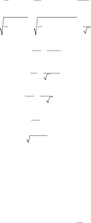
3.2.1 Half-wave rectifier
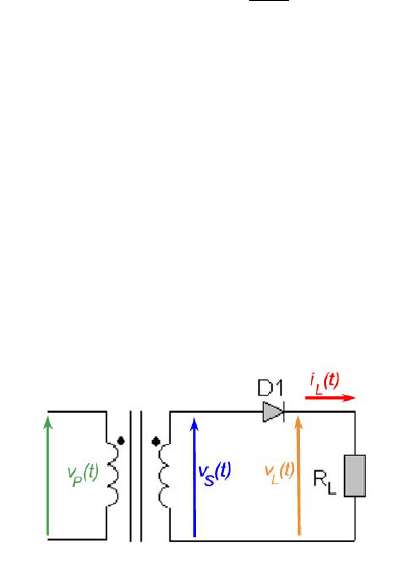
This is the simplest structure (Fig. 2). Only one diode is placed at the secondary of the transformer.
Fig. 2: Structure of the single-phase, single-way, half-wave rectifier
Figure 3 shows the waveforms of the voltage at the secondary and of the current in the load. Since the
load is a resistance, the voltage on the load is proportional to the current.
R. VISINTINI
136
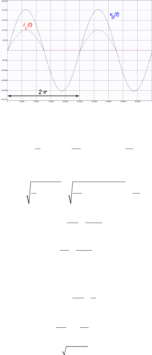
It is quite evident why this type of rectifier is called half-wave: the rectification process occurs
only during half-periods. It is also called single-way because the load current
i
L
(t) always circulates in
the secondary winding in the same direction.
Fig. 3: Waveforms of the single-phase, single-way, half-wave rectifier
Using the definitions reported in the previous section, we get the following results:
S
DC L S
00
11
()d sin( )d
2
T
V
VvttVtt
T
π
ϖ
ππ
== =
∫∫
. (17)
And, similarly, we can calculate the other parameters:
222
S
LL S
00
11
()d sin ( )d
22
T
V
Vvtt Vtt
T
π
ϖ
π
== =
∫∫
(18)
DC S
DC
LL
VV
I
R
R
π
==
⋅
(19)
S
L
LS
LL
2
V
V
II
RR
== =
⋅
. (20)
The current in the secondary of the transformer can flow only when the diode conducts and therefore
it is equal to the current in the load:
L
DC
2
V
FF
V
π
== (21)
2
2
14
0.405
FF
η
π
⎛⎞
===
⎜⎟
⎝⎠
(22)
2
11.21RF FF=−=. (23)
The poor performance of this rectifier is also confirmed by the utilization of the transformer. From
Eq. (14), we get
0.323TUF =
(or
0.286TUF =
according to some authors). (24)
RECTIFIERS
137
A direct current flows in the secondary of the transformer. This may result in saturation of the core,
which has to be sized accordingly.
From Fig. 3 it is clear that the inverse voltage seen by the diode in its blocking state is the
negative half-wave of v
S
(t). Similarly, the current that flows across the diode is the same as flows in
the load. For this topology, one has to choose diodes with
RRM S
VV> and
S
FRM
L
V
I
R
> . (25)
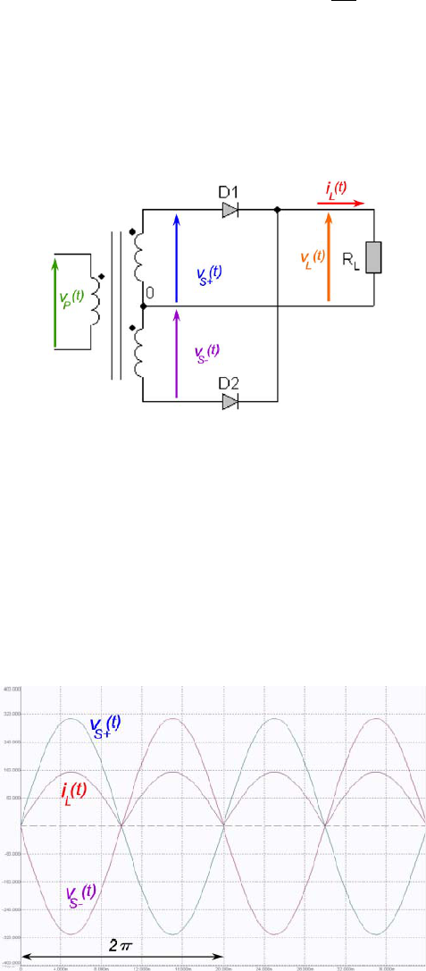
3.2.2 Full-wave rectifier — centre-tapped
In order to use both halves of the secondary AC voltage waveform, one can use two diodes and create
a return path for the current by adding a tap at the centre of the secondary winding (Fig. 4). This is the
so-called centre-tapped rectifier.
Fig. 4: Structure of the single-phase, single-way, full-wave rectifier
Diode D1 conducts during the positive half-wave of the voltage. Diode D2 conducts in the negative
half. The current always flows from the common point of the diodes, through the load and back to the
central tap of the transformer.
As shown in Fig. 5, the rectification occurs during the whole period of the voltage. This is a
full-wave rectifier.
It has to be noted that in this case as well the current flows in the same direction through the
two halves of the secondary winding. Therefore this is also a single-way structure.
Fig. 5: Waveforms of the single-phase, single-way, full-wave rectifier
R. VISINTINI
138
Using the definitions reported in the previous section and the symmetries, we get the following
results:
S
DC L S
00
2
12
()d sin( )d
2
T
V
VvttVtt
T
π
ϖ
ππ
⋅
== =
∫∫
(26)
222
S
LL S
00
11
()d sin ( )d
2
T
V
VvttVtt
T
π
ϖ
π
== =
∫∫
(27)
DC S
DC
LL
2VV
I
R
R
π
⋅
==
⋅
(28)
S
L
L
L
L
2
V
V
I
R
R
==
⋅
(29)
L
DC
1.11
22
V
FF
V
π
== =
⋅
(30)
2
1
0.81
FF
η
⎛⎞
==
⎜⎟
⎝⎠
(31)
2
1 0.483RF FF=−=. (32)
As it is a single-way topology, there is a direct current in both the secondary windings; this results in a
low TUF (compared to the bridge solutions, see next section).
0.671TUF = (or 0.572TUF = according to some authors). (33)
Even though this solution is much better than the previous one, there are some drawbacks. As can be
seen from Fig. 4, when a diode is conducting, the other, which is in the blocking state, sees the inverse
voltage of both windings of the secondary. The PIV of the diodes is higher. From the diode current
point of view, this topology is equivalent to two half-waves acting alternately. For this topology, one
has to choose diodes with
RRM S
2VV>⋅ and
S
FRM
L
V
I
R
> . (34)
3.2.3 Full-wave rectifier — bridge
The bridge structure is the best single-phase rectifier (Figs. 6 and 7). At the cost of two more diodes,
several advantages are obtained. This is a full-wave rectifier, but compared with the centre-tapped
solution it uses a simpler transformer, with a single secondary and no additional taps.
RECTIFIERS
139
Fig. 6: Structure of the single-phase, double-way, full-wave bridge rectifier
The rectification takes place by the conduction of couples of diodes. Diodes D1 and D4 are
conducting during the positive half-wave of the voltage. Diode D2 and D3 are conducting during the
negative half. This is a double-way topology. In each half-cycle the current flows in both directions in
the secondary winding but always in the same direction in the load. There is no DC component in the
winding and the core can be smaller than that for a centre-tapped rectifier with the same DC power
rating.
Since this is a full-wave topology, Eqs. (28) to (32) are still valid but the transformer utilization
factor is different. A sinusoidal current flows in both the primary and secondary windings, therefore
VA
P
= VA
S
. From the definition (14), using (26) and (28) and considering that i
S
(t) = i
L
(t) we get
DC DC
SS
0.813
22
VI
TUF
VI
⋅
==
⋅
. (35)
This is considerably higher than the TUF of the centre-tapped structure shown in (33).
Fig. 7: Waveforms of the single-phase, double-way, full-wave bridge rectifier
Looking at the PIV of the diodes, V
S
is the highest voltage seen by each diode in its blocking state.
Therefore the diodes must have
R. VISINTINI
140

RRM S
VV> and
S
FRM
L
V
I
R
> . (36)
Summing up: at the cost of two more diodes with reduced voltage ratings, we have a full-wave
rectifier, which, compared to the centre-tapped case of Section 3.2.2, for the same V
DC
and P
DC
requires a simpler and smaller transformer (23% oversized instead of 75%).
3.2.4 Summary
Table 1 (taken from Ref. [7]) summarizes the main performance parameters defined in Section 2 for
the three configurations presented above.
Table 1: Performance parameters for single-phase topologies
Half-wave Centre-tap Bridge
Peak repetitive reverse voltage V
RRM
π
V
DC
π
V
DC
π
/2 V
DC
r.m.s. input voltage per transformer leg V
Srms
2.22 V
DC
1.11 V
DC
1.11 V
DC
Diode average current I
F(AV)
I
DC
0.5 I
DC
0.5 I
DC
Diode peak repetitive forward current I
FRM
π
I
F(AV)
π
/2 I
F(AV)
π
/2 I
F(AV)
Diode r.m.s. current I
F(rms)
π
/2 I
DC
π
/4 I
DC
π
/4 I
DC
Form factor of diode current – I
F(rms)
/I
F(AV)
π
/2
π
/2
π
/2
Form factor – FF 1.57 1.11 1.11
Rectification ratio –
η
0.405 0.81 0.81
Ripple factor – RF 1.21 0.482 0.482
Transformer rating primary VA 2.69 P
DC
1.23 P
DC
1.23 P
DC
Transformer rating secondary VA 3.49 P
DC
1.75 P
DC
1.23 P
DC
Transformer utilization factor – TUF 0.324 0.671 0.813
Output ripple frequency f
R
(f
mains
= 50 Hz) f
mains
2 f
mains
2 f
mains
The values reported have been reorganized in terms of V
DC
(designer view): to achieve a given
DC output voltage one has to find the other design parameters going backwards from the output to the
AC mains.
Single-phase diode rectifiers, in the bridge configuration as well, require a high transformer VA
rating for a given DC output power. This type of rectifier is suitable for low power applications, up to
some kilowatts.
3.3 Multi-phase systems
3.3.1 Single-way structures (also known as star-connected rectifiers)
The use of single-way configurations—one diode per phase, each diode is conducting while the others
are blocked—becomes more convenient as the number of phases increases.
The circuit shown in Fig. 2 is single-phase. The circuit in Fig. 4 could be called bi-phase. By
extension, the circuit in Fig. 8 is m-phase.
RECTIFIERS
141
Fig. 8: m-phase, single-way rectifier
Figure 9 shows the waveforms of the phase voltages (in this example m = 3) and of the current
in the load. Each phase voltage has the same amplitude (V
S
) and the same frequency. There is a phase
displacement of 2
π
/m electrical radians between one voltage and the next. In one period there is a
specific number of peaks (usually called pulses), depending on the number of phases and on the
structure of the rectifier. The number of pulses in a period is indicated by p.
Fig. 9: Waveforms for the m-phase, single-way rectifier (m = 3)
For single-way topologies, the number of pulses is equal to the number of phases, i.e., p = m.
Each diode is conducting for 2
π
/m electrical radians and the rectified voltage can be expressed
by [8]
S
DC S
sin
cos( )
2
m
m
V
m
VtdtV
mm
π
π
π
ϖ
ππ
−
⎡
⎤
⎛⎞
⎜⎟
⎢
⎥
⎝⎠
⎢
⎥
==⋅
⋅
⎢
⎥
⎢
⎥
⎣
⎦
∫
, (37)
R. VISINTINI
142
2
2
S
LS
2
sin
1
cos ( ) 1
22
2
m
m
V
m
VtdtV
mm
π
π
π
ϖ
ππ
−
⎡
⎤
⋅
⎛⎞
⎜⎟
⎢
⎥
⎝⎠
⎢
⎥
==⋅⋅+
⋅⋅
⎢
⎥
⎢
⎥
⎣
⎦
∫
, (38)
L
DC
2
sin
1
1
2
2
sin
m
m
V
FF
V
m
m
π
π
π
π
⎡
⎤
⋅
⎛⎞
⎜⎟
⎢
⎥
⎝⎠
⎢
⎥
⋅+
⋅
⎢
⎥
⎢
⎥
⎣
⎦
==
⎛⎞
⎜⎟
⎝⎠
. (39)
From the definition of ripple factor (13), it is possible to write
1 0mFF RF→∞ ⇒ → ⇒ →
. (40)
This means that by increasing the number of phases in a multi-phase, single-way rectifier, the
result of the rectification is improved, i.e., the output voltage is smoother.
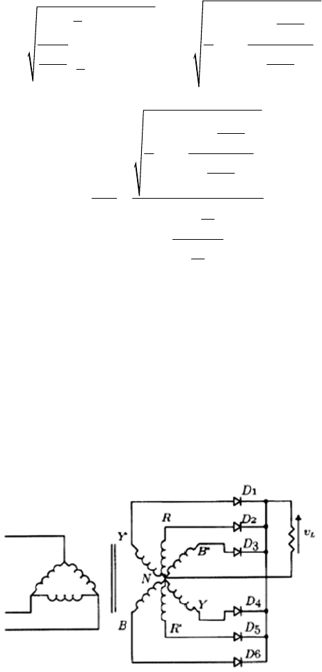
Connecting to a conventional three-phase mains distribution, it is possible to increase the
number of ‘phases’ by using transformers with m separated secondary coils. The secondary coils can
be connected in a great number of combinations, sometimes quite exotic, as can be found in the
literature (see for example Ref. [10]).
Fig. 10: Six-phase star-connected rectifier
The m-phase single-way connections are also known as star-connected rectifiers. Looking at the
configuration of the secondary windings of the rectifier presented in Fig. 10 (taken from Ref. [7]), the
origin of the name is quite clear.
The values for V
DC
and some other parameters have been calculated for m = 6, m = 12 and
m = 24 and are reported in Table 2.
As can be seen, passing from 6 to 12 pulses one gets a 3.5% improvement in the rectified
voltage while passing from 12 to 24 pulses this improvement is less than 1%. This is also shown by
the figures of the form factor for the three cases.
RECTIFIERS
143

Table 2: Performance parameter comparison for multi-phase, single-way topologies
m = 6 m = 12 m = 24
V
DC
/V
S
0.955 0.989 0.997
V
L
/V
S
0.956 0.989 0.997
Form factor (V
L
/V
DC
) 1.001 1.0001 1.0000
Ripple factor 0.042 0.0103 0.0026
Ripple frequency 6 f
mains
12 f
mains
24 f
mains
12 vs. 6 24 vs. 12
V
DC
vs. V
DC
1.035 1.009
V
L
vs. V
L
1.034 1.009
FF vs. FF 0.999 1
RF vs. RF 0.245 0.249
From Fig. 9 and Table 2 it is clear that the frequency of the ripple on the output is p times the
mains frequency f
mains
. This means that by increasing the number of phases (as stated before, in single-
way topologies, m = p), the ripple frequency increases and its amplitude decreases. This fact eases the
making of filters to reduce the ripple in the load.
The advantages of the reduced amplitude and increased frequency of the voltage ripple for the
12 and 24 pulses structures are counterbalanced by the growing complexity of the connections of the
transformer’s secondary windings. In practice, for single-way connections, the maximum number of
pulses is normally 12. As will be shown later, a higher number of pulses can be achieved by using
combinations of bridge structures.
In addition to the major complexity of the connections at the transformer’s secondary, in single-
way structures the current always flows in the same direction in each winding. There is a DC
component that may saturate the iron core and result in a poor utilization of the transformer, which has
to be correspondingly oversized. The best Transformer Utilization Factor (TUF) that can be achieved
with a single-way connection is TUF = 0.79 while with a bridge configuration it is possible to reach
higher values, up to TUF = 0.955 [8].
3.3.2 Six-pulse bridge configurations
In a bridge configuration, the number of pulses is twice the number of phases (p = 2m). It is possible
to obtain the same values for the rectified voltage and ripple factor using fewer phases, i.e., simpler
transformers with fewer windings and better utilization factor (fewer oversized transformers).
Starting from the basic 6-pulse structure shown in Fig. 11 it is possible to combine two bridges
in order to obtain 12 or more pulse rectifiers.
The PIV on the diodes in a bridge rectifier is half the PIV in an equivalent star rectifier: it is
possible to use components with a lower V
RRM
.
R. VISINTINI
144
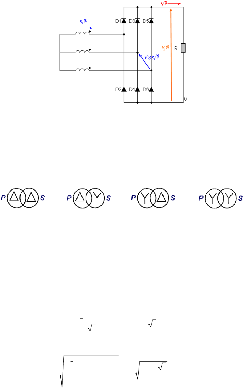
Fig. 11: Three-phase bridge rectifier
In Fig. 11 the secondary of the transformer is connected as a ‘Y’. Starting from a three-phase
mains distribution there are four possible combinations for the connections at the primary and the
secondary of the transformer: delta–delta, delta–Y, Y–delta and Y–Y (Fig. 12). They are not
equivalent. A delta primary requires three mains lines, without neutral, and avoids the so-called
excitation unbalance. With this connection, each winding is tied between two lines, the nonsinusoidal
exciting currents can be taken from the supply system so that there is a complete ampere-turn balance
and the excitation unbalance is avoided [10].
Fig. 12: Three-phase transformer connections (P = primary, S = secondary)
The Y secondary has some advantages compared to a delta one with the same turn ratio
between primary and secondary: the rectified voltage is
√3 times higher; the current in the windings is
the same as in the load; there is an easily accessible common zero-point in case one wants to get two
voltages with opposite sign (each side of the bridge acts as a single-way rectifier with m = 3).
The bridge structure is a double-way configuration; the secondary windings do not carry any
DC component and the currents are well balanced. The power ratings at primary and at secondary are
equal.
From the definitions presented in Section 2 and taking into account the symmetries given by the
presence of p = 6 pulses in the period, we get
2
3
DC S S S
3
633
3sin()d 1.654
2
VVttVV
π
π
ϖ
ππ
⋅
⋅
=⋅⋅==⋅
∫
(41)
2
3
22
LS S S
3
9393
sin ( )d 1.655
24
VVttV V
π
π
ϖ
ππ
⋅
⋅
=⋅ =⋅+=⋅
⋅
∫
. (42)
RECTIFIERS
145
As for the rectified voltage, the bridge acts as a single-way system with p = 2m pulses. By putting 2m
in Eqs. (37) and (38) instead of m, we obtain the same results.
Calculating the other performance parameters of Section 2, we get
1.009 0.998 0.042FF RF
η
== = . (43)
The r.m.s. current in each secondary winding is given by
S
S
L
3
23
64
V
I
R
π
π
⎛⎞
⋅
=⋅+
⎜⎟
⎜⎟
⎝⎠
, (44)
and the r.m.s. current through a diode is
S
D
L
3
13
64
V
I
R
π
π
⎛⎞
⋅
=⋅+
⎜⎟
⎜⎟
⎝⎠
. (45)
The TUF is calculated from definition (14) and is
0.955
DC
Srms Srms
P
TUF
VI
==
⋅
. (46)
3.3.3 Twelve-pulse bridge configurations
As shown in Table 2, a 12-pulse system performs much better in terms of rectification efficiency and
ripple content, both in amplitude and frequency, than a 6-pulse one. The three-phase bridge, along
with the possibility to use indifferently delta or Y secondary connections without affecting the
performance of the rectifier, makes it possible to build 12-pulse structures quite easily, avoiding
complex transformer configurations.
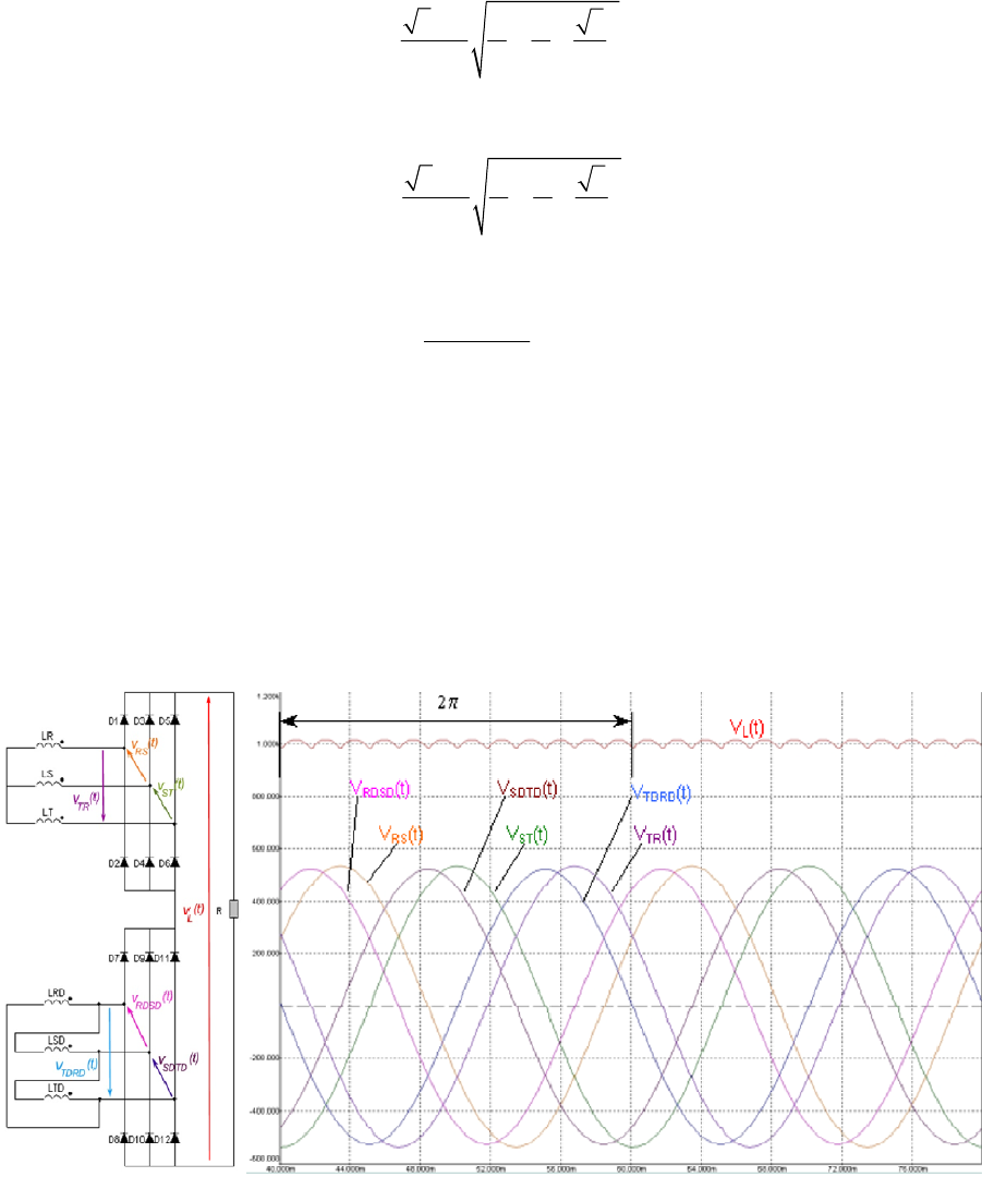
Figure 13 shows two 6-pulse bridges connected in series with the associated waveforms.
Fig. 13: Structure and voltage waveforms for two six-pulse bridges in series
R. VISINTINI
146
In order to achieve a proper 12-pulse operation, as shown in the plots on the left of Fig. 13, a
phase displacement of 30 degrees has to be introduced between the corresponding phase-to-phase
voltages of the two 6-pulse units. This is easily achieved by connecting one secondary as delta and the
other as Y.
The primary connection is normally delta to avoid excitation unbalance.
In order to obtain equal secondary voltages, the number of turns of the two secondary windings
must be in a ratio of 1:√3. Since √3 is an irrational number, the turn ratio of the two secondary
windings can only be approximated. Good ratios are 4:7 (1/1.75, i.e., +1% off) or 7:12 (1/1.71, i.e.,
–1% off) [10].
The values of the rectified voltage and of the other parameters are summarized in Table 3
(extracted from Ref. [7]).
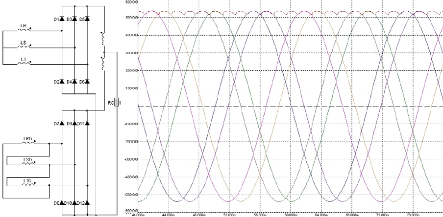
It is also possible to connect two 6-pulse bridges in parallel, as shown in Fig. 14 (the voltages
are the same of Fig. 13). In this case, it is necessary to insert an interphase reactance between the
bridges in order to adjust the instantaneous voltage difference.
Fig. 14: Structure and voltage waveforms for two six-pulse bridges in parallel
The load voltage, v
L
(t), is the average of the two output voltages from the bridges, v
B1
(t) and
v
B2
(t).
3.3.4 Summary
As reported also in Ref. [8], for multi-phase systems we can make the following observations:
–
The higher the number of pulses, the better the utilization of the rectifier, the lesser the ripple
amplitude and the higher the ripple frequency — this implies that filtering the ripple is easier.
Nevertheless, systems with a number of pulses higher than 12 (normally obtained by combining
two three-phase bridges) are not often used since their advantages are compensated by their
growing complexity.
–
Bridge structures are the most convenient in terms of TUF and PIV on diodes.
RECTIFIERS
147

– Single-way structures may become convenient for those applications where the output voltage
is so low that the voltage drop on diodes is no longer negligible. In a bridge there are two
diodes conducting and the voltage drop is double.
Table 3 (extracted from Ref. [7]) summarizes the main performance parameters for the three-
phase topologies described here. As in Table 1, the parameters are expressed in terms of DC output
(designer’s view). As already stated at the beginning of this section, in the literature and in practice
there are many other possible topologies, mainly based on particular arrangements of the transformer
windings or using more transformers connected via interphase reactors ([10], [11]).
Table 3: Performance parameters for some multi-phase topologies
3-ph star
(single-way)
6-ph star
(single-way)
6-pulse
bridge
12-pulse
series br.
12-pulse
parallel br.
Peak reverse voltage V
RRM
2.092 V
DC
2.092 V
DC
1.05 V
DC
0.524 V
DC
1.05 V
DC
r.m.s. input voltage V
Srms
0.855 V
DC
0.74 V
DC
0.428 V
DC
0.37 V
DC
0.715 V
DC
Diode average current I
F(AV)
0.333 I
DC
0.167 I
DC
0.333 I
DC
0.333 I
DC
0.167 I
DC
Diode forward current I
FRM
3.63 I
F(AV)
6.28 I
F(AV)
3.14 I
F(AV)
3.033 I
F(AV)
3.14 I
F(AV)
Diode r.m.s. current I
F(rms)
0.587 I
DC
0.409 I
DC
0.579 I
DC
0.576 I
DC
0.409 I
DC
Curr. form factor – I
F(rms)
/I
F(AV)
1.76 2.45 1.74 1.73 2.45
Form factor – FF 1.0165 1.0009 1.0009 1.00005 1.00005
Rectification ratio –
η
0.968 0.998 0.998 1.00 1.00
Ripple factor – RF 0.182 0.042 0.042 0.01 0.01
Transf. rating primary VA 1.23 P
DC
1.28 P
DC
1.05 P
DC
1.01 P
DC
1.01 P
DC
Transf. rating secondary VA 1.51 P
DC
1.81 P
DC
1.05 P
DC
1.05 P
DC
1.05 P
DC
Transf. Utilization Factor – TUF 0.73 0.647 0.952 0.971 0.971
Output ripple freq. f
R
3 f
mains
6 f
mains
6 f
mains
12 f
mains
12 f
mains
4 Three-phase controlled rectifiers
4.1 Introduction
In the first section we said that it is necessary to vary the output voltage of the rectifier. The structures
seen in Section 3 provide output voltages that are in a fixed ratio with the input AC voltages. The
diodes alone cannot satisfy our requirements. The next step is to substitute the diodes (all or only
some of them — creating the so-called full- or semi-controlled bridges) with thyristors.
The thyristor is a device whose transition from the blocking to the conducting state depends not
only on the polarity of the anode–cathode voltage (as for diodes, which are naturally commutating
devices) but is also controlled via the application of an adequate current pulse. Thyristors have three
terminals: the trigger pulse is applied to the gate while the anode–cathode voltage is positive. The
name thyristor derives from the Greek word thy-, meaning ‘switch’, and the suffix -istor, which
derives from transistor (trans-fer res-istor) to indicate that the device belongs to the semiconductor
family [12]. Sometimes it is called Silicon Controlled Rectifier (SCR) to distinguish it from similar
devices like the Gate Turn-Off thyristor (GTO) or the TRIode to control AC (Triac) or others, much
R. VISINTINI
148
less capable of handling high power, that are often used in the circuitry generating the trigger pulses
for the SCR. In the rest of this paper, thyristor means SCR.
In this section we still assume that we have ideal switches and purely resistive loads.
Here pages we shall only consider three-phase systems and those topologies that are more
commonly used to supply the load with variable voltage and, consequently, variable current.
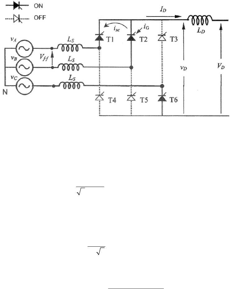
4.2 Three-phase fully controlled bridge
Figure 15 is equivalent to Fig. 11: here thyristors have replaced diodes.
Fig. 15: Three-phase fully controlled bridge rectifier
Similarly Fig. 16 shows the voltage waveforms with a delay angle
α
= 45 degrees.
Fig. 16: Waveforms of a three-phase fully controlled bridge rectifier (
α
= 45 deg)
The delay angle or firing angle, indicated as
α
, is defined as that angle in electrical radians or
electrical degrees comprised between the instant at which the thyristor would naturally switch on if it
were a diode and the instant at which the trigger pulse is applied and the thyristor starts to conduct
(assuming ideal devices with instantaneous turning on/off). In a bridge structure, two switches are
RECTIFIERS
149
conducting at the same time, i.e., two trigger pulses must be applied simultaneously to the couples of
thyristors that must conduct.
In order to calculate the rectified voltage as a function of the delay angle
α
, starting from
definition (1) and considering the symmetries, one should consider the two cases:
3
DC S S
DC DC0
63
() 3 sin( )d 3 cos()
23
() cos()
VVttV
VV
π
α
α
π
αϖ α
ππ
αα
+
=⋅⋅+=⋅⋅⋅
=⋅
∫
0
3
π
α
≤≤ (47)
2
3
DC S S
63
() 3 sin( )d 3 1 cos( )
23 3
VVttV
π
α
ππ
αϖ α
ππ
⎡
⎤
=⋅⋅+=⋅⋅⋅++
⎢
⎥
⎣
⎦
∫
2
33
ππ
α
⋅
<≤ . (48)
Equation (47) is valid when the condition of continuous conduction (i.e., the instantaneous voltage at
the DC terminals is at all times positive) is satisfied. For delay angles beyond 60 degrees the
instantaneous voltage at the DC terminals goes to zero (negative if the load has an inductive
component, as will be seen later) for a while and the current does not flow continuously anymore.
Figure 17 shows the load voltage waveforms at four different values of
α
.
Fig. 17: Waveforms of a three-phase fully controlled bridge rectifier at different values of
α
All performance parameters defined in Section 2 can be recalculated as function of
α
and there
are different equations depending on the type of conduction. They are reported in Appendix A.
4.3 Three-phase current regulator and diode rectifier
Thyristors are available with V
RRM
and V
DRM
higher than 6500 V (or more) and, at the same time, on-
state average currents exceeding 1200 A or even 3000 A (e.g. Powerex TBK0 or FT1500AU-240 or
EUPEC T2871N or T2563N). Nevertheless there are applications, like RF klystrons, requiring much
higher voltages, up to 100 kV [13] and [14].
Connecting thyristors in series, in order to handle the high voltage, introduces the additional
problem of their simultaneous firing: a very good equalization of the trigger pulses as well as of the
voltage drop on the stack must be guaranteed. If some thyristors of the stack are already conducting
while others are still turning on, the voltage on the components may reach destructive levels.
R. VISINTINI
150
For this reason it is preferable to use stacks of diodes, which are naturally commutating devices
that require no additional trigger. In order to keep the possibility of controlling the output voltage, a
pre-regulation with thyristors on the AC side is used, see Fig. 18.
Fig. 18: Three-phase current regualtor and diode bridge rectifier
The rectified output voltage as a function of the delay angle
α
is expressed by [15]
DC0
DC
DC0
DC
DC0
DC
( ) 1 cos( ) 0
23 3
( ) 3 sin( )
2332
55
( ) 3 1 cos( )
2626
V
V
V
V
V
V
ππ
αα α
πππ
αα α
ππ π
ααα
⎡⎤
=⋅+ + ≤≤
⎢⎥
⎣⎦
=⋅⋅ + <≤
⋅⋅
⎡⎤
=⋅⋅− − <≤
⎢⎥
⎣⎦
. (49)
For additional details, see the bibliography.
4.4 Three-phase uncontrolled or controlled bridge and linear regulator
Quite often there is a need to supply many low power loads (up to some kilowatts) or loads that
require a dynamics higher than that directly achievable with a plain line commutated rectifier, or there
is a need to supply loads having different characteristics with the same converter (this is the typical
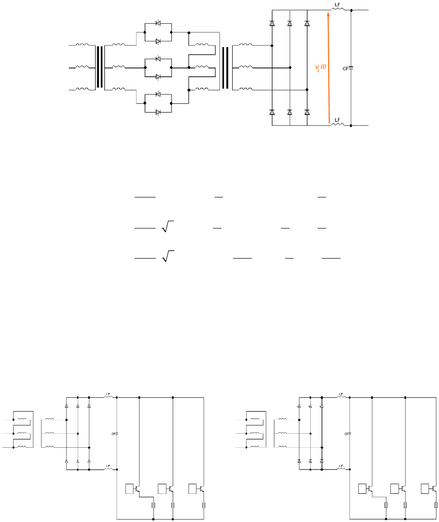
case of multi-purpose spare power supplies). Mixed structures can be applied, as shown in Fig. 19.
Fig. 19: Multi-channel linear transistor regulators with common diode rectifier (left) and fully controlled
rectifier with single linear transistor regulator (right)
A diode rectifier, followed by a passive filter for harmonic suppression (see next section),
provides the DC power for the channels hooked on the distribution rails. Each channel is a transistor
linear regulator (or PWM DC/DC module) that feeds a separate load. Two bridges, connected in series
RECTIFIERS
151
and using as return path the common point, provide positive and negative DC voltage to power 4-
quadrant (bipolar in voltage and current) transistor regulators.
The use of a thyristor bridge alone is not the best solution to supply loads that require variable
currents or loads with different characteristics (as in the case of spare power supplies), because at low
currents the delay angle is big and the ripple on the DC side is high. Neither is a diode rectifier really
suitable, since it provides a fixed DC voltage, and at low currents most of the output voltage drops on
the transistors of the regulator, increasing the losses. A fully controlled rectifier, followed by a filter
with a big reservoir capacitor and a series linear regulator, provides a high dynamics with high
efficiency and low ripple. Such power supplies are currently available on the market as standard
products.
5 The real converter: effects of the load and mains
5.1 Introduction
Until now, we have assumed we were working with ideal devices feeding pure resistive loads. The
real world is quite different.
First of all, the ripple on the DC side usually exceeds the tight specifications required for
particle accelerator applications. Even if 12-pulse structures are used, passive LC and often active
filters are needed to satisfy the ripple specifications for the DC.
The load usually has an inductive component. The time constant of the load,
τ
= L/R, can be
very high (hours in case of superconductive magnets), and, as we shall see, this is of great importance
for the operation of the converter.
The status of diodes and thyristors blocking or conducting changes in a finite, non-zero time
and they have a non-zero on-resistance that introduces losses during the conduction phase.
Last but not least, there is an inductance on the AC side of the rectifier (the inductance of the
secondary of the transformer and the stray inductance of the connecting lines).
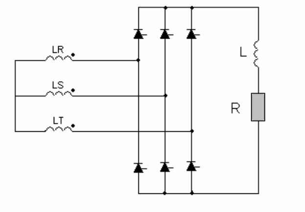
The real-world circuit, for example a 3-phases thyristor bridge rectifier, can be represented as in
Fig. 20.
Fig. 20: Six-pulse fully controlled bridge with inductive load
R. VISINTINI
152
5.2 DC side harmonics filtering
From Tables 1 and 3, it has been seen that the fundamental ripple frequency is given by
rmains
fpf=⋅
, (50)
where p is the number of pulses.
The ripple voltage at the output of the rectifier can be represented as an independent time-
varying voltage over/imposed on the average value of the rectified voltage (V
DC
). In order to reduce
the ripple amplitude, a passive LC filter is usually connected between the rectifier and the load. The
time-varying voltage can thus be interpreted as a composition of harmonics that are individually
weakened by the filter.
Assuming a p-pulse rectifier, the harmonics, whose number will be indicated with n, are whole
multiples of p. Since all currents and voltages are sinusoidal functions, by properly choosing the
origin of the reference system and using the symmetries, it is possible to represent the ripple voltage
as a Fourier series composed of cosine terms only whose amplitudes are described by [10]
nS
2
sin
2
cos 1
1
p
n
bV p nkpkN
p
n
p
π
π
π
+
⎡⎤
⎛⎞
⎢⎥
⎜⎟
⎡⎤
⎛⎞
⋅
⎝⎠
⎢⎥
=⋅ ⋅ ⋅− ≠ =⋅ ∈
⎢⎥
⎜⎟
⎢⎥
−
⎝⎠
⎣⎦
⎢⎥
⎢⎥
⎣⎦
, (51a)
that is,
nDC0
2
2
cos
1
n
bV
p
n
π
⎡
⎤
⎛⎞
⋅
=⋅ ⋅−
⎢
⎥
⎜⎟
−
⎝⎠
⎣
⎦
. (51b)
Equation 37 was used, replacing the number of phases ‘m’ with the number of pulses p. This result
shows that the amplitude of the harmonics is independent of the number of pulses and scales the
maximum rectified voltage V
DC0
with its harmonic number n.
It should be noted that Eqs. (51) are valid only for ideal devices (instantaneous commutation)
and delay angle
α
= 0. When taking into account real devices and phase control, the calculations
become complex and, therefore, only the fundamental harmonic is usually computed. This is normally
sufficient, since the higher harmonics are usually smaller and are weakened by the LC filter at a higher
ratio. For more details on the voltage and current ripples, from rectifiers, see the bibliography (e.g.,
Refs. [9] or [10]).
As already mentioned, passive LC filters are used to reduce the harmonics content on the output
of the rectifiers: “a combination of L and C produces a lower ripple with normal components values
than is possible with either L or C alone” [9]. The inductance smoothes the oscillations in the current
and the capacitance those in the voltage. The resonance frequency is given by
0
1
2
f
LC
π
=
⋅⋅
(52)
and it has to be chosen so as to satisfy the condition f
0
<< f
r
; furthermore, for a given f
0
, a degree of
freedom remains in the choice of L or C.
Some authors, e.g., Ref. [16], use economic criteria in choosing the proper compromise between
L and C. A purely technical approach consists in taking an inductance higher than the critical one. If
the load inductance is infinite, the current that flows through it is perfectly constant. As soon as the
RECTIFIERS
153
value of the inductance decreases, the attenuation of the current ripple also decreases. It was shown in
Section 4.2 — and in particular in Fig. 17 — that with a resistive (with a very small time constant)
load, at high delay angles (i.e., at low I
DC
), the instantaneous current in the load, i
L
(t), becomes zero,
entering the discontinuous mode. This should be avoided. The critical inductance is the minimum
inductance that guarantees a continuous current flow at the minimum I
DC
foreseen for the operation of
the rectifier with that particular load.
The critical inductance is calculated with the condition that the peak of the fundamental
harmonics of the current ripple through the filter inductance is equal to the minimum I
DC
in the load.
ripple _1 ripple _1
DCmin
r_1 r_1 DCmin
22
c
c
VV
IL
fL fI
ππ
= ⇒ =
⋅⋅ ⋅ ⋅⋅ ⋅
(53)
where V
ripple_1
is the amplitude of the fundamental harmonic of the ripple at frequency f
r_1
.
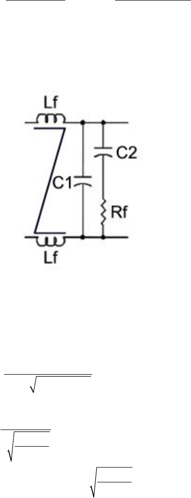
In order to avoid resonances, a damping resistor is normally added in the filter structure. A
typical scheme for a damped LC filter is given in Fig. 21.
Fig. 21: Damped LC passive filter
The resistance is chosen so as to limit the overshoot in the step response of the filter. From the
equation of the systems of the second order, with an overshoot equal to 1.5, the equations for this type
of filter are reported in (54) and an example of transfer function with f
0
= 25 Hz is shown in Fig. 22:
()
()
0
12
c12 12
12
12
1
2
4 or 5
2
0.2 0.4 .
f
LC C
LL C C C C
R
L
CC
L
R
CC
π
δ
δ
=
⋅⋅ ⋅ +
>=⋅ =⋅
=
+
= ⇒ =⋅
+
(54)
R. VISINTINI
154
1 10 100 1
.
10
3
30
25
20
15
10
5
0
5
10
15
Transfer Function Amplitude [dB]
3−
25
Fig. 22: Frequency response of a damped LC passive filter (f
0
= 25 Hz, damping factor
δ
= 0.2)
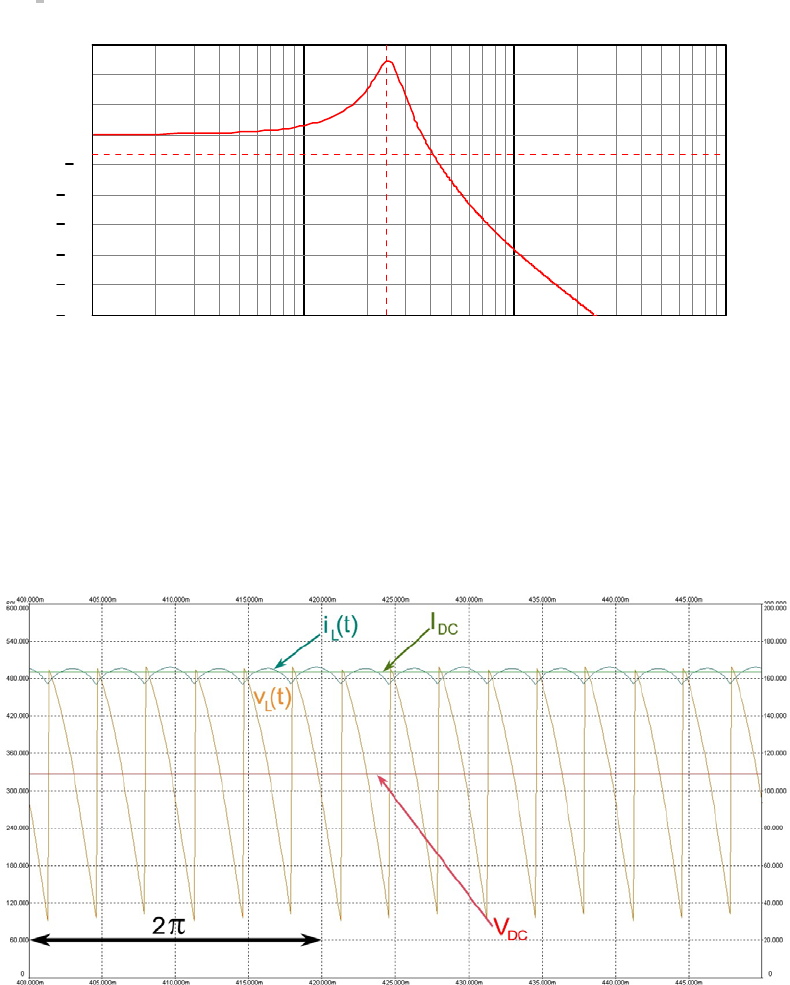
5.3 Effect of the inductance of the load
Owing to the presence of an inductive component in the load (Fig. 20)—including the inductance of
the passive filter—the current does not follow the voltage waveform but it is smoother and extends
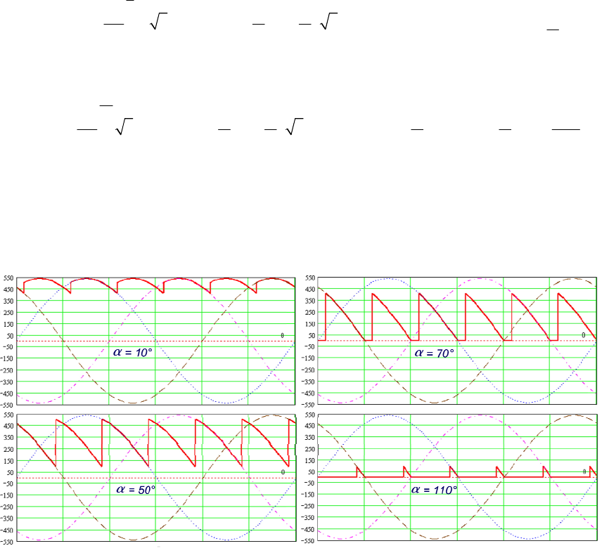
further depending upon the value of the inductance and of the firing angle (Fig. 23 shows as an
example the load voltage and current along with their average values for the circuit of Fig. 20 with
α
= 50°).
Fig. 23: Load voltage and current waveforms for a fully controlled bridge with inductive load and
with a delay angle
α
= 50° (left axis: voltage; right axis: current)
This fact keeps the thyristor in the conducting state for a longer time, even if the anode–cathode
voltage reverses and becomes negative (a thyristor, once it has been turned on, will remain on until the
anode current has been reduced to near zero, below the threshold value of the device).
For delay angles greater than 60 degrees, the output current remains continuous and positive
even if part of the load voltage waveform is negative. It should be noted that the load voltage is also
continuous, see Fig. 24, to be compared with the top-right plot in Fig. 17. The DC voltage, i.e., the
average of the rectified voltage (V
DC
), is also positive.
RECTIFIERS
155
Fig. 24: Output voltage and current waveforms for
α
= 70°; the load voltage is negative during
part of the period (its average is still positive) while the current is always positive (left axis:
voltages; right axis: current); two phase–phase voltages have also been plotted
The V
DC
becomes zero when the delay angle is 90 degrees and negative when the delay angle is
within 90 to 180 degrees. If the current is still positive (i.e., the inductance is sufficiently large), while
the V
DC
is negative, the power is fed back to the AC supply from the load. This operating mode is
called inverter or inverting mode. We shall come back to this topic later.
For a rectifier that operates in 1-quadrant mode (positive voltage and positive current), the
negative portion of the output voltage is a nuisance. The average value V
DC
decreases faster and the
delay angle range is in any case limited to 90 degrees. To prevent the output voltage from going
negative and, at the same time, let the current flow in the load even when the voltage is zero, a so-
called freewheeling diode is placed in parallel to the bridge (Fig. 25).
Fig. 25: Six-pulse fully controlled bridge with freewheeling diode and inductive load
When the output voltage becomes negative, the diode starts to conduct and the current of the
load flows through it. Another positive effect of the freewheeling diode is to reduce the voltage ripple
and the reactive power (the effects of the freewheeling diode on the bridge operations are particularly
well explained by J. Schaeffer and B.R. Pelly, see bibliography). The freewheeling diode is also an
effective protection against overvoltages when all firing pulses of the thyristors are stopped or the
main contactor on the primary of the transformer is opened (see Section 6.3).
R. VISINTINI
156
Figures 26 and 27 are useful to compare the effects of the freewheeling diode on the operation
of the rectifier for delay angles greater than 60 degrees. Two phase-to-phase voltages are also plotted.
Fig. 26: Output voltage and current waveforms of the circuit of Fig. 20 (
α
= 88°); the load voltage
is negative during part of the period (its average is almost zero) while the current is still positive
but with high ripple (left axis: voltages; right axis: current)
Fig. 27: Output voltage and current waveforms of the circuit of Fig. 25 (
α
= 88°); the effect of the
FW diode on the load voltage is evident (its average is also higher than that in Fig. 26; the scale of
the axis are the same in both plots) and the current is correspondingly higher and smoother (left
axis: voltages; right axis: current)
Figure 28 shows the voltage and current waveform for the circuit of Fig. 25 for a very large
delay angle (
α
= 100°).
RECTIFIERS
157
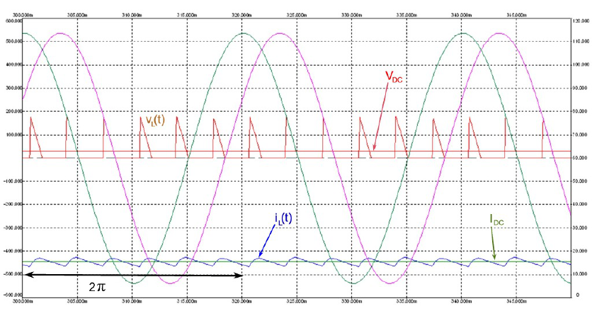
Fig. 28: Output voltage and current waveforms of the circuit of Fig. 26 (
α
= 100°); the load
current is still smooth even if the voltage is quite distorted (left axis: voltages; right axis: current)
Before closing the topic of the effects of the load inductance, I shall briefly describe the
inverting mode of operation. As was seen, with a highly inductive load and delay angles greater than
90 degrees and no freewheeling diode, the V
DC
is negative. If the I
DC
is still positive, power is flowing
from the load to the AC supply. The energy is transferred from the DC side to the AC one. This
operating mode can be used to extract energy from a large inductance (e.g., superconducting magnet)
when a rapid variation of the load current is needed.
In theory an inverter could work with delay angles up to 180 degrees. In practice this is not
possible. The overlapping angle
μ
(see Section 5.4), during which two phases are almost short-
circuited, reduces the angular operating range for the inverter. Moreover, the extinction angle has also
to be taken into consideration. It is defined as the minimum angle required by the thyristor to reach its
blocking state after commutation. It has to be
mains q
2
f
t
γ
π
>⋅⋅ ⋅ (55)
where f
mains
is the frequency of the AC mains and t
q
is the thyristor turn-off time.
The maximum delay angle is then given by:
max max
(usually, 150 )
απμγ α
=−− ≈
D
. (56)
If this condition is not satisfied, the commutation of the thyristor is not fully completed and
overcurrents may occur, resulting in the destruction of the device.
5.4 Thyristor commutation — effect of the AC input reactance
The commutation of real devices is not instantaneous. Turning on and off a diode or a thyristor takes a
finite time that may be as long as some tens or hundreds of microseconds (diodes turn off faster: some
tens of nanoseconds to some microseconds). Taking into consideration the thyristors only (we need to
control the DC level of the rectified voltage), turning off occurs when the anode current goes below
the so-called holding current I
h
.
R. VISINTINI
158
In addition to the finite turn off time, the inductance of the line and of the secondary of the
transformer plays an important role in rectifier operation. The commutation between the phases takes
a finite time, during which the two phases involved are almost shorted. This time (electrical angle) is
called commutating or overlapping time (angle), and it is usually indicated as
μ
.
Referring to Figs. 29 and 30 (taken from Ref. [7]), during the transition from phase B to phase
A, both thyristors T2 (which is turning off) and T1 (which is turning on) are conducting at the same
time. The current i
sc
is limited, in practice, by the impedance seen at the AC input of the rectifier, here
indicated as L
S
.
Fig. 29: Commutation of thyristors from one phase to another
The overlapping time
μ
depends both on the phase-to-phase r.m.s. voltage V
f-f
and on the
line/transformer secondary inductance (here indicated as L
S
). For a given direct current I
D
and the
corresponding delay angle
α
, it can be calculated from the following equation:
[]
f-f
D
S
cos( ) cos( )
2
V
I
L
αα
μ
ω
=⋅−+
⋅⋅
. (57)
The fact that during the commutation time two switches are conducting at the same time creates a sort
of short circuit and a reduction in the rectified voltage (v
D
) and in its average (V
D
). The reduction in
the DC voltage, indicated as ΔV
med
in Fig. 30, is given by
[]
f-f
med
3
cos( ) cos( )
2
V
V
αα
μ
π
⋅
Δ= ⋅ − +
⋅
(58)
or, referring to the average of the ideal rectified voltage [9, 10], it is possible to write
DC DC0
cos( ) cos( )
2
VV
αα
μ
++
=⋅
. (59)
RECTIFIERS
159
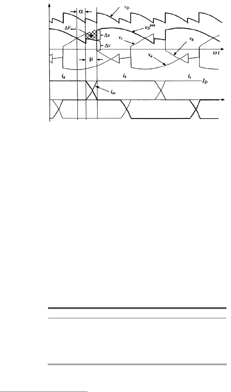
Fig. 30: Voltage and current waveforms showing the overlapping angle and its effect on the
rectified voltage (the load inductance L
D
is assumed to be large enough to consider the rectified
current I
D
to be constant)
As can be seen in Fig. 30, the waveform of the rectified voltage v
D
is additionally distorted
during the overlapping angle, worsening the output ripple of the rectifier.
5.5 Effect of the rectifier on the AC mains
5.5.1 Introduction
The switching action of the rectifying device inevitably results in a non-sinusoidal current being
drawn from the AC supply system. This non-sinusoidal current can be expressed as a fundamental
current at the mains frequency with harmonics superimposed on it. It can be demonstrated that to each
nth-order harmonic in the output voltage of the rectifier (n being an integer multiple of the number of
pulses p), there are two harmonics in the AC supply, whose orders are (n – 1) and (n + 1). In a first
approximation the amplitude of these harmonics, referred to the fundamental, decrease as 1/(n – 1)
and 1/(n + 1)
1
. Considering 3-phase rectifiers, Table 4 reports the first four harmonic components for a
6-pulse and a 12-pulse rectifier (e.g., a single and a double bridge—no matter if in series or parallel),
with a mains frequency of 50 Hz. Figure 31 shows the waveforms of the line current compared to its
fundamental harmonic component [17].
Table 4: First four harmonic components for 3-phase, 6- and 12-pulse rectifiers (f
mains
= 50 Hz)
6-pulse rectifier 12-pulse rectifier
Harmonic no. Frequency [Hz] Harmonic no. Frequency [Hz]
5 250 11 550
7 350 13 650
11 550 23 1150
13 650 25 1250
1
A more accurate calculation should take into consideration the overlap during commutation and the fact that the load
inductance is finite (this means that the current drawn from each phase during the conduction intervals is not constant).
R. VISINTINI
160
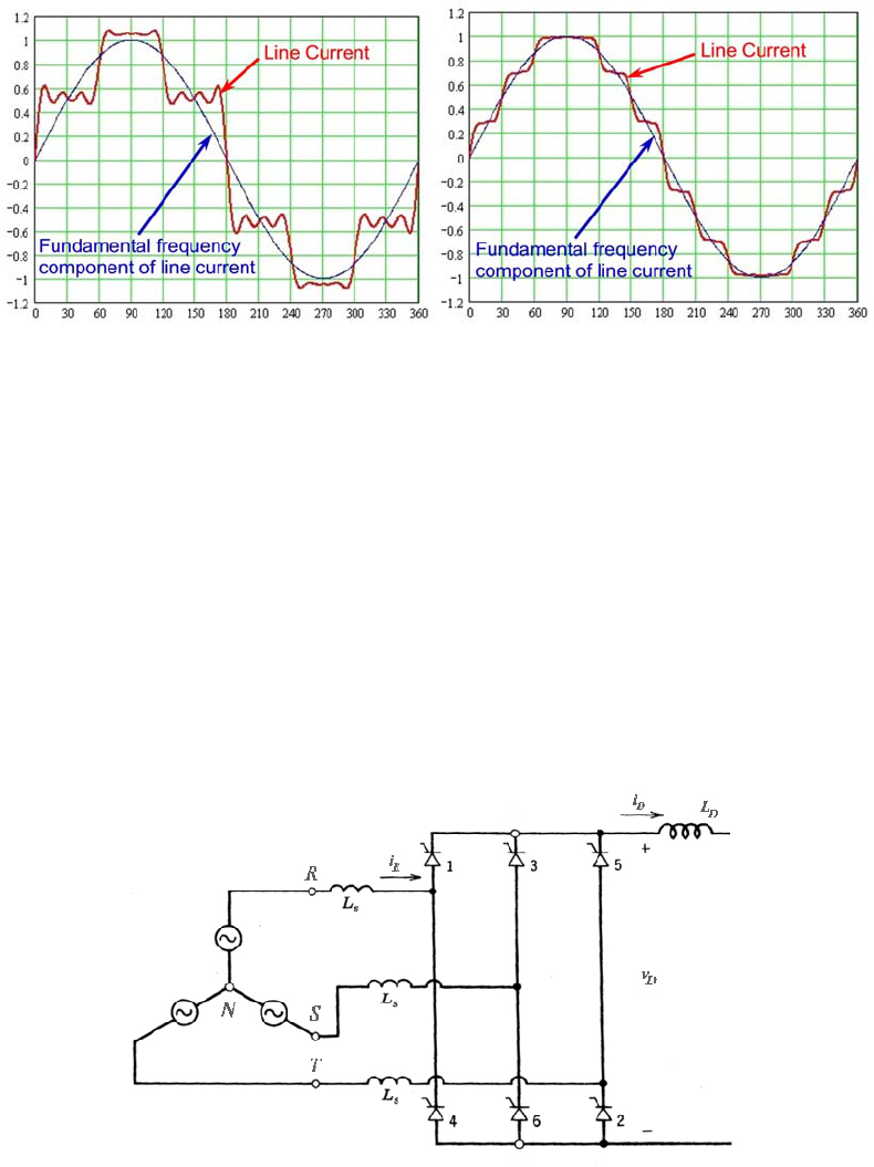
From Fig. 31 it is quite evident that a 12-pulse rectifier introduces less disturbance on the mains
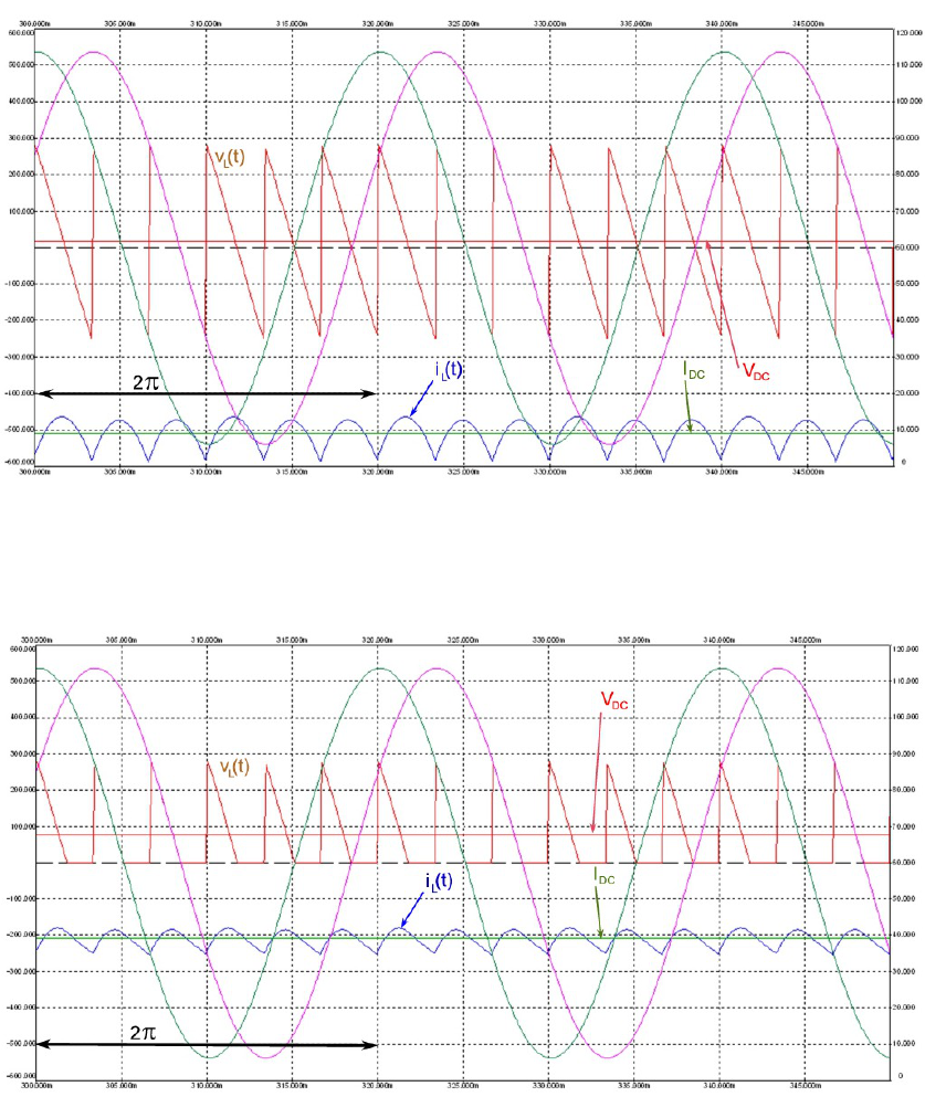
current than a 6-pulse one.
Fig. 31: Line current and fundamental harmonic component for the 6-pulse (left) and 12-pulse
(right) rectifier
In the following paragraphs I shall mention some of the effects on the network of the operation
of rectifiers. Refer to the bibliography (most of the mentioned books have dedicated chapters, but in
particular see Refs. [17] and [18]) for more details.
5.5.2 Power displacement factor and power factor [19]
Starting from the circuit of Fig. 32, let us consider the fundamental of the current only. We can define
as input displacement angle,
Φ
1
, the angular displacement between the fundamental components of the
AC line current and the associated line to neutral voltage (e.g., phase R, Figs. 27 and 28). The
Displacement Power Factor is defined as
)cos(
1
ΦDPF = . (60)
Fig. 32: Three-phase bridge. The load inductance L
D
is assumed to be large enough that the
rectified current i
D
is almost equal to the direct current I
D
.
Referring to the circuit of Fig. 32 and assuming a balanced steady-state operation, it is possible
to consider only one of the phases. The quantities for the other two phases will be identical except for
the ±120° displacement. The following plots show the waveforms of the line voltage v
R
and of the line
current i
R
for phase R in the ideal case (L
S
= 0, i.e., no overlapping) for two delay angles,
α
= 0°
(Fig. 33) and
α
= 30° (Fig. 34).
RECTIFIERS
161

Fig. 33: Voltage and current waveforms of phase R (i
R1
is the fundamental component of the line
current i
R
)
When
α
= 0° the waveforms of the line voltage and of the fundamental of the the line current
are in phase, i.e.,
Φ
1
=
α
= 0°. As soon as a positive delay angle is applied, i
R
(and hence i
R1
) start to
lag behind the v
R
by the delay angle
α.
Also in this case
Φ
1
=
α >
0
.
Fig. 34: Voltage and current waveforms of phase R (i
R1
is the fundamental component of the line
current i
R
)
The r.m.s. values of the Fourier components for the current waveforms are
R1 D
R1
Rn
23
2
1 1, 2, … .
II
I
Inkpk
n
π
⋅
=⋅
⋅
==⋅±=
(61)
The total r.m.s. value of the phase current is given by
22
RR1 Rn
1
k
II I
∞
=
=+
∑
. (62)
In this case the r.m.s. value of the phase current can be calculated to be
RD
2
3
II=⋅. (63)
The average power flowing through the rectifier is (V
R
and I
R1
are r.m.s. values)
RR1 1
cos( )PV I=⋅⋅ Φ. (64)
The apparent power is (I
R
is the r.m.s. value of the line current, which includes all harmonics)
RR
SV I=⋅. (65)
R. VISINTINI
162
The power factor is therefore defined as
R1 R1 R1
1
RRR
cos( ) cos( )
III
P
PF DPF
SI I I
α
==⋅Φ=⋅ =⋅ . (66)
Substituting (61) and (63) in (66) we get (for the circuit of Fig. 26)
3
cos( ) 0.955 cos( )PF
αα
π
=⋅ = ⋅ . (67)
This is an important result, showing that the power factor for a thyristor rectifier depends on the firing
angle
α.
Considering now the r.m.s. value of the distortion component in the line current,
22
Dis R R1
III=−, (68)
we define the total harmonic distortion as
22
RR1
Dis
R1 R1
II
I
THD
II
−
== . (69)
Up to now we have considered the ideal case of L
S
= 0, i.e., no overlapping. In the real world, L
S
> 0
and there is a positive angle
μ
> 0° to be added to the firing angle
α
. It is possible to approximate the
displacement power factor as:
cos( ) cos( )
2
DPF
αα
μ
++
≅
. (70)
The presence of the line inductance has, therefore, the effect of further reducing the power factor of
the rectifier.
5.5.3 Effects on the AC mains voltage [19]
As was seen in Section 5.4, during the commutation of the thyristors the two phases involved are
almost shorted through the line/transformer secondary reactance. This causes notches on the AC
voltage. It can be demonstrated that these notches have a maximum depth and width depending on the
delay angle
α
, the line/transformer secondary reactance L
S
, the phase-to-phase voltage V
f-f
, and the
average value of the rectified current I
D
.
f-f
SD
f-f
_2sin()
22
_ .
2sin()
Notch Depth V
f
LI
Notch Width
V
α
π
α
≅⋅⋅
⋅⋅⋅⋅ ⋅
≅
⋅⋅
(71)
The total harmonic distortion of the mains AC voltage can be calculated from the impedance of the
AC source (the line feeding the primary of the rectifier’s transformer) L
Sline
and the harmonics of the
converter’s input current. Using the notation of Eqs. 61 and 62, it is possible to write the following
equation:
()
2
Rn Sline
1
V
phase
2
k
In fL
THD
V
π
∞
=
⋅⋅⋅⋅ ⋅
=
∑
. (72)
RECTIFIERS
163
5.5.4 How to reduce the harmonics on the AC mains
According to Ref. [17], there are two types of solutions to mitigate the harmonics on the mains
current. They can be preventive or remedial ones. The former include the use of converters with a
high number of pulses (the total harmonic distortion in the line current for a 6-pulse and for a 12-pulse
rectifier are THD
6
= 28.45% and THD
12
= 9.14%) or with the proper choice of transformer connections
(delta-connected primary transformers are preferable). These make use of filters to damp specific
harmonic frequencies. The filters can be passive: a combination of capacitors and reactors — and
resistors for the damped type — tuned to the specific harmonic to be suppressed. There are also active
filters. They consist of a switched-mode power supply injecting into the line a current whose harmonic
spectrum is equal in amplitude and opposite in phase to that of the distorted harmonic current.
Harmonics are thus cancelled and the result is a non-distorted sinusoidal current.
5.5.5 Unity power factor rectifiers
In order to improve the harmonics content of the mains and, at the same time, to improve the power
factor of controlled rectifiers (which, as was seen, depends on the delay angle
α
), the so-called High
Power Factor or Unity Power Factor rectifiers are more and more studied (see, for example, Ref. [6])
and increasingly used. In principle they consist of a combination of conventional rectifier and PWM
techniques. Using an appropriate firing pattern for the PWM part, the waveform of the current drawn
from the AC line can be controlled to approximate a sinusoid in phase with the voltage waveform.
6 Protection and interlocks
6.1 Introduction
The topics of protection and interlock for power converters are covered by Steve Griffiths in another
paper of these proceedings [20]. In this section I just want to pinpoint some aspects of the problem,
and I shall briefly mention some precautions that should be adopted at the component level and for
whole converters. For more details, in addition to the above-mentioned paper, refer also to Refs. [16]
and [21].
6.2 Device protection
According to some, diodes are less fragile than thyristors. They do not include low-power gate circuits
and their simpler structure — a pn junction — makes them less sensitive than thyristors to
overcurrents, overvoltages and transients. Nonetheless they have to be protected and most of what is
mentioned in the following paragraphs about thyristor protection can be applied to diodes as well.
6.2.1 Overcurrent
The current rating of a device is the current which raises the temperature of the junction to its top limit
(normally around 125°C). An overcurrent will raise the temperature of the junction excessively and
cause malfunctions or the destruction of the device.
The simplest way to protect a thyristor is using adequate fuses. They must be fast acting fuses
preventing the rise to high arc voltages (less than 1.5 times the peak voltage in circuit). The I
2
t
parameter normally characterizes fuses: this value must be lower than the I
2
t that would damage the
thyristor (the semiconductor manufacturer usually indicates the maximum I
2
t for the protection fuses).
A more sophisticated method consists in monitoring the current through the device and
increasing the delay angle
α
as soon as the anode current exceeds a threshold. This system must be
able to bypass the normal control of the firing angle and must take into account the delay of the
protective action which, in fact, occurs only after the overcurrent is detected.
R. VISINTINI
164
Normal practice suggests choosing thyristors with peak current limits higher than the foreseen
operating conditions accepting a reasonable oversizing (between 30% and 50%).
6.2.2 Overvoltage
Withstanding the estimated reverse voltage for the application where it is used is one of the main
parameters for the design of the converter. If the thyristor is submitted to a reverse voltage greater
than its rated value, it will break down. Choosing oversized devices (V
RRM
30% or 50% higher than
that one expected) is also a good solution in this case.
Unlike diodes, thyristors have to be able to resist a forward voltage without turning on until the
gate trigger is applied. If an overvoltage exceeds the forward withstanding value, it turns the device
incorrectly on and can damage it. Again, an adequate oversizing of the V
DRM
(30% or 50% higher than
what is expected) solves the problem.
6.2.3 Transients
Voltage transients or voltage surges, i.e., an excessive slew rate of voltage (dv/dt) are another source
of overvoltages that may damage the thyristors. Transients may originate from sources that are either
internal or external to the device. The general approach to protect thyristors from voltage surges is to
quickly store the surge energy in a capacitor, and then to dissipate it slowly in a resistor.
Let us consider first transients internal to the circuit. Each thyristor commutation causes some
transient voltage peaks, in particular at turn off. Owing to the presence of an inductance (line,
transformer winding, etc.) in series during its conduction phase, a high peak reverse voltage is
generated when the thyristor is turned off. In order to mitigate this voltage surge, a RC combination,
called snubber circuit, is connected in parallel to each device.
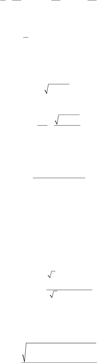
Figure 35 presents two versions of the snubber circuit. The principle is the same. Capacitor C1
suppresses the voltage surge dv/dt that appears when the thyristor Th goes into the blocking state.
Resistor R (R1) is used to damp possible oscillations in the LC circuit (L is the inductance of the AC
connection seen by the thyristor). The same resistance R (or, in the circuit on the right, R2) has to
limit the discharge current from the capacitor through the thyristor when it starts to conduct again. The
diode D in series with Rl is used to separate the action of the dv/dt protection resistor R1 (< R2) from
that of the discharge resistor R2.
Typical values for C are 0.1–1 μF and for R are 10–1000 Ω. More details on the dimensioning
of the snubber parameters are reported in the literature [8], [12] and in particular Refs. [9] and [22].
Fig. 35: Protecting thyristors from internal voltage surges: snubber circuits
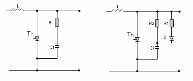
External transients come from the AC supply line. The main cause is the action of the power
converter’s main contactor; when it opens, it interrupts the magnetizing current at the primary of the
transformer. The energy stored in the secondary windings of the transformer is then dissipated through
RECTIFIERS
165
the thyristors and the load. When the contactor closes, a voltage overshoot may occur in the
oscillating circuit constituted by the inductance of the secondary windings and a capacitance, either
stray or physically present. Also in this case a RC combination is used. The capacitance must be able
to store the energy of the transformer. Sometimes the RC groups are connected directly between the
phases immediately before the rectifier. In order to decouple the capacitance from the inductance of
the connection, a bucket circuit is often preferred. In practice the RC group is connected to the line
through a diode rectifier (Fig. 36). Resistance R1 is the damping resistance, calculated from the
inductance of the line and of the transformer and the capacitance C. Resistance R2 is the discharge
resistor of the capacitor; it is sized in order to have a time constant of about 100 ms.
Fig. 36: Protecting thyristors from external voltage surges: bucket circuit
Some examples on how to calculate the bucket circuit parameters are presented in Refs. [8],
[16], [22], and [23].
6.3 Converter protection
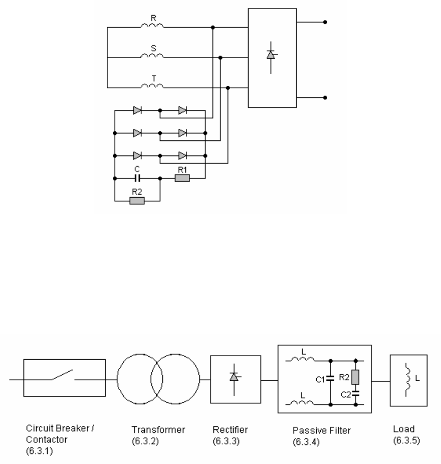
Referring to the unifilar schematic of Fig. 37, I shall quickly present some of the main aspects to be
considered in the protection of a complete converter.
Fig. 37: Diagram of the generic converter
R. VISINTINI
166
6.3.1 Circuit breaker and contactor
The circuit breaker’s duty is to disconnect the converter from the AC mains both under normal
operations (e.g., during maintenance) and in case of internal fault of the converter/load system. It has
to be chosen according to the short-circuit power rating of the AC line and has to switch off in case of
converter overload. Usually, for converters fed by a low-voltage line (380 V), there is a contactor
between the circuit breaker and the transformer for the normal On/Off operations.
Fig. 38: Circuit breaker with ‘soft start’ connection on the main contactor
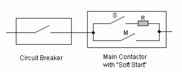
In order to limit the transformer’s magnetizing currents at the switch-on of the converter, a soft
start procedure is normally adopted (Fig. 38). The turn-on sequence is the following: command switch
on the first closes the secondary contactor S – the circuit breaker has already been closed — in order
to limit the inrush current through the resistor R; then, with S closed, after some hundred milliseconds,
the main contactor M is closed and, finally, S is opened. This procedure should include automatic
cross-checks on the status of S and M. If S is closed for too long while M is not, an interlock must be
triggered to open S and signal the presence of a problem in order to protect the limitation resistor.
6.3.2 Transformer
Assuming that the transformer has been correctly dimensioned to be used with a rectifier that
generates high harmonics in the secondary windings, the major risk for the transformer is high
temperature. Adequate cooling systems — oil, water, or air — must be provided and monitored.
Thermal sensors have to be mounted on the coils and connected to an interlock that switches off the
converter. The temperature of the coolant must also be monitored.
6.3.3 Rectifier structure
In Section 6.2 we discussed how to protect the devices (diodes or thyristors). Here I am considering
the rectifier structure. Adequate cooling is a very important issue. Thermal switches (connected to an
interlock) have to trip if the temperature of the heat-sinks is too high. Flow switches should monitor
the flow of water or of forced air used to cool the heat-sinks.
Normally, there is a passive filter cascaded to the rectifier, which, as presented in Section 5.2,
usually includes an inductance. To avoid overvoltages on the output of the rectifier structure when the
rectified current is suddenly interrupted (opening of the main switch, thyristors’ trigger pulses
disabled, etc.) a so-called ‘freewheeling diode’ is connected in anti-parallel to the rectifier structure.
6.3.4 Passive filter
A malfunction in the rectifier structure—for example a broken thyristor that does not turn on—
increases the ripple content in the rectified voltage. This leads to a great increase in the ripple current
through the capacitors of the passive filter. The capacitors have to be protected with properly sized
fuses or thermal contactors, or both. The magnetic components—the inductance—have to sustain the
whole rectified current (i.e., the DC component with the ripple current on it). Besides being
RECTIFIERS
167
adequately dimensioned in order to avoid saturation, they have to be properly cooled. Thermal
switches and—if water or forced air is used—flow switches have to be planned for.
6.3.5 Load
Protections for the load are also included in the converter’s structure. If the load has a high inductive
component, a freewheeling diode is normally connected at the output of the converter in anti-parallel
to the load. The freewheeling diode has to be able to withstand the peak load current.
It is not good practice to let float the load and the output of the power supply. In case of fault or
accident, if the power supply or the load goes to earth potential, very high currents could be generated.
Normally, the low side of the converter output is connected to earth through a resistor and the current
that flows through it is monitored. If this earth current exceeds a certain threshold, this may indicate a
problem of the load or of the converter.
The load itself has to be adequately cooled and there should exist individual protections (e.g., if
the load is a string of magnets) against over temperature and other parameters (e.g., the flow of
cooling water or the quench detection in superconducting magnets) that act as external interlocks,
switching off the associated power supply.
6.3.6 Additional protections/interlocks
Under this category, one could include interlocks related to a malfunction of the converter (e.g., one
or more missing phases in the AC mains—including voltage sags—or error signal on the output
current reading device, absence of remote control, etc.), or those related to the safety of the personnel,
like door switches on the cabinet that contains the converter, emergency turnoff push buttons, etc.
7 Example of dimensioning
7.1 Introduction
In this section I present the dimensioning, based on Refs. [24] and [25], of a DC magnet power supply
that has been operating since 1993 at the Elettra Synchrotron Light Laboratory. The calculations have
been reorganized in a Mathcad
©
worksheet. The names of the constants and of the variables are those
used in the calculations. The Mathcad
©
notation is used in the following paragraphs.
7.2 System requirements and technical specifications
The load consists of two quadrupole magnets connected in series. Its characteristics are
Load inductance: L
m
= 27 mH
Load resistance (including cables) : R
m
= 105 mΩ
Maximum DC output voltage (incl. safety margin): V
DC
= 40 V
Maximum output current (incl. 10% safety margin): I
DC
= 385 A
Minimum output current (10% of nominal one): I
DCmin
= 35 A
Power supply output power: P
DC
= V
DC
I
DC
= 15.4 kW
For test purposes, the power supply has to operate at full current on a load 25% of nominal.
Maximum output current ripple (ΔI/I
DC
): γ
ripple
= 2 × 10
-5
A step-down transformer provides the AC voltage. The characteristics of the transformer are as
follows:
R. VISINTINI
168
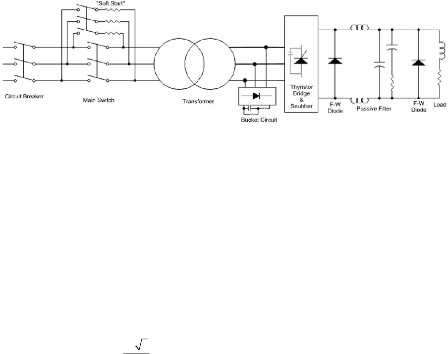
Transformer ratio: 20/0.4 kV
Nominal mains voltage: V
mains_rms
= 380 V
Maximum mains voltage variation: ΔV
mains
= 10%
Short-circuit power of the transformer: P
SC_trafo
= 1.6 MVA
Short-circuit voltage of the transformer: V
SC_trafo
= 7.5%
Mains frequency: f
mains
= 50 Hz
7.3 Dimensioning of the components
The general scheme of the power supply is shown in Fig. 39. In the following paragraphs the main
components of the power supply will be calculated by means of the definitions and formulas reported
in the previous sections with some additional details when needed.
Fig. 39: Summary of protections and interlocks on a converter
7.3.1 Transformer
In order to dimension the transformer, the no-load DC voltage has to be obtained. This voltage
includes all losses.
Voltage drop on thyristors (2 switches: it is a bridge structure): V
Th
= 1.5 V
Voltage drop on filter inductance and inner connections: V
L_conn
= 0.5 V
Voltage drop on transformer:
trafo
:3%VΔ=
Voltage drop due to initial end stop delay angle:
end_stop
:3%VΔ=
The rectification structure is a fully controlled 3-phase bridge. The rectification ratio between the
r.m.s. secondary interphase voltage and the average rectified voltage is
V_Br
32
:
r
π
⋅
=
V_Br
1/35r = .
The required no-load voltage is given by
()
()
()
()
DC0 DC Th L_conn trafo end_stop mains
:2 1 1 1VVVV V V V=++ ⋅+Δ⋅+Δ ⋅+Δ
DC0
50 764 VV.= .
The r.m.s. secondary phase-phase voltage is
RECTIFIERS
169
DC0
S
V_Br
:
V
V
r
=
S
37.6 VV = .
From the ratio between the average rectified current and the r.m.s. value of the phase current, it is
possible to calculate the r.m.s. secondary phase current:
I_Br
2
:
3
r =
I_Br
0.816r =
SDCI_Br
:IIr=⋅
S
314.4 AI = .
The dimensioning power of the transformer is (for a bridge rectifier the power at the secondary is
equal to the power at the primary)
Tr S S
:3PVI=⋅⋅
Tr
20.467 kVAP =
.
The r.m.s. primary phase current (including a 5% safety margin for the magnetizing current and other
losses) is
Tr
P
mains_rms
:1.05
3
P
I
V
=⋅
⋅
P
32.7 AI = .
Since the transformer has to be installed inside the cabinet containing the power supply, a
demineralized-water-cooled type is chosen.
7.3.2 Circuit breaker and main contactor
The short-circuit current of the upstream transformer (the one that feeds the mains line) defines the
breaking capacity of the circuit breaker for the converter:
PC_trafo
SC
mains_rms SC_trafo
:
3
P
I
VV
=
⋅⋅
SC
32.413 kAI = .
The circuit breaker has to have a breaking capacity higher than
I
SC
= 32.4 kA and its size has to
be greater than
I
P
= 32.7 A. A commercially available size could be I
CB
= 35 A. This is also the size of
the main contactor.
When a transformer is initially connected to the mains, there may be a substantial surge of
current through the primary winding (inrush current). This current surge may be quite high if the core
saturates (this is possible since transformers’ cores are usually dimensioned to sustain the magnetic
flux during normal operations) and should be limited. After a few periods the current surge is reduced
to the normal value of the magnetizing current. The limitation of the current surge is achieved by
using an additional contactor in parallel to the main one that connects the primary of the transformer
to the mains line through resistors.
The secondary contactor with its thermal protection and the resistors has to sustain the
magnetizing current of the transformer:
μ P
:5%II=⋅
μ
1.6 AI = .
The chosen resistors (and their power ratings) are
μ
:4.7 R =Ω
2
μμ
12.5 WRI⋅=
.
R. VISINTINI
170
Since the price difference is not too high, for safety reasons let us take 50 W resistors. The
commercially available one, for example, a 5 A secondary contactor should feature a thermal relay set
to
μ
50 W/R 3 A= .
7.3.3 Bridge thyristors, snubber and bucket circuits, freewheeling diodes
The choice of the thyristors depends on the average and r.m.s. currents, on the peak voltages (forward
and reverse) and on the peak current it may experience in case of short circuit of the load. The currents
and peak voltages are (see Table 3)
DC
Th_avg
:=
3
I
I
Th_rms DC
:= 0.579II⋅
Th_Peak DC0
:=1.05VV⋅ .
Therefore the
I
F(AV)
and I
F(rms)
and V
RRM
of the thyristor have to be higher than
Th_avg
= 128 AI
Th_rms
= 222.9 AI
Th_Peak
= 53.3 VV .
The peak current in the thyristors depends also on the short-circuit voltage of the transformer. This
short-circuit voltage can be assumed to be
V
Tr_SC
= 6%. Additionally, the current flow in the load
depends also on the impedance of the transformer’s secondary and of the connection to the thyristors.
Since
X
Tr
= ω L
Tr
the reactive component and R
Tr
the resistive component, according to
Ref. [10], Chapter 11, from which Fig. 40 has been taken, the peak current depends on the crest
transient factor, which is a function of the ratio
X
Tr
/R
Tr
. From Fig. 40, assuming X
Tr
/R
Tr
= 6, the crest
factor is
f
crest
= 1.6.
Fig. 40: Transient factors
RECTIFIERS
171
The peak of the short circuit current is:
S
Th_SC_Peak crest
Tr_SC
:= 2
I
If
V
⋅⋅
Th_SC_Peak
= 11.9 kAI .
Assuming 10 ms (half-period) time span before the intervention of the protections, the resulting
I
2
t is
()
2
10
2
Th_SC_Peak mains
0
:sin2d(t)
ms
It I f t
π
⎡⎤
=⋅⋅⋅
⎣⎦
∫
52
12 7.027 10 A st =× .
The thyristors have to have a I
2
t characteristic higher than that calculated above.
To calculate the snubber network, R
sn
and C
sn
, to be placed individually on each thyristor to
suppress the reverse recovery voltage, it is necessary to know the stored charge in the thyristor. The
stored charge depends on the rate of commutation, which is related to the reactance of the secondary
of the transformer. The leakage inductance at the secondary of the transformer can be calculated as
follows:
S
Tr_S Tr_SC
mains S
:
2
V
LV
fI
π
=⋅
⋅⋅ ⋅
Tr_S
22.8 μHL = .
The peak secondary voltage and the rate of commutation, di/dt, are given by
S_peak S
:2VV=
S_peak
53.16 VV =
S_peak
6
Tr_S
A
1.2 10
2s
V
L
=×
⋅
.
For the chosen thyristor, at the on-state current of
DC
385 A,I = the recovered charge can be as high
as
Q
Tr
= 130 μC .
The capacitor and the resistor can be calculated as follows [22]:
Tr
sn_t
S_peak
:
Q
C
V
=
sn_t
:2.45 μFC = standard value:
sn
:2.7 μFC = .
To limit the overvoltage to 15%, the damping factor should be ξ = 0.5 and, consequently, the damping
resistance has to be
Tr_S
sn_t
sn
2
:2ξ
L
R
C
⋅
=⋅⋅
sn_t
4.11 ΩR = standard value:
sn
4.3 ΩR = .
We use a bucket circuit to protect the bridge from overvoltages generated by the opening of the main
switch while the thyristors are conducting. From Ref. [8] or Ref. [9], the capacitor and the resistance
are calculated as follows. The magnetizing current of the transformer transferred to the secondary is
μ_S S
:5%II=⋅
μ_S
15.7 AI = .
R. VISINTINI
172
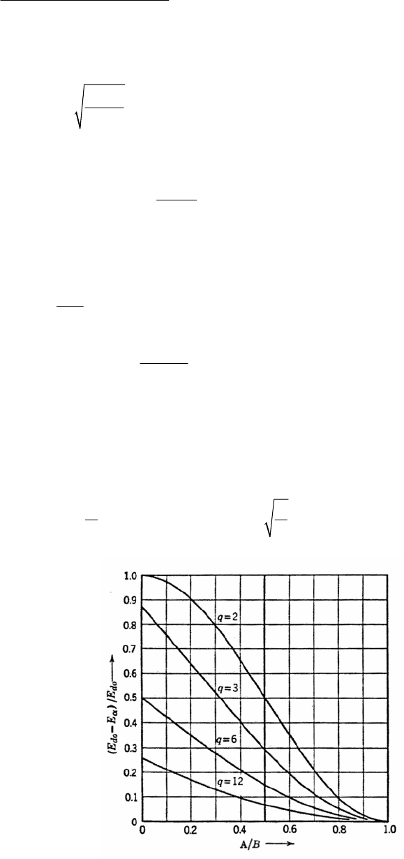
Assuming an overvoltage k
V
= 1.55 (between the overvoltage and the peak voltage at the secondary)
we have
()
μ_S
BCt
2
mains v S_peak
:
21
I
C
fkV
π
=
⋅⋅ ⋅ −⋅
BCt
: 671.038 μFC = standard value:
BC
:680 μFC = .
Accepting a 15% overvoltage, ξ = 0.5, the damping resistance is
Tr_S
BCt
CB
2
:2ξ
L
R
C
=⋅⋅
BCt
0.259 ΩR = standard value:
BC
0.27 ΩR = .
The diode bridge of the bucket circuit has to be chosen in order to sustain the peak current, i.e.,
S_peak
BC_peak
BC
:
V
I
R
=
BC_peak
: 196.9 AI = .
In parallel to the capacitor there is a discharging resistor. It can be chosen assuming a time constant
τ
BC
= 0.25 s:
BC
BC_disc_t
BC
τ
:R
C
=
BC_disc_t
:368 R =Ω standard value:
BC_disc
:360 R =Ω
maximum dissipated power:
2
S_peak
BC_disk
8 W
V
R
= .
In parallel to the thyristor bridge and the load, we install freewheeling diodes. Let us calculate their
parameters. According to Ref. [10], Chapter 13, the average and r.m.s. currents carried by the
freewheeling diodes are a function of the ratio A/B between the real output voltage and the maximum
possible rectified voltage. Neglecting the commutation angle μ, and referring to Fig. 41 (taken from
Ref. [10]), it is possible to write:
FW_avg DC
:
A
II
B
=⋅
FW_avg DC
:
A
II
B
=⋅
dd0α
E
EE=−.
Fig. 41: Chart for calculating the freewheeling diode currents
RECTIFIERS
173
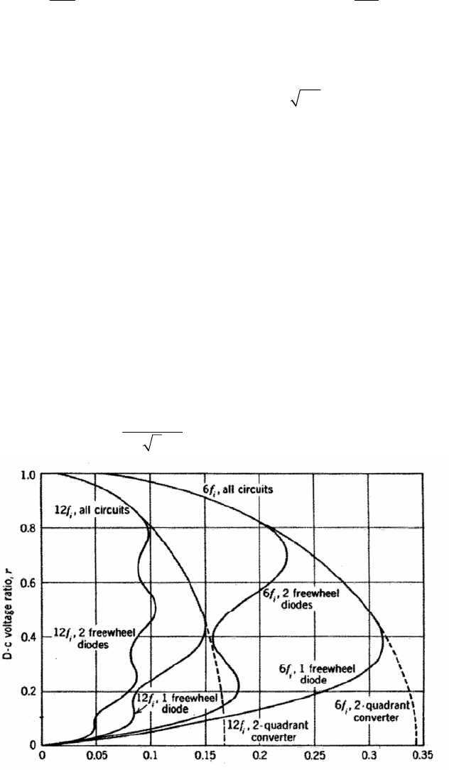
It is possible to see that the worst case is when the load resistance is 25% of the nominal one, where
we have
DC
d
:
4
V
E =
d
:10 VE =
d0 DCO
:EV=
d
d0
0.197
E
E
= .
From the curve for q = 6 (q is the number of pulses), we get A/B = 0.4 and therefore the maximum
average and r.m.s. currents in the freewheeling diodes are
FW_avg DC
:0.4II=⋅
FW_avg
154 AI =
FW_rms DC
:0.4II=⋅
FW_rms
243.5 AI = .
Thyristors and diodes have to be mounted on heat-sinks properly dimensioned to dissipate the heat
and keep their junction temperature <125°.
7.3.4 Passive filter
Using a 3-phase bridge, the frequency of the first harmonic of the ripple is
ripple_1 mains
:6
f
f=⋅
ripple_1
300 Hzf = .
In order to dimension the filter, let us consider the first harmonic only. A filter with a good attenuation
at that frequency will provide an even better attenuation for the higher frequencies. According to
Ref. [11] [see also Fig. 42)], the maximum ripple voltage is given by
ripple_1_pk S
: 0.33 1.35VV=⋅⋅
ripple_1_pk
16.7 VV = .
ripple_1_pk
ripple_1_rms
:
2
V
V =
ripple_1_rms
11.8 VV = .
Fig. 42: Peak amplitude of first harmonic (x-axis) vs. DC voltage ratio
The nominal load impedance as a function of the frequency [ω(f) = 2
π
f] is
() ()
mm m
: ω
Z
fRifL=+⋅ ⋅.
R. VISINTINI
174
At the fundamental ripple frequency, the amplitude of the ripple current in the load is
()
ripple_1_pk
ripple_1_pk
m ripple_1
:
V
I
Zf
=
ripple_1_pk
0.329 AI =
ripple_1_pk
4
DC
8.5 10
I
I
−
=× .
The filter has to provide an attenuation of
ripple
filter
ripple_1_pk
DC
γ
γ :
I
I
=
filter
γ
0.023= .
This corresponds to an attenuation of –32.8 dB.
According to Ref. [8], the resonance frequency of the passive LC filter, f
0
, is given by
0 ripple_1 filter
: γff=
0
45 9 Hzf.=
.
The calculated frequency is too close to the mains frequency, we can choose f
0f
= 30 Hz.
The minimum inductance value is calculated assuming continuous conduction at the minimum
rectified current. As shown in formula (5.4), the critical inductance is given by
ripple_1_pk
c
ripple_1 DCmin
:
2
V
L
fI
π
=
⋅⋅ ⋅
c
230.8 μHL = .
Let us take L
f
= 250 mH. The r.m.s. current of first ripple harmonic is
ripple_1_rms
ripple_1_rms
ripple_1 f
:
2
V
I
f
L
π
=
⋅⋅ ⋅
ripple_1_rms
25.1 AI = .
Let us assume a 25% margin on the current in order to include all ripple harmonics:
ripple_rms ripple_1_rms
:1.25II=⋅
ripple_rms
31.41 AI = .
From the cut-off frequency equation, it is possible to calculate the value of the capacitor:
0f
ff_t
1
2
f
LC
π
=
⋅⋅ ⋅
f_t
22
f0f
1
:
4
C
Lf
π
=
⋅⋅ ⋅
f_t
112.6 mFC = .
By taking a standard value for the capacitor we slightly change the cut-off frequency:
f
: 150 mFC =
ff
1
26 Hz
2 LC
π
=
⋅⋅ ⋅
.
It is better to insert a damping resistor in order to limit the overvoltage at the cut-off frequency. The
structure of the filter is shown in Fig. 43 (Section 5.2):
RECTIFIERS
175
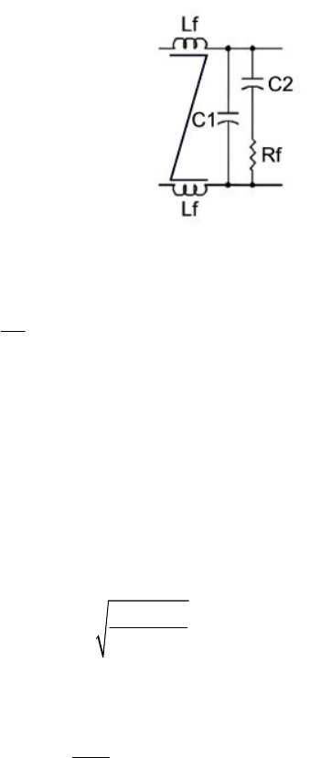
Fig. 43: Passive filter structure
f
1
:
5
C
C =
21
:4CC=⋅
1
30 mFC =
2
120 mFC =
considering a 25% margin on the maximum voltage on the capacitors, their voltage rating (including a
10% fluctuation on the mains) has to be higher than
S_peak
1.1 1.25 73.1 VV⋅⋅ = .
The nearest commercial size is 100 V.
To calculate the damping resistor, we can impose a critical damping (no overshoot) of the step
response, that is
δ
f
= 1.
()
f
f_t f
12
:2δ
L
R
CC
=⋅
+
f_t
81.6 mR =Ω.
Using five standard resistors in parallel,
f
0.43
:
5
R =Ω
f
86 mR =Ω
.
Calculating the impedances of the filter and of the load at the first harmonic frequency of the ripple, it
is reasonable to assume that most of the ripple current flows through the two parallel capacitor
branches. Considering a 25% margin to also take into account the higher-order harmonics, the currents
in C
1
and (C
2
+ R
f
) are
ripple_rms_1
26.1 AI =
ripple_rms_2
5.4 AI = .
The power dissipated by R
f
is
2
Rf_t f ripple_rms_2
:PRI=
Rf_t
2.5 WP = .
The peak currents in the resistor at turn-on or in case of accidental oscillation of the bridge regulation
are much higher than 5.4 A
rms
. It is better to take 25 W resistors.
At this stage it is possible to calculate the transfer function of the filter F
f
(f) = (V
out
/V
in
) and plot its
Bode diagram (Figs. 44 and 45).
R. VISINTINI
176
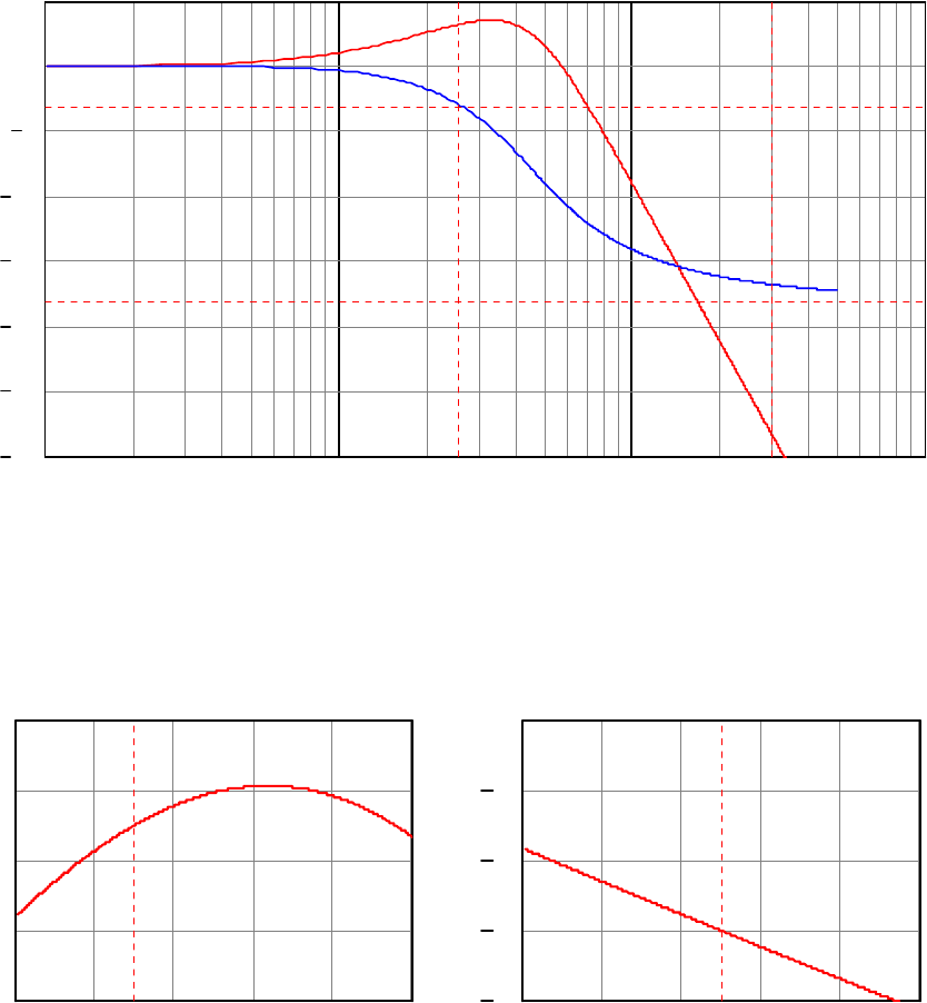
1 10 100 1
.
10
3
30
25
20
15
10
5
0
5
Amplitude[dB] & Phase [Deg/10]
3−
18−
30026
Fig. 44: Bode diagram of the LC passive filter (critical damping)
Zooming in the two bands 20–40 Hz and 64–74 Hz, it is possible to see that the actual resonance peak
is at ~32 Hz and the
3− dB frequency is ~70 Hz. This is the effect of inserting the damping resistor.
20 24 28 32 36 40
2
2.5
3
3.5
4
Amplitude[dB]
26
65 67 69 71 73 75
4
3
2
1
0
Amplitude [dB]
70
Fig. 45: Zoomed areas of the Bode diagram of Fig. 44
The filter attenuation at the fundamental ripple frequency is –28 dB. This is far from the original
requirement of –32.8 dB. To stay within the ripple specifications, we should change some parameters
of the filter or start to consider adding an active filter at the output of the power supply in order to
attenuate the remaining ripple.
As an example, let us accept a 50% overvoltage in the step response of the filter. This means
that the damping factor is
δ
f0
= 0.2 and the damping resistor is R
f0
= 0.2 Ω. The Bode plot is reported
in Fig. 46 and the attenuation at 300 Hz is –31.6 dB.
RECTIFIERS
177
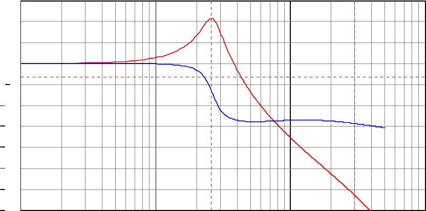
1 10 100 1
.
10
3
35
30
25
20
15
10
5
0
5
10
15
Amplitude[dB] & Phase [Deg/10]
3−
30026
Fig. 46: Bode diagram of the LC passive filter (non-critical damping)
7.3.5 Current reading devices and regulation
To complete the design of the power supply—at least at this level of detail—we should choose the
current reading devices in the regulation for the feedback loop. A zero-flux DCCT is perfectly suited
for the job. It provides a galvanic isolation between the output of the power supply and the regulation
electronics. The DCCT generates a current (or a voltage, on a burden resistor) that is proportional to
the measured current. It is very stable: it has practically zero thermal coefficient (<0.3 ppm/°C) and
long-term drift (<1 ppm/month).
8 Conclusions and future developments
In this paper I have briefly presented some issues related to the theory and practice of line
commutated rectification. Most of the sections would require a dedicated chapter and this is far
beyond the goals of this paper. For that, refer to the bibliography.
As seen in the previous sections of this paper, the bridge structures are the most efficient. It is
difficult to find in the literature examples of new topologies based on diodes and thyristors only.
Most studies either deal with devices — diodes or thyristors — simultaneously handling high
currents and high voltages (up to some kA/kV, see for example, Refs. [26], [27], [28]) or with their
control, for example the use of microcontrollers in a new design for firing pulse generation (see Ref.
[29]).
The use of mixed structures, a combination of diode rectifiers and PWM techniques, decreases
the line-current harmonics and improves the power factor by absorbing a quasi-sinusoidal line-current
waveform with minimum lag behind the line voltage. These high power factor converters are widely
used, in particular in installations where a large number of converters can severely pollute the AC
mains.
R. VISINTINI
178
Appendix A — Performance parameters for a three-phase FC bridge
Referring to Fig. A.1, to the definitions of Section 2, assuming ideal switches and a pure resistive
load, it is possible to calculate the expressions for the performance parameters of a three-phase fully
controlled bridge in the two conditions of continuous and discontinuous conduction [9].
Fig. A.1: Three-phase fully controlled bridge rectifier
A.1 Continuous conduction
The continuous conduction condition is defined by
0
3
π
α
≤≤ (A.1)
() ()
3
DC S S DC0
63
3sin d 3cos cos
23
V() V (t )t V V
π
α
α
π
αϖ αα
ππ
+
=⋅⋅+=⋅⋅⋅=⋅
∫
(A.2)
() ()
3
22
LS S
633
3sin d3 1 cos2
232
VV(t)tV
π
α
α
π
αϖ α
ππ
+
=⋅⋅+=⋅⋅+
⋅
∫
(A.3)
()
()
()
()
()
L
DC
33
1cos2
3cos 2
V
FF
V
α
π
αα
αα π
== ⋅+
⋅
(A.4)
()
()
() ()
DC
S
DC DC0
LL
3
3cos cos
V
V
II
RR
α
ααα
π
==⋅⋅⋅=⋅ (A.5)
()
()
()
L
S
L
LL
33
31cos2
2
V
V
I
RR
α
αα
π
==⋅⋅+
⋅
(A.6)
RECTIFIERS
179
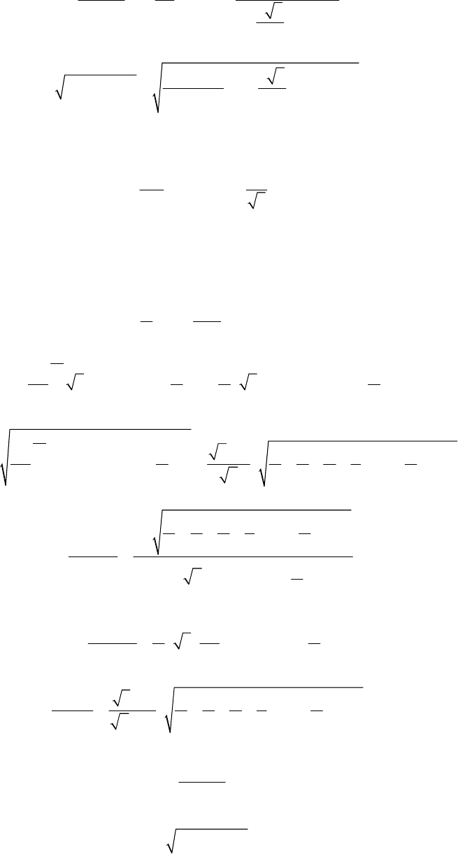
()
()
()
()
2
2
2
19 1
cos
33
1cos2
2
FF
ηα α
α
π
α
π
⎛⎞
==⋅
⎜⎟
⎜⎟
⎝⎠
+
⋅
(A.7)
() ()
()
()
2
2
2
33
11cos1
2
9cos
RF FF
π
αα α
π
α
⎡
⎤
=−= ⋅+ −
⎢
⎥
⋅
⎢
⎥
⎣
⎦
. (A.8)
Average and r.m.s. thyristor currents:
DC
L
F(AV) F(rms)
3
3
I
I
II==. (A.9)
A.2 Discontinuous conduction
The discontinuous conduction condition is defined by
2
33
ππ
α
⋅
<≤
(A.10)
()
2
3
DC S S
63
3sin d 3 1cos
23 3
VV(t)tV
π
α
ππ
αϖ α
ππ
⎡
⎤
⎛⎞
=⋅⋅+=⋅⋅⋅++
⎜⎟
⎢
⎥
⎝⎠
⎣
⎦
∫
(A.11)
()
2
3
22
S
LS
3
661
3 sin d sin2
233243
2
V
VVtt
π
α
ππαπ
αϖ α
ππ
⎡
⎤
⋅
⎛⎞ ⎛⎞
=⋅⋅+=⋅⋅−+⋅+
⎜⎟ ⎜⎟
⎢
⎥
⎝⎠ ⎝⎠
⎣
⎦
∫
(A.12)
()
()
()
L
DC
61
sin2
324 3
321cos
3
V
FF
V
πα π
πα
π
α
α
α
π
α
⎡⎤
⎛⎞
⋅⋅−+⋅ +
⎜⎟
⎢⎥
⎝⎠
⎣⎦
==
⎡⎤
⎛⎞
⋅⋅+ +
⎜⎟
⎢⎥
⎝⎠
⎣⎦
(A.13)
()
()
DC
S
DC
LL
3
31cos
3
V
V
I
RR
α
π
αα
π
⎡
⎤
⎛⎞
==⋅⋅⋅++
⎜⎟
⎢
⎥
⎝⎠
⎣
⎦
(A.14)
()
()
L
S
L
L
L
3
61
sin2
324 3
2
V
V
I
R
R
α
πα π
αα
π
⎡
⎤
⋅
⎛⎞
== ⋅⋅−+⋅ +
⎜⎟
⎢
⎥
⋅
⎝⎠
⎣
⎦
(A.15)
()
()
2
1
FF
ηα
α
⎛⎞
=
⎜⎟
⎜⎟
⎝⎠
(A.16)
() ()
2
1RF FF
αα
=− . (A.17)
R. VISINTINI
180
Average and r.m.s. thyristor currents:
DC
L
F(AV) F(rms)
3
3
I
I
II==. (A.18)
Acknowledgements
I would like to thank my colleagues R. Fabris, M. Zaccaria and D. Zangrando for the helpful
discussions we had and for their comments on the topics presented in or related to this paper.
References
[1] F. Bordry et al., Soft switching (ZVZCS) high-current, low-voltage modular power converter
[13 kA, 16 V], Proc. EPE 2001, Graz.
[2]
S.A. Griffiths et al., A power converter overview for the diamond storage ring magnets, Proc.
EPAC 2002, Paris.
[3]
A.W. Kelley and W.F. Yadusky, Rectifier design for minimum line-current harmonics and
maximum power factor, IEEE Trans. Power Electron.
7 (1992) 332.
[4]
A.W. Kelley and W.F. Yadusky, Phase-controlled rectifier line-current harmonics and power
factor as a function of firing angle and output filter inductance, Proc. APEC’90.
[5]
J.W. Kolar, Status of the techniques of three-phase PWM rectifier system with low effects on
the mains, Tutorial Notes at EPE 99, Lausanne.
[6]
IEEE Trans. Indust. Electron. 46 Nos. 3 and 4 (June 1999, August 1999).
[7]
M.H. Rashid (ed.), Power Electronics Handbook (Academic Press, 2001).
[8]
B.M. Bird, K.G. King and D.A.G. Pedder, An Introduction to Power Electronics, second
edition (Wiley, Chichester, 1992).
[9]
P.C. Sen, Power Electronics (Tata McGraw-Hill, 1988).
[10]
J. Schaefer, Rectifier Circuits: Theory and Design (Wiley, 1965).
[11]
D.G. Fink, H.W. Beaty, Standard Handbook for Electrical Engineers, twelyth edition
(McGraw-Hill, New York, 1987).
[12]
R.S. Ramshaw, Power Electronics Semiconductor Switches (Chapman & Hall, London, 1993).
[13]
H.W. Ish, J.G. Pett and P. Proudlock, An overview of the LEP power converter system, Proc.
PAC 1987.
[14]
R. Cassel and M.N. Nguyen, A unique power supply for the PEPII Klystron at SLAC, Proc.
PAC 1997.
[15]
H. Bühler, Classification of Static Converters, CAS – Power Converters for Particle
Accelerators, Montreux, 1990 (CERN 90-07).
[16]
P. Proudlock, Achieving high performance, CAS – Power Converters for Particle Accelerators,
Montreux, 1990 (CERN 90-07).
[17]
G.J. Wakileh, Power Systems Harmonics (Springer, 2001).
[18]
H.U. Boksberger, Electrical networks and power converters, these Proceedings.
[19]
N. Mohan, T.M. Undeland and W.P. Robbins, Power Electronics (Wiley, New York, 1989).
RECTIFIERS
181
[20] S. Griffiths, Protection, interlocks and diagnostics, these Proceedings.
[21]
B. Godenzi, Protection, interlocks and personal safety, CAS – Power Converters for Particle
Accelerators, Montreux 1990 (CERN 90-07).
[22]
H. Buri, Leistungshalbleiter, BBC-Fachbuchreihe (Brown Boveri & Cie).
[23]
BBC, Silizium Stromrichter Handbuch (Brown Boveri & Cie., 1971).
[24]
D. Bulfone, R. Richter, R. Visintini, Technical specifications PS-1/89 of the power supplies for
the main magnets of Elettra’s storage ring, Sincrotrone Trieste internal report ST/M-TN-89/16
(June 1989).
[25] A. Pierantoni, Dimensioning of the power supplies for the main magnets of Elettra’s storage
ring, OCEM private communication, 1990.
[26]
Eupec, Rectifier diode D 2601N, BIP AC / SM PB, 2002-05-31, Eupec Data Sheet.
[27]
Eupec, Phase control thyristor T 2871N, BIP AM / SM PB, 2002-04-07, Eupec Data Sheet.
[28]
Powerex Inc., FT1500AU-240 Ultra high voltage thyristor, Powerex Data Sheet.
[29]
R.W. Wall and H.L. Hess, Design and microcontroller implementation of a three-phase SCR
power converter, Idaho University, Department of Electrical Engineering Web Page
(www.ee.uidaho.edu/ee/rwall/3phase.html).
Bibliography
Most of the books reported as References cover almost all the topics of this lecture well beyond the
specific citation. I prefer to cite them again along with additional sources. As useful integration to
printed texts, it is possible to find on the Internet quite good educational sites dedicated to power
electronics applications. I have therefore included also some relevant URLs.
Books
CAS, Power Converters for Particle Accelerators, Montreux, 1990, (CERN 90-07).
M.H. Rashid (ed.), Power Electronics Handbook (Academic Press, 2001).
B.M. Bird, K.G. King and D.A.G. Pedder, An Introduction to Power Electronics, second edition
(Wiley, Chichester, 1993).
J. Schaefer, Rectifier Circuits: Theory and Design (Wiley, 1965).
P.C. Sen, Power Electronics (Tata McGraw-Hill, 1988).
N. Mohan, T.M. Undeland and W.P. Robbins, Power Electronics (Wiley, New York, 1989).
R.S. Ramshaw, Power Electronics Semiconductor Switches (Chapman & Hall, London, 1993).
B.R. Pelly, Thyristor Phase-Controlled Converters and Cycloconverters (Wiley, 1971).
C.W. Lander, Power Electronics, second edition (McGraw-Hill, London, 1987).
BBC, Silizium Stromrichter Handbuch (Brown Boveri & Cie, 1971).
H. Buri, Leistungshalbleiter, BBC-Fachbuchreihe (Brown Boveri & Cie).
G. Möltgen, Netzgeführte Stromrichter mit Thyristoren (Siemens, Erlangen, 1967) – Italian version: I
Tiristori (Etas Libri, 1974).
R. VISINTINI
182

URLs
http://www.epeec.ethz.ch/
http://www.ipes.ethz.ch/
http://www.powerdesigners.com/InfoWeb/resources/pe_html/contents.htm
http://users.telenet.be/educypedia/electronics/powerelectronics.htm
RECTIFIERS
183
