LOW-VOLTAGE BANDGAP REFERENCE DESIGN
UTILIZING SCHOTTKY DIODES
by
David L. Butler
A project
submitted in partial fulfillment
of the requirements for the degree of
Master of Science in Engineering, Electrical Engineering
Boise State University
March, 2005
© 2005
David L. Butler
ALL RIGHTS RESERVED
The project presented by David L. Butler entitled Low-Voltage Bandgap
Reference Design Utilizing Schottky Diodes is hereby approved:
__________________________________________
R. Jacob Baker Date
Advisor
__________________________________________
Said Ahmed-Zaid Date
Committee Member
__________________________________________
Nader Rafla Date
Committee Member
__________________________________________
John R. Pelton Date
Dean, Graduate College
ABSTRACT
As semiconductor device geometries continue to shrink, the corresponding voltage
applied across the processed devices must also be reduced. Therefore reference voltages
used in integrated circuits will need to have lower values. A typical bandgap reference
(BGR) voltage generator uses PN junction diodes or PNP BJT’s to bias the reference.
The forward bias voltage of these devices is typically 0.7 volts, and has a limiting effect
on circuit voltage and how low a reference voltage can be generated. Schottky, or metal-
semiconductor (MS), diodes have a lower forward bias voltage, typically of about 0.3
volts. The implementation of Schottky metal-semiconductor diodes in place of PN
diodes in the design of a BGR, should allow for lower reference voltage generation.
In this project, a BGR was designed and fabricated using a 0.5µm process. Schottky
diodes were also fabricated on the chip. After fabrication, the diodes were
experimentally characterized and modeled in SPICE. The SPICE model was used to
design a functional BGR. The BGR circuit with Schottky diodes was then tested and
validated as functional.
Measured results indicate a MS diode threshold voltage thermal characteristic of
-0.56mV/°C. With several parts evaluated, the BGR circuits produced a reference
voltage with a voltage gradient of a low of 7mV/V, to a high of 24mV/V, across a one
volt VDD sweep. Temperature coefficients ranging from -107ppm/°C to 500ppm/°C
were measured.
iv
TABLE OF CONTENTS
ABSTRACT……………………………………………………………………………...iv
LIST OF FIGURES……………………………………………………………………...vii
CHAPTER ONE: INTRODUCTION….………………………………………………….1
Introduction…………………………………………………………………………….1
CHAPTER TWO: SCHOTTKY DIODE.…………………………………………….......3
Schottky Diode Operation……………………………………………………………...3
Schottky Diode Fabrication Overview….……………………………………………...4
CHAPTER THREE: THEORY AND BGR DESIGN…………….…………………........5
Circuit Design………………………………………………………………………….5
Layout………………………………………………………………………………….7
Fabrication Process……………………………………………………………….......10
Schottky Diode Fabrication…………………………………………………………..11
Fabrication Results………………………………………………………………........12
CHAPTER FOUR: MEASURED RESULTS…………………….….………………….16
Diode Characterization……………………………………………………………….16
BGR Simulation………………………………………………………………………19
BGR Circuit Measurements…………………………………………………………..23
Diode Process Variation Evaluation………………………………………………….28
v
CHAPTER FIVE: CONCLUSION..…………………………………………………….31
Conclusion……………………………………………………………………………31
Future Work…………………………………………………………………………..31
REFERENCES…………………………………………………………………..………35
APPENDIX A: Final Design Netlist…………………………………………………….36
APPENDIX B: Future Design Netlist.…………………………………………………..40
vi
LIST OF FIGURES
Figure 2.1: MS Junction Energy Bandgap…………………………………….………….3
Figure 2.2: Schottky Diode Cross Section………………………….…………………….4
Figure 3.1: Bandgap Reference Circuit Design…………………….……………….……5
Figure 3.2: Chip Layout……………………………………………….…………….……8
Figure 3.3: Schottky Diode Layout……………………………………………………….9
Figure 3.4: BGR Circuit Layout…………………………………………………….......10
Figure 3.5: Full Chip Photo………………………………………….………………….13
Figure 3.6: Schottky Diode Photo……………………………………………………….14
Figure 3.7: BGR Circuit Photo………………………………………….………………15
Figure 4.1: Schottky Diode I-V vs. Temperature……………………………………….17
Figure 4.2: MS Diode I-V Curve Model………………………………………………...18
Figure 4.3: BGR Simulation Results……………………………………………………22
Figure 4.4: Final BGR Design…………………………………………………………..23
Figure 4.5: Measured Reference Voltage……………………………………….............24
Figure 4.6: Pre-Post Trim Measurements……………………………………………….25
Figure 4.7: BGR Temperature Behavior………………………………………………...26
Figure 4.8: BGR Thermal Comparison………………………………………….…........27
Figure 4.9: MS Diode I-V Distribution………………………………………………….29
vii
Figure 4.10: MS Diode Vt Distribution……………………………………………........30
Figure 5.1: Future BGR Design……………………………………………………........32
Figure 5.2: Future BGR Simulation……………………………………………………..33
viii
1
CHAPTER ONE: INTRODUCTION
Introduction
As semiconductor device geometries continue to shrink, the corresponding voltage
applied across the processed devices must also be reduced. Therefore reference voltages
used in integrated circuits will need to be reduced as well. A typical bandgap reference
(BGR) voltage generator uses PN junction diodes or PNP BJT’s to bias the reference.
The forward bias voltage of these devices is typically 0.7 volts, and has a limiting effect
on how low a reference voltage can be generated, as well as how low a system voltage
can be applied. Schottky, or metal-semiconductor (MS), diodes have a lower forward
bias voltage, typically of about 0.3 volts. The implementation of Schottky metal-
semiconductor diodes in place of PN diodes in the design of the BGR, should allow for
lower reference voltage generation. This project consists of the design and simulation of
a BGR utilizing MS diodes, followed by fabrication and validation of the design.
The bandgap reference voltage generator is designed to provide a stable reference
voltage across the device operating temperature and voltage. The BGR should also be
functionally stable regardless of typical process variations. This circuit is a low voltage
reference design for short channel processes. The design uses a known BGR circuit, but
replaces the PN junction diodes, with MS diodes [1].
The BGR design validation process will involve several steps. First is to simulate the
design operability of the BGR after replacement of the PN diodes in the circuit with the
2
MS diodes. An approximated Schottky diode model will be used to estimate the actual
operation. The modeled circuit will then be laid out and fabricated in a short channel
CMOS process. The actual diodes and resistors will not be connected, but bonded in
after fabrication to allow for post fabrication circuit adjustments. Once the actual MS
diodes have been fabricated, the operational characteristics will be recorded and the
simulation SPICE model will be updated accordingly. With this more accurate diode
model, the BRG circuit design will then be further simulated to achieve an optimized
reference. Then the final circuit will be built and characterized. Design validation will
involve showing acceptable BGR operation, measured across nominal voltage,
temperature and process variations.
3
CHAPTER TWO: SCHOTTKY DIODE
Schottky Diode Operation
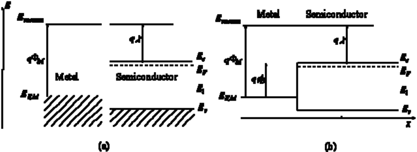
The Schottky, or metal-semiconductor (MS), diode is formed by the contact of a metal to
a semiconductor. The function of the Schottky diode operation differs from the PN
junction diode (most notably) in that it typically has a lower forward bias threshold
voltage. In this application, the lower threshold voltage is the advantageous feature.
When metal is contacted to a low dose N type semiconductor, electrons in the
semiconductor move into the metal, leaving behind holes and forming a potential charge
between the semiconductor and the metal [2]. This forms the rectifying contact of the
MS diode. An example of the resulting (a) pre and (b) post metal semiconductor contact
energy bandgap is shown in Figure 2.1 [3].
Figure 2.1 MS Junction Energy Bandgap
4
Although this explanation of the MS diode operation is perhaps oversimplified for the
purpose of developing a basic understanding of diode operation, there are many other
factors at work [4].
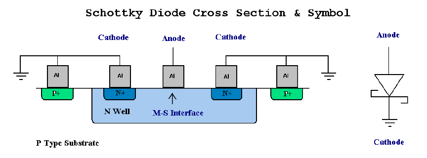
Schottky Diode Fabrication Overview
In this fabrication, the MS diode rectifying contact will be formed by deposition of a
metal (TiN/AlCu/TiN) on an N-well silicon. The ohmic contact will be made by
contacting the same N-well to metal but through an N+ active area. The ohmic contact
will then be routed to a ground plane. The cross section and accompanying schematic are
shown in Figure 2.2.
Figure 2.2 Schottky Diode Cross Section
The MS (rectifying) interface is located under the anode contact to the well. The
ohmic contact is formed in the N+ area. Here there are too many donor atoms to allow
for the formation of a depletion region. The cathode is connected to ground since the
operation of this circuit requires only forward bias operation.
5
CHAPTER THREE: THEORY AND BGR DESIGN
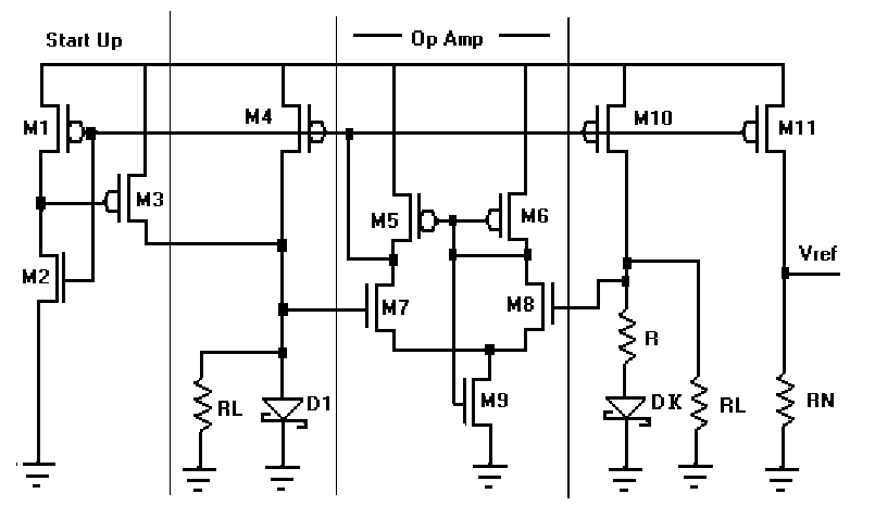
Circuit Design
The bandgap reference (BGR) voltage generator is designed to provide a stable reference
voltage across operating voltage and temperatures, while exhibiting minimum process
variation effects. This design uses a known BGR circuit, but replaces the PN junction
diodes, with MS diodes [1]. Since MS diodes have a lower forward bias voltage
(approximately 0.3V) than PN diodes (approximately 0.7V), this should allow for a lower
reference voltage generation. It will also allow the circuit to operate in a lower voltage
system. The general circuit design is shown here in Figure 3.1.
Figure 3.1 Bandgap Reference Circuit Design

6
The bandgap reference generates a stable voltage over temperature ranges utilizing
devices with properties that are proportional to absolute temperature (PTAT) and
complementary to absolute temperature (CTAT). PTAT properties are those that exhibit
increased current flow at increased temperature. CTAT are those that are
complementary. The circuits are used to complement each other thus providing for a
more stable temperature performance than is possible with each alone [1].
The portions of the circuit that operate proportional to absolute temperature are the
diodes D1 and diode DK along with its series resistor R. This is because the diode
voltage decreases with increasing temperature, allowing increased current flow through
the diode at higher temperatures. The PTAT current equation is given by Equation 3.1.
R
KnV
I
T
PTAT
ln*
=
EQ 3.1
The portions of the circuit that operates complementary to absolute temperature are
the resistors which are labeled as R*L. This is because the resistance increases with
increasing temperature, causing a reduction in the current flowing through the resistors at
higher temperatures.
LR
V
I
D
CTAT
*
1
= EQ 3.2

7
To some extent, this counters the increased current through the diodes and helps
stabilize the current flow through the reference making a more thermally stable reference
voltage. The overall temperature behavior of the BGR is modeled by the following
equation:
T
V
L
N
T
V
KNn
T
V
DTREF
∂
∂
+
∂
∂
=
∂
∂
1
**ln** EQ 3.3
Since the diodes in the circuit would have to be fabricated and characterized before the
circuit resistor values could be determined, the resistors would not be fabricated in the
layout, but would be applied externally after fabrication. The rest of the circuit (the
MOSFET portion) was designed based on SPICE simulation models, based on estimates
of the MS diodes anticipated operation [5]. The circuit was then ready for layout.
LAYOUT
The actual physical implementation of the design was layed out using the LASI layout
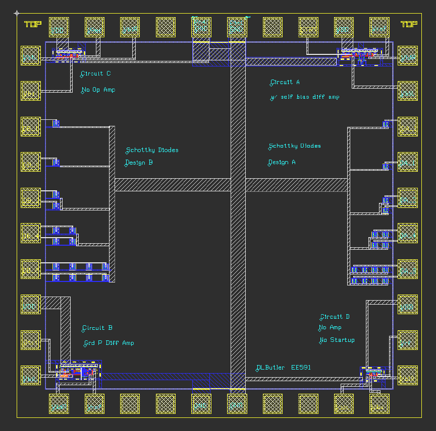
program [6]. The layout of the chips circuits were completed as shown in Figure 3.2.
The layout included four BGR circuits and two diode designs. Although the first design
is the one of focus, the other designs were included for redundancy in the event the first
circuit and diode designs did not function as expected. Since these other circuits and
diodes were not used in this project, they will not be mentioned further.
8
Figure 3.2 Chip Layout
The layout of the tested BGR circuit is the one in the top right corner of the layout.
The MS diodes that were used are on the right side. These were laid out as single diodes
of the same design. But to allow for larger multiple diodes for DK, (larger K) single
diodes were also grouped in clusters of 2, 4 and 8. These are referred to as x1, x2, x4,
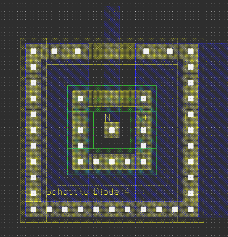
and x8 respectively. The diode layout in detail is shown in Figure 3.3.
9
Figure 3.3 Schottky Diode Layout
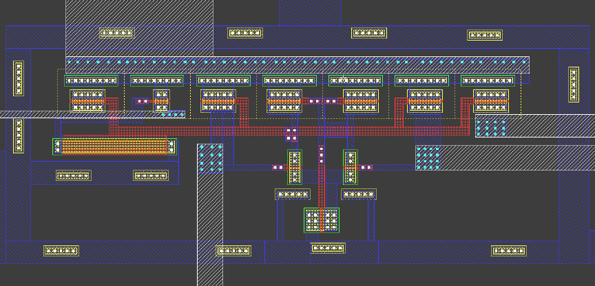
A close-up of the layout of the circuit that was tested can be seen in Figure 3.4. The
outputs are routed to bond pads as to allow for external manipulation of the circuit.
10
Figure 3.4 BGR Circuit Layout
Fabrication Process
The microchip was fabricated through a MOSIS fabrication organization [7]. The
specific fabrication facility was American Microsystems Inc. (AMI) [8]. The AMI
foundry produced the chip using their 0.5µm process designated AMI_C5F by MOSIS.
The Technology code is SCN3ME_SUBM. This defines the process as scalable CMOS
N-well with 3 metal layers and electrode (poly2) availability for capacitors. The SUBM
designation indicates the process is submicron. The process has a P-type substrate and
uses aluminum (TiN/AlCu/TiN) at metal levels.
The AMI process uses a scalable lambda design rule with minimum features of 2
lambda. This allows the same design features to be used across several different feature
size processes. Each lambda actual feature size is 0.3µm for this process series.
11
Therefore the minimum feature on this process run is 0.6µm, with the exception of
contacts and vias which are 0.5µm.
There are 17 fabrication mask layers available. These layers are the N-well, active,
poly, N+, P+, poly2, high resistance implant, four contact layers, Metal1, via1, Metal2,
via2, Metal3 and glass. Minimum design rules for feature size, spacing and overlaps vary
by specific levels.
The overall chips size was 1.5mm x 1.5mm. The 40 bond pads are 72µm x 72µm,
with a passivation opening of 60µm x 60µm. This is the minimum opening size for
bonding on this process.
The specific fabrication run that the chip was produced on is run number T4BP. The
die itself is “AE”, and five parts were produced. The run started on 11/29/04 and actually
entered fabrication on 12/06/04. After the parts completed fabrication, they were then
sent to a packager to be packaged in a 40pin DIP package. The packaged parts were
received back on 2/4/05.
Schottky Diode Fabrication
The AMI C5N process allows for the fabrication of the Metal Semiconductor diode.
Also known as a Schottky diode, the MS diode is (in this process) formed by first
creating an N-well in the P-type substrate. Then an opening to the silicon (through the
glass) of the N-well is created by the selection of the active layer. Unlike the more
common use of the active layer as an ohmic contact, no N+ implant is selected, but rather
12
a contact is selected and the metal is deposited on the N-well. This metal to low implant
N-well semiconductor forms a metal semiconductor rectifying diode.
The cathode of the diode is connected using a common ohmic contact. It is formed in
the same N-well by means of a contact. But in this case the N+ layer is selecting
facilitating a high N+ type implant to the active opening, which allows for a reduced
contact resistance. For this project, the ohmic contact is grounded. This ensures the
entire N-well is also tied to ground. Contacts are also applied around the N-well in the
substrate. The contacts are applied through an active and P+ layer to ensure the substrate
is also tied to ground. This reduces substrate injection which could cause voltage and
current fluctuations in the substrate that could alter the bias (possible a forward biasing)
of the diode, or possibly affecting other circuits.
The MS diode has an estimated area (metal to semiconductor contact area) of 0.25
square micrometers. This is since the contact size of this process is 0.5µm, thus
(0.5µm)*(0.5µm) = 0.25µm^2.
Fabrication Results
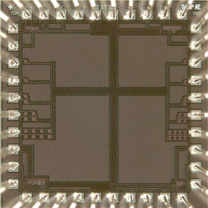
A photo of the fabricated and packaged chip is shown in Figure 3.5. Most visible are the
large ground busses that cross the die. Since there were few circuits fabricated, there was
ample room for significant and redundant grounding. Although all circuits and the
substrate shared the ground busses, individual circuits had their own power rails. This
would prevent a defect in one circuit from affecting other circuits on the chip.
13
Figure 3.5 Full Chip Photo
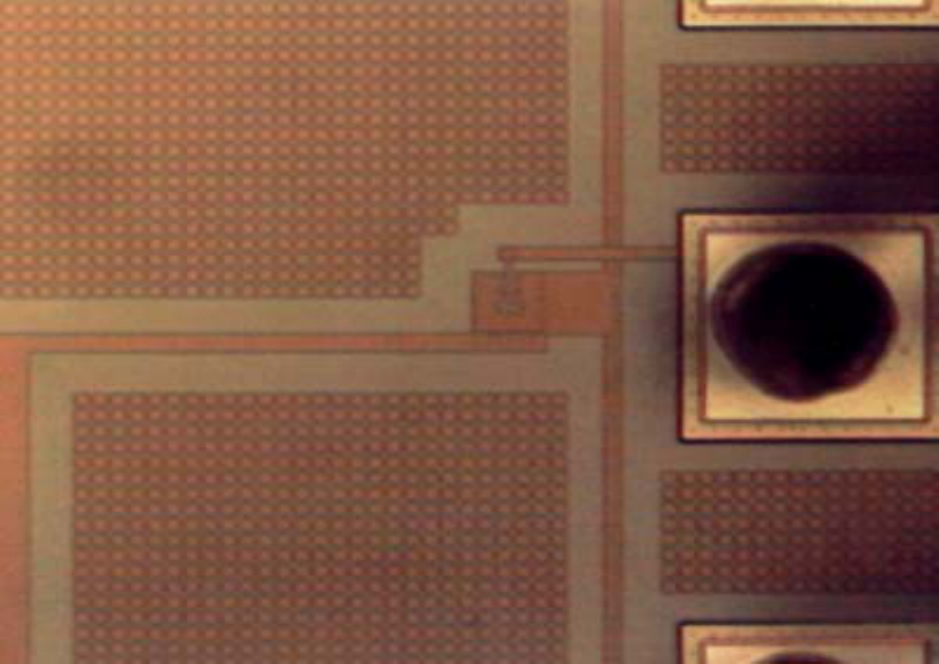
Although the individual circuits are not visible at such low magnification, a close up of
the MS diode and BGR circuit are included in Figure 3.6 and Figure 3.7 respectively.
14
Figure 3.6 Schottky Diode Photo
Metal fill can be seen around the diode structure; these are the small evenly placed
squares. They are used by the fabrication facility to ensure uniformity (level planarity)
during processing.
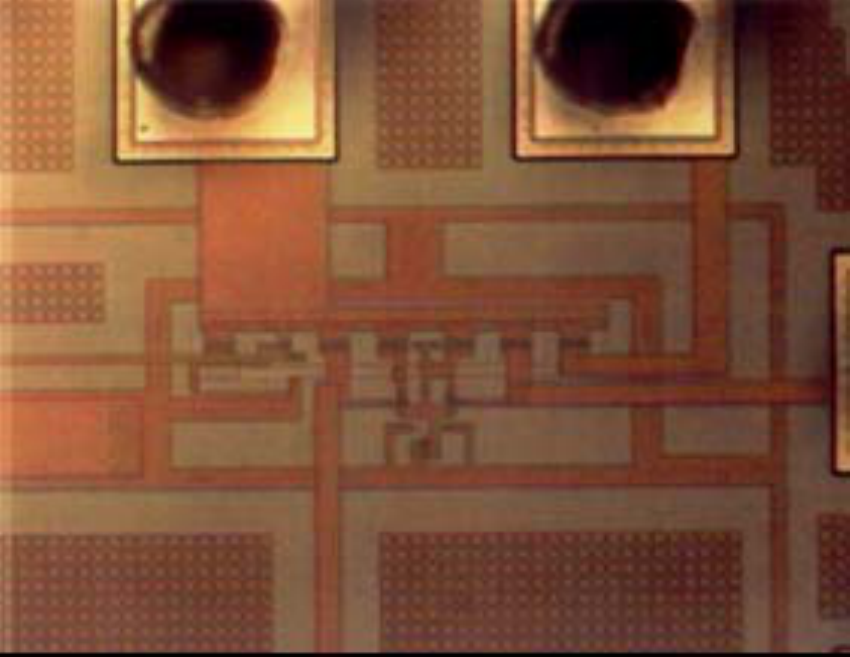
15
Figure 3.7 BGR Circuit Photo
This is the circuit as it was evaluated. Visible are the metal layers and several bond pads,
through which the circuit is accessed.

16
CHAPTER FOUR: MEASURED RESULTS
Diode Characterization
The Schottky diodes in the circuit were characterized to determine their actual
operational characteristics, in order to form a more precise diode model in SPICE. This
model would then be used in simulating the BGR circuit operation. Therefore a close
approximation of the MS diode model, and not an exact fit, was needed to get the BGR to
function. The diode current equation (ignoring series and shunt resistances) is given
below in Equation 4.1 [9]. Since the operation of this circuit does not involve reverse
bias components, these were not characterized.
⎟
⎟
⎠
⎞
⎜
⎜
⎝
⎛
−
⎭
⎬
⎫
⎩
⎨
⎧
= 1exp
nkT
qV
II
D
sD
EQ 4.1
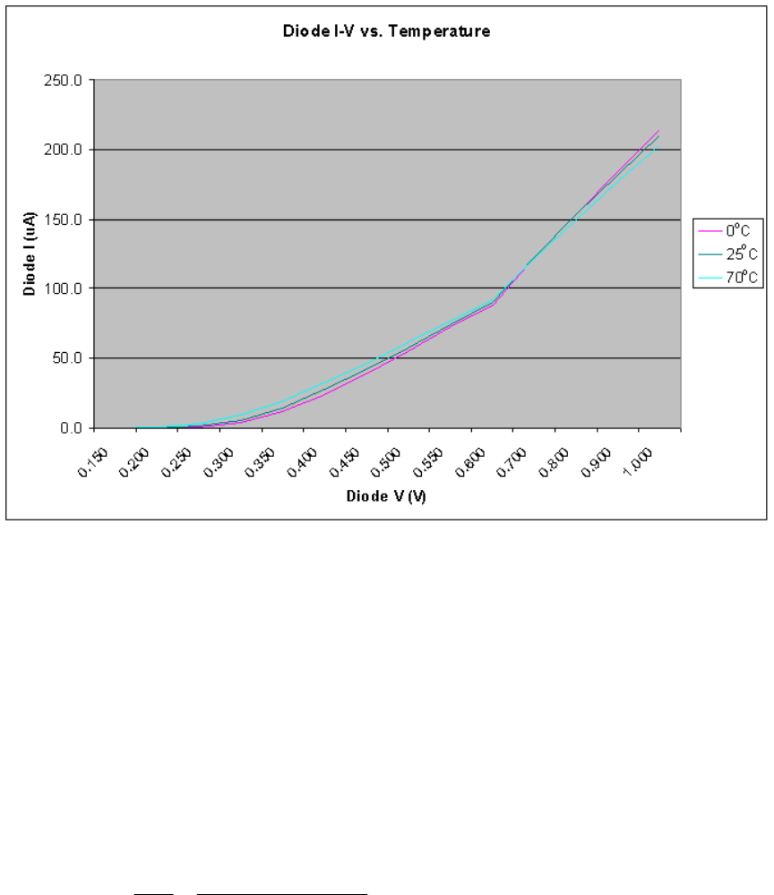
The tests run were voltage sweeps. These were run across operating voltage and
temperature, in order to determine current-voltage (I-V) curves over input voltage range
and temperature. This first test was run from 0V volt to 1.0V, and at 0°C, 25°C and
70°C. Since the area of operation that is of interest for the BGR is below 0.6V, all future
measurements were from 0V to 0.6V. Figure 4.1 shows the resulting measured I-V
characteristics of a single diode.
17
Figure 4.1 Schottky Diode I-V vs. Temperature
Note that there is a thermal crossover at about 0.75V, this is due to the internal resistance
in the diode, which allows the IR component of the current equation to dominate at
higher voltages. That is why low voltage operation is preferred.
This measured data was used to determine a temperature coefficient. It is evident that
the diode change in voltage with temperature is CTAT, as determined by equation 4.2.
minmax
minmax
@@
TT
TVTV
T
V
D
−
−
=
∂
∂
EQ 4.2
The measured averaged results on two diodes indicated that the value is –0.56 mV/°C.
This was determined by using a set current and measuring the voltage at 0°C and 70°C.
In this case three currents were used (3µA, 5µA and 10µA) and the results were
18
averaged. This brings up the point, that although most devices functioned similarly, there
was significant current and thermal variation between diodes.
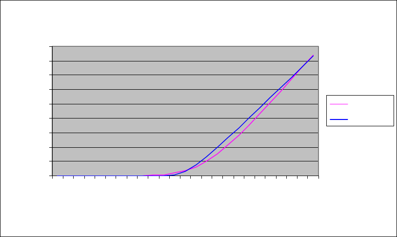
Based on measured results, the MS diode resistance was determined to be
approximately 3.2kΩ. This was determined by the slope of the I-V curve from 0.4V to
0.6V, since the series resistance is one divided by the slope of the I-V curve. The ideality
factor (n) and saturation current (Is) were estimated by applying values to the SPICE
simulation, and modeling it to the actual measured curve. Using this method, n was
determined to be approx 0.41 and Is was set to
18
10*4
−
A. The resulting simulation is
shown in Figure 4.2, overlaid with the average I-V curve of several measured diodes.
Diode Measured vs. Modeled
0.0
10.0
20.0
30.0
40.0
50.0
60.0
70.0
80.0
90.0
0.
0
00
0.050
0.100
0.
1
50
0.200
0.250
0.300
0.350
0.400
0.450
0
.
500
0
.
550
0.600
Diode V (V)
Diode I (uA)
Measured
Modeled
Figure 4.2 MS Diode I-V Curve Model

19
BGR Simulation
With this close approximation of the diode behavior modeled in SPICE, the BGR circuit
was then designed. The values of the resistor R, and ratios N and L, were calculated as
follows and used in the model, with the R*N (Rref) value being trimmed as needed for
the best performance. A value of 8 was used for K, as the largest diode structure
fabricated had eight individual diodes.
As noted earlier, the BGR thermal behavior is shown in Equation 4.3 [1].
T
V
L
N
T
V
KNn
T
V
DTREF
∂
∂
+
∂
∂
=
∂
∂
1
**ln** EQ 4.3
With the diode measurements taken relative to temperature (as previously noted), the
diode thermal derivates was determined to be:
=
∂
∂
T
V
D1
-0.56mV/°C
Since the design involved unknown resistor values, external 1/8W carbon film resistors
were implemented. The thermal effect was minimal because of the ratios used in the
design, and is expected to be minimal on actual fabricated resistors.
=
∂
∂
T
V
T
0.085mV/°C
With this information, and setting the temperature coefficient (TC) to zero (desired), the
following were solved for. First L is determined through the following equation:
T
V
Kn
T
V
L
T
D
∂
∂
∂
∂
−
=
*ln*
1
EQ 4.4

20
L =
085.0*08.2*41.0
56.0
= 7.7
Next N was solved as is indicated in the following equation:
L
V
KnV
V
N
D
T
REF
1
ln* +
= EQ 4.5
7.7
3.0
08.2*026.0*41.0
4.0
V
V
N
+
=
= 6.6
With the diode current estimated at 1µA, R was solved for from the following equation:
I
KVn
R
T
ln**
=
EQ 4.6
6
101
08.2*026.0*41.0
−
=
x
R
= 22kΩ
With these values, resistors were set as follows:
R*L = 22kΩ*7.7 = 172kΩ
R*N = 22kΩ*6.6 = 145kΩ
Since the goal was to develop a low voltage reference, a voltage of 0.4 volts was selected
as a target. This is an arbitrary point, but it is within the low voltage arena that is the
desirable area of operation. The target operating voltage (VDD) range was from 2.0V to
3.0V. It should be noted that the 0.5µm AMI process used in the fabrication of the chip
is a 3.3V-5.0V process, and not a low voltage process. A process temperature range of
0°C to 70° was used as the temperature range of evaluation. This is the standard cell data
sheet range of operation for this process.
21
Based on these criteria, and through simulation trial and error, Rref was initially set to
35kΩ instead of the calculated 145kΩ. Simulation indicated that at Rref of 145kΩ, the
output voltage was closer to 0.7V. This variation is mostly due to the estimate made of
the diode current in the calculation (set at 1µA) vs. the later measured Idiode of
approximately 3µA. Thus a value of 35kΩ was used, with Rref being refined later once
the actual results could be evaluated. This 35kΩ value provided a starting point for the
evaluation. The final SPICE netlist is included as attachment A.
The final circuit was simulated resulting in the simulated results shown in Figure 4.3.
The starting point varies because the startup circuit used in the design varies with
temperature. Because the startup circuit was considered a potential problem during the
preliminary design phase, it was bonded out in the actual layout so the BGR could be
evaluated independently of the startup circuit.
22
Figure 4.3 BGR Simulation Results
The final circuit was then built using the values for R, N and L based on these simulation
results, as shown in Figure 4.4.
23
Figure 4.4 Final BGR Design
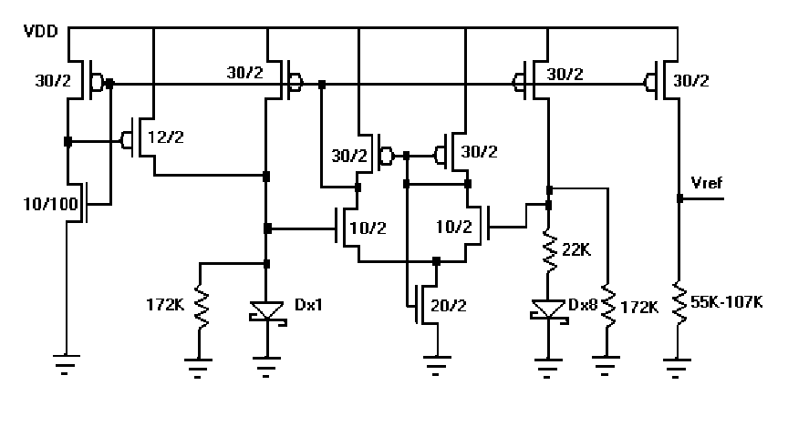
Note that Rref values differ from the original 35kΩ, and varies over a 53kΩ range. These
values were final trimmed values.
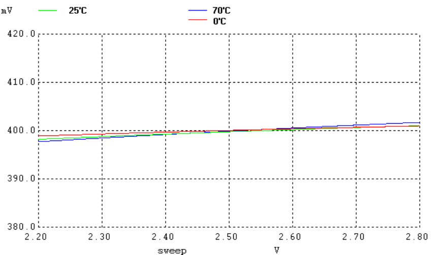
BGR Circuit Measurements
The first part was measured, resulting in a Vref of 0.251V. The resulting output voltage
of 0.251V at a VDD of 2.5V was lower than desired. It was expected to be necessary to
“trim” the output resistor (Rref) to tune the circuit. Once Rref was trimmed to 54.8kΩ,
the output shown in Figure 4.5 was produced.
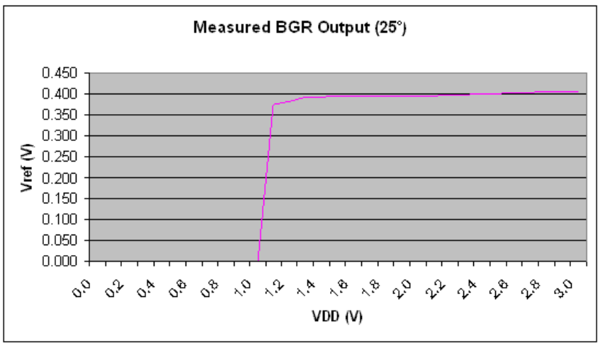
24
Figure 4.5 Measured Reference Voltage
The resulting output was relatively stable over the operating range of 2.0V to 3.0V. The
startup circuit was toggled in until the circuit started (at approx 1.1V) and was then
disconnected. The circuit current was approximately 23.75µA at 2.5V VDD and 25°C.
To examine process variation effects, all four functional parts were measured using
designed initial conditions, and again after they were trimmed. (Although five parts were
fabricated, only four were functional.) No failure analysis was performed on the failing
circuit. The pre-post trim results can be seen in Figure 4.6.
25
Figure 4.6 Pre-Post Trim Measurements
The four parts initially (as set based on the SPICE model) had a lower than simulated
reference voltage, and over a range of almost 80mV. These are the four lower lines in the
figure. An obvious process variation is evident. Although some measurement error is
always present, it is not expected to account for such a large distribution. It should be
noted that later refinement of the SPICE model and diode model brought the simulation
mean closer to 0.4V at 2.5V VDD.
Once the parts were trimmed to 0.4V at 2.5V VDD, (with an external resistor Rref)
the resulting reference voltages were very consistent over the operating range. These are
the four upper lines displayed in Figure 4.6. They overlap and appear as almost one line.
Over the operating voltage range (from 2.0V to 3.0V VDD), the reference voltage shift
across the four parts were 7mV, 8mV, 14mV and 24mV.
Vref Pre-Post Trim (All Parts)
0.000
0.050
0.100
0.150
0.200
0.250
0.300
0.350
0.400
0.450
2.00 2.50 3.00
VDD (V)
Vref (V)
Part 1 PRE
Part 3 PRE
Part 4 PRE
Part 5 PRE
Part 1 POST
Part 3 POST
Part 4 POST
Part 5 POST
26
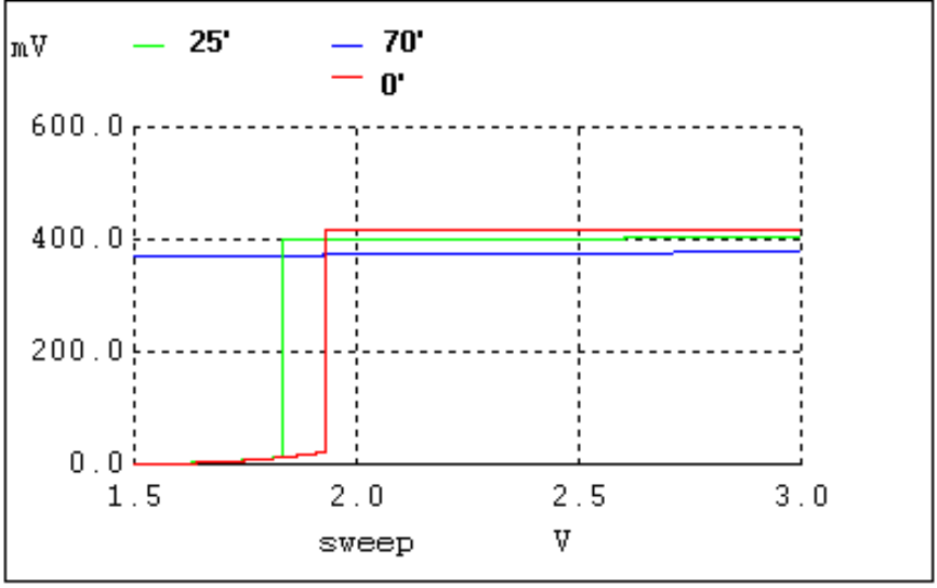
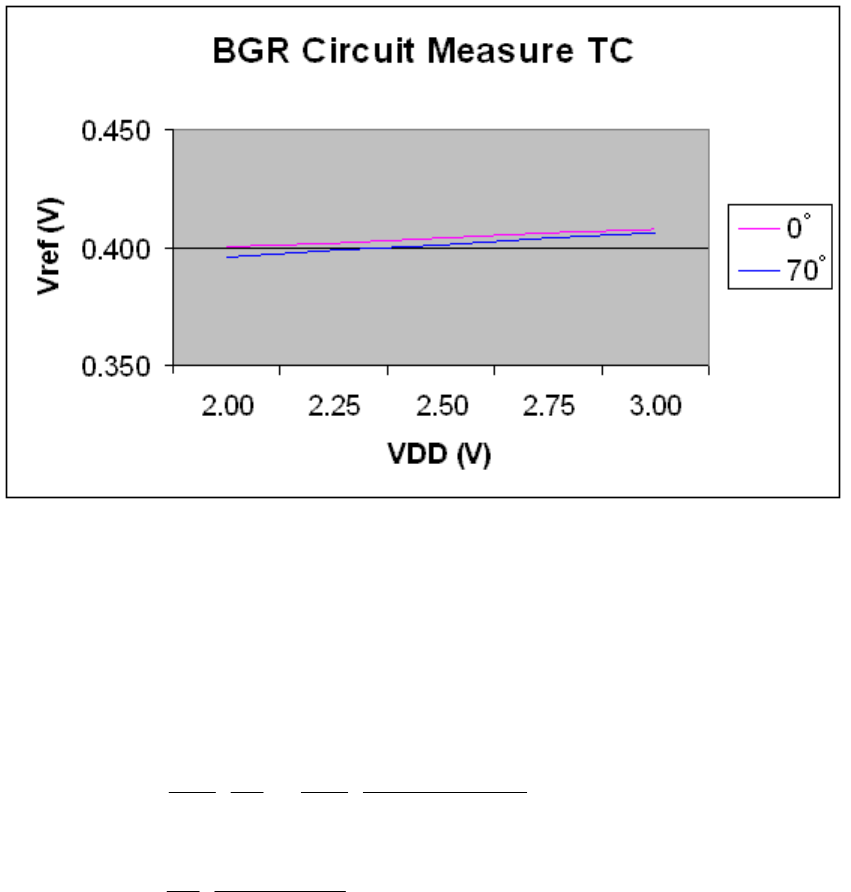
The temperature effects were also evaluated. Figure 4.7 shows the operation of the
circuit as measured at 0°C and at 70°C.
Figure 4.7 BGR Temperature Behavior
As is evident in Figure 4.7, there is little temperature variation between the minimum and
maximum operating ranges. The TC of this part was calculated at 2.5V VDD using
Equation 4.7 [8].
6
minmax
minmax
10*
11
⎟
⎟
⎠
⎞
⎜
⎜
⎝
⎛
−
−
=
⎟
⎠
⎞
⎜
⎝
⎛
∂
∂
=
TT
VV
VT
V
V
TC
REFREF
REFREF
EQ 4.7
6
10*
070
404.0401.0
4.0
1
⎟
⎠
⎞
⎜
⎝
⎛
−
−
=TC = -107ppm/°C
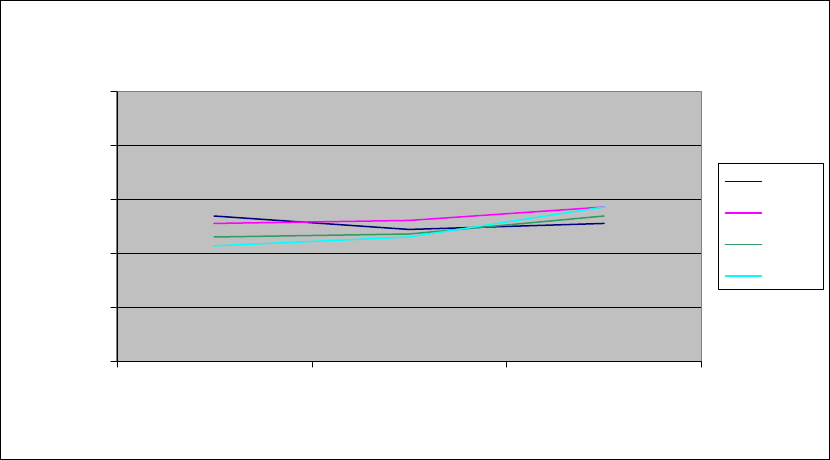
27
This is better than simulation results indicated, and indicates a voltage variation of only
43µV/°C. Other parts tested were 214, 286, and 500ppm/°C.
Figure 4.8 BGR Thermal Comparison
Again note the variation between devices. These measurements (as well as the earlier
voltage measurements) were taken in the same socket using the same external
components and test apparatus. The only external variation was the resistance trim
applied to the Rref resistor.
As a final evaluation, the external resistor Rref on one part was trimmed to achieve a
100mV Vref at 2.5V VDD. Although the circuit resistor values were not optimized for
this reference voltage, the BGR was evaluated simply at 25°C to determine if
functionality was possible at this voltage by trimming alone. Resistor Rref was trimmed
Vref vs. Temp (All Parts)
0.350
0.370
0.390
0.410
0.430
0.450
0' 25' 70'
Test Temp ('C)
Vref (V)
Part 1
Part 3
Part 4
Part 5
28
at 2.5V to 23.14kΩ, where Vref was at 0.10V. Over the 2.0V to 3.0V VDD range, the
circuit operated well, with Vref varied only 2.2mV over the 1.0V range.
Diode Process Variation Evaluation
Initially only a few diodes were evaluated, to get an approximated SPICE model so the
circuit could be simulated, since the BGR design is the fundamental object of this study.
But too explore the reason behind the circuit variations, further testing was conducted.
One BGR circuit was tested at 25°C and 2.5V VDD. It was set to a reference voltage of
400mV, then while all other factors remained the same (even the same diode set was used
for DK) the diode D1 was replaced one at a time with all other single functional diodes.
The Vref changed considerably as the BGR was operated with the different diodes
indicating that the diodes did contribute significantly to variations in the reference
voltage. Reference voltages ranged from 0.185V to 0.462V with D1 as the only variable.
Then all MS diodes I-V curves were measured over a 0V to 0.6V range at 25°C. The
modeling of all diodes using a HP 4156 parameter analyzer produced the graph shown in
Figure 4.9. Note the significant variation of the single diode (x1) distribution, and the
reducing distribution on the x2, x4 and then minimal distribution of the x8 diode
structures.
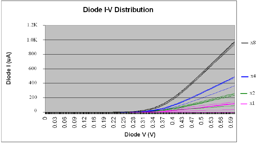
29
Figure 4.9 MS Diode I-V Distribution
Further, the diodes threshold voltages (Vt) were compared. For the purpose of equal
comparison, the diode threshold voltage was arbitrarily defined as where the diode
conducted 5µA of current. The results can be seen in Figure 4.10. Note the large
distribution of the single diodes vs. the smaller distribution of the x8 diode structures. It
should be noted that one single diode was excluded from this distribution as 5µA of
current was never achieved, even at 0.6V external voltage.
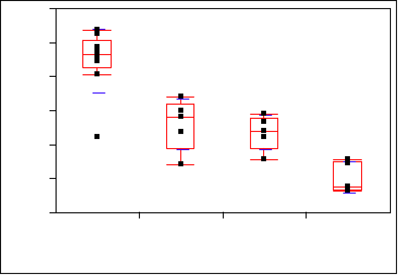
30
Vt
0.24
0.26
0.28
0.3
0.32
0.34
0.36
x1 x2 x4 x8
Diode
Figure 4.10 MS Diode Vt Distribution
The Vt point itself is lower for the multiple diode structures as is expected, since multiple
diodes are connected in parallel. In addition to allowing for a tighter distribution, this
attribute may also benefit the design as a lower diode Vt allows for lower reference
voltage generation. Based on these results, the diode model was modified to more
closely match these more quantitative results. (See appendix A.)
31
CHAPTER FIVE: CONCLUSION
Conclusion
The results indicate that the BGR design utilizing Schottky diodes was functional over
the intended operating voltage and temperature ranges. Further, the design actually
operated better than simulation results indicated, both in relation to temperature and
voltage behavior. Although there was evidence of significant initial condition variation
induced by process variation, the post trim results indicated this variation could be
minimized.
Future Work
During the course of the diode and circuit evaluation, it was discovered that there were
several areas that could offer BGR improvements. The three main areas of possible
improvement that were focused on are noted here.
1) Future work could be performed on the design of the same BGR circuit, but utilizing
multiple MS diode structures for D1 instead of a single diode. Multiples of DK would
also be utilized. Given the variations in the single diode, and the lack of variation of the
multiple diode structures, it appears that using multiple structures could help minimize
process variation effects and thus make the circuit operation more predictable. It would
also seem likely to have the effect of reducing the probability of a single diode defect
causing the circuit to fail, as an open (or high resistance) in one diode would be mitigated
32
by the operation of the other diodes. Another benefit would be the reduced Vt of the
multiple diode structure as seen in Figure 4.10, allowing for even lower Vref generation.
One concern is that higher current flow may be an issue.
Since there were few diode structures available for evaluation (only six in each of the
five devices), a comprehensive study of more diodes would be necessary to provide a
more statistically significant indication of the process capabilities and diode variation.
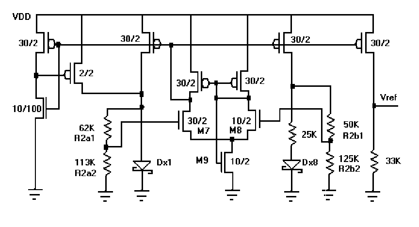
2) Another area that could be further investigated is the use of the circuit shown in
Figure 5.1, to generate a less temperature sensitive circuit, while generating a lower
reference voltage by using Schottky diodes [10]. This circuit design was proposed to
reduce the input common mode range of the added amplifier [1] [10].
Figure 5.1 Future BGR Design
33
This circuit was not tested directly, but simulations were performed that showed the
circuit would work with the modeled MS diodes. This circuit output displayed minimal
thermal variation over the operating range as can be seen in Figure 5.2. It is also
optimized (based again on simulation results) by increasing the width of M7 to 30
lambda, as well as increasing the resistance of R2a1 while reducing R2a2. This keeps the
total resistance equal to R2, but with the effect of lowering the Vg of M7. The net
simulation result is actually a thermal crossover at the point of interest (2.5V) as seen in
Figure 5.2. This would indicate a temperature coefficient of 0ppm/°C at that point. This
target may be further enhanced by allowing a trimming of R2a1 and R2a2 post
fabrication.
Figure 5.2 Future BGR Simulation

34
As can be seen in Equation 5.1 below, the lower MS diode voltage (replacing
2EB
V in the
equation with MS diode Vt) would result in a lower possible reference voltage [11].
⎟
⎟
⎠
⎞
⎜
⎜
⎝
⎛
⎥
⎦
⎤
⎢
⎣
⎡
+
+= K
R
RR
VV
R
R
V
AA
TEB
REF
REF
ln
2212
2
2
EQ 5.1
A SPICE netlist of the simulated circuit is included in appendix B.
3) Another area for improvement is in the application of the startup circuit. While that
component of the circuit was not the focus of the design evaluation, and therefore not
aggressively pursued, it would be necessary to have a more reliable startup circuit in an
actual design implementation of the BGR circuit in an application.
35
REFERENCES
1 R. Jacob Baker, “CMOS Circuit Design, Layout and Simulation” 2
nd
edition
Wiley Interscience, 2005 pp745-770
2 Karl Hess, “Advanced Theory of Semiconductor Devices”
IEEE Press, 2000 pp194-201
3 B. Van Zeghbroeck “Metal-Semiconductor Junctions” 2004
<http://ece-www.colorado.edu/~bart/book/book/chapter3/ch3_2.htm#3_2_2>
4 Leonard J. Brillson, “Contacts to Semiconductors, Fundamentals and
Technology” Noyes Publications, 1993 pp176-291
5 Ouse Tech, WinSpice Version 1.05.07
<http://www.winspice.co.uk/>
6 Dr. D. E. Boyce, LASI [Layout System for Individuals] Version 7.0.2.7
<
http://members.aol.com/lasicad/>
7 MOSIS “Low-Cost Prototyping and Small-Volume Production Service”
<http://www.mosis.org/>
8 AMIS [C5N Process]
<
http://www.mosis.org/products/fab/vendors/amis/c5/>
9 Dieter K. Schroder, “Semiconductor Material and Device Characterization”
2
nd
edition, Wiley Interscience, 1998 pp169-208
10 Ka Nang Leung & Philip K. T. Mok, “A Sub-1-V 15ppm/’C CMOS Bandgap
Voltage Reference Without Requiring Low Threshold Voltage Device”
IEEE Journal of Solid State Circuits, vol 37, no 4, April 2003 pp526-530
11 Ban P. Wong, et al., “Nano-CMOS Circuit and Physical Design”
Wiley Interscience, 2005 pp154-155
36
APPENDIX A
Final Design Netlist
37
Final Design Netlist
.control
destroy all
set temp=0
run
set temp=25
run
set temp=70
run
plot VDD dc1.vrf dc2.vrf dc3.vrf
plot dc1.vrf dc2.vrf dc3.vrf xlimit 1.9 3.0 ylimit 0 0.5
.endc
.option scale=0.3u
.dc VDD 0 3.0 1m
VDD VDD 0 DC 3.0V
M1 V1 Vbs VDD VDD CMOSP L=2 W=30
M2 V1 Vbs 0 0 CMOSN L=100 W=10
M3 V2 V1 VDD VDD CMOSP L=2 W=12
M4 V2 Vbs VDD VDD CMOSP L=2 W=30
M5 Vbs V4 VDD VDD CMOSP L=2 W=30
M6 V4 V4 VDD VDD CMOSP L=2 W=30
M7 Vbs V2 V3 0 CMOSN L=2 W=15
*modeled as W=15 to get circuit to start
M8 V4 V5 V3 0 CMOSN L=2 W=10
M9 V3 V4 0 0 CMOSN L=2 W=20
M10 V5 Vbs VDD VDD CMOSP L=2 W=30
M11 Vrf Vbs VDD VDD CMOSP L=2 W=30
R1 V2 0 RMODEL 172k
R2 V5 V6 RMODEL 22k
R3 V5 0 RMODEL 172k
R4 Vrf 0 RMODEL 60k
D1 V2 0 SCHOTTKY
D2 V6 0 SCHOTTKY 8
* T4BP SPICE BSIM3 VERSION 3.1 PARAMETERS
*SPICE 3f5 Level 8, Star-HSPICE Level 49, UTMOST Level 8
* DATE: Jan 31/05
* LOT: T4BP WAF: 9104
* Temperature_parameters=Default
.MODEL SCHOTTKY D IS=7e-18 N=0.43 XTI=3 RS=2.2K TC1=-0.002
.MODEL RMODEL R TC1=0.002
.MODEL CMOSN NMOS LEVEL = 8
38
+TNOM = 27 TOX = 1.42E-8
+XJ = 1.5E-7 NCH = 1.7E17 VTH0 = 0.5873345
+K1 = 0.9230324 K2 = -0.1047761 K3 = 22.4916147
+K3B = -9.1266087 W0 = 1E-8 NLX = 2.000399E-9
+DVT0W = 0 DVT1W = 0 DVT2W = 0
+DVT0 = 2.2994082 DVT1 = 0.4970166 DVT2 = -0.1842143
+U0 = 446.7488201 UA = 1E-13 UB = 1.299367E-18
+UC = 1.248923E-13 VSAT = 1.59167E5 A0 = 0.6101847
+AGS = 0.1302919 B0 = 2.533749E-6 B1 = 5E-6
+KETA = -1.666578E-3 A1 = 3.485566E-4 A2 = 0.3674233
+RDSW = 1.368085E3 PRWG = 0.0600883 PRWB = 0.0171806
+WR = 1 WINT = 2.09488E-7 LINT = 7.220693E-8
+XL = 1E-7 XW = 0 DWG = 2.605489E-9
+DWB = 4.277159E-8 VOFF = -0.0115079 NFACTOR = 0.7015054
+CIT = 0 CDSC = 2.4E-4 CDSCD = 0
+CDSCB = 0 ETA0 = 0.0031556 ETAB = -4.218915E-3
+DSUB = 0.4129659 PCLM = 2.4387548 PDIBLC1 = 1
+PDIBLC2 = 4.31964E-3 PDIBLCB = 0.053704 DROUT = 0.9257597
+PSCBE1 = 6.241157E8 PSCBE2 = 1.459532E-4 PVAG = 0
+DELTA = 0.01 RSH = 83.1 MOBMOD = 1
+PRT = 0 UTE = -1.5 KT1 = -0.11
+KT1L = 0 KT2 = 0.022 UA1 = 4.31E-9
+UB1 = -7.61E-18 UC1 = -5.6E-11 AT = 3.3E4
+WL = 0 WLN = 1 WW = 0
+WWN = 1 WWL = 0 LL = 0
+LLN = 1 LW = 0 LWN = 1
+LWL = 0 CAPMOD = 2 XPART = 0.5
+CGDO = 1.92E-10 CGSO = 1.92E-10 CGBO = 1E-9
+CJ = 4.303837E-4 PB = 0.9074906 MJ = 0.4317275
+CJSW = 3.001226E-10 PBSW = 0.8 MJSW = 0.1714547
+CJSWG = 1.64E-10 PBSWG = 0.8 MJSWG = 0.1714547
+CF = 0 PVTH0 = 0.0628352 PRDSW = 346.0290637
+PK2 = -0.0296479 WKETA = -0.0177686 LKETA = -2.260032E-3
.MODEL CMOSP PMOS LEVEL = 8
+TNOM = 27 TOX = 1.42E-8
+XJ = 1.5E-7 NCH = 1.7E17 VTH0 = -0.9286607
+K1 = 0.5412389 K2 = 0.0128372 K3 = 11.1025735
+K3B = -0.8099316 W0 = 3.891267E-7 NLX = 1.278268E-8
+DVT0W = 0 DVT1W = 0 DVT2W = 0
+DVT0 = 2.2645652 DVT1 = 0.7212046 DVT2 = -0.1560945
+U0 = 200.0599104 UA = 2.439885E-9 UB = 1.928396E-21
+UC = -7.00689E-11 VSAT = 1.808499E5 A0 = 0.9334131
+AGS = 0.1371285 B0 = 2.423807E-7 B1 = 1.124249E-6
+KETA = -2.535624E-3 A1 = 9.577499E-5 A2 = 0.3
+RDSW = 3E3 PRWG = 0.0148859 PRWB = -0.0125106
+WR = 1 WINT = 2.409073E-7 LINT = 8.424942E-8
+XL = 1E-7 XW = 0 DWG = -1.818861E-9
+DWB = 2.399629E-8 VOFF = -0.0801078 NFACTOR = 0.4609732
+CIT = 0 CDSC = 2.4E-4 CDSCD = 0
+CDSCB = 0 ETA0 = 0.0372311 ETAB = -0.0981321
+DSUB = 1 PCLM = 2.1048606 PDIBLC1 = 0.0586727
+PDIBLC2 = 3.988846E-3 PDIBLCB = -0.0530319 DROUT = 0.2623986
+PSCBE1 = 5.313202E9 PSCBE2 = 5E-10 PVAG = 0
39
+DELTA = 0.01 RSH = 105.2 MOBMOD = 1
+PRT = 0 UTE = -1.5 KT1 = -0.11
+KT1L = 0 KT2 = 0.022 UA1 = 4.31E-9
+UB1 = -7.61E-18 UC1 = -5.6E-11 AT = 3.3E4
+WL = 0 WLN = 1 WW = 0
+WWN = 1 WWL = 0 LL = 0
+LLN = 1 LW = 0 LWN = 1
+LWL = 0 CAPMOD = 2 XPART = 0.5
+CGDO = 2.28E-10 CGSO = 2.28E-10 CGBO = 1E-9
+CJ = 7.334167E-4 PB = 0.9498634 MJ = 0.4952447
+CJSW = 2.898167E-10 PBSW = 0.99 MJSW = 0.3046906
+CJSWG = 6.4E-11 PBSWG = 0.99 MJSWG = 0.3046906
+CF = 0 PVTH0 = 5.98016E-3 PRDSW = 14.8598424
+PK2 = 3.73981E-3 WKETA = 8.333721E-3 LKETA = -6.867545E-3
.end
40
APPENDIX B
Future Design Netlist
41
Future Design Netlist
.control
destroy all
set temp=0
run
set temp=25
run
set temp=70
run
plot vdd Vrf dc1.vrf dc2.vrf dc3.vrf
plot dc1.vrf dc2.vrf dc3.vrf xlimit 2.25 2.75 ylimit 0.38 0.42
.endc
.option scale=0.3u
.dc VDD 0 3 1m
VDD VDD 0 DC 3V
M1 V1 Vbs VDD VDD CMOSP L=2 W=30
M2 V1 Vbs 0 0 CMOSN L=100 W=10
M3 V2 V1 VDD VDD CMOSP L=2 W=2
M4 V2 Vbs VDD VDD CMOSP L=2 W=30
M5 Vbs V4 VDD VDD CMOSP L=2 W=30
M6 V4 V4 VDD VDD CMOSP L=2 W=30
M7 Vbs Vn V3 0 CMOSN L=2 W=30
M8 V4 Vp V3 0 CMOSN L=2 W=10
M9 V3 V4 0 0 CMOSN L=2 W=10
M10 V5 Vbs VDD VDD CMOSP L=2 W=30
M11 Vrf Vbs VDD VDD CMOSP L=2 W=30
R1a V2 Vn RMODEL 62k
R1b Vn 0 RMODEL 113k
R2 V5 V6 RMODEL 25k
R3a V5 Vp RMODEL 50k
R3b Vp 0 RMODEL 125k
R4 Vrf 0 RMODEL 33.6k
D1 V2 0 SCHOTTKY
D2 V6 0 SCHOTTKY 8
* T4BP SPICE BSIM3 VERSION 3.1 PARAMETERS
*SPICE 3f5 Level 8, Star-HSPICE Level 49, UTMOST Level 8
* DATE: Jan 31/05
* LOT: T4BP WAF: 9104
* Temperature_parameters=Default
.MODEL SCHOTTKY D IS=4e-18 N=0.41 XTI=3 RS=3.3K
.MODEL RMODEL R TC1=0.002
42
.MODEL CMOSN NMOS LEVEL = 8
+TNOM = 27 TOX = 1.42E-8
+XJ = 1.5E-7 NCH = 1.7E17 VTH0 = 0.5873345
+K1 = 0.9230324 K2 = -0.1047761 K3 = 22.4916147
+K3B = -9.1266087 W0 = 1E-8 NLX = 2.000399E-9
+DVT0W = 0 DVT1W = 0 DVT2W = 0
+DVT0 = 2.2994082 DVT1 = 0.4970166 DVT2 = -0.1842143
+U0 = 446.7488201 UA = 1E-13 UB = 1.299367E-18
+UC = 1.248923E-13 VSAT = 1.59167E5 A0 = 0.6101847
+AGS = 0.1302919 B0 = 2.533749E-6 B1 = 5E-6
+KETA = -1.666578E-3 A1 = 3.485566E-4 A2 = 0.3674233
+RDSW = 1.368085E3 PRWG = 0.0600883 PRWB = 0.0171806
+WR = 1 WINT = 2.09488E-7 LINT = 7.220693E-8
+XL = 1E-7 XW = 0 DWG = 2.605489E-9
+DWB = 4.277159E-8 VOFF = -0.0115079 NFACTOR = 0.7015054
+CIT = 0 CDSC = 2.4E-4 CDSCD = 0
+CDSCB = 0 ETA0 = 0.0031556 ETAB = -4.218915E-3
+DSUB = 0.4129659 PCLM = 2.4387548 PDIBLC1 = 1
+PDIBLC2 = 4.31964E-3 PDIBLCB = 0.053704 DROUT = 0.9257597
+PSCBE1 = 6.241157E8 PSCBE2 = 1.459532E-4 PVAG = 0
+DELTA = 0.01 RSH = 83.1 MOBMOD = 1
+PRT = 0 UTE = -1.5 KT1 = -0.11
+KT1L = 0 KT2 = 0.022 UA1 = 4.31E-9
+UB1 = -7.61E-18 UC1 = -5.6E-11 AT = 3.3E4
+WL = 0 WLN = 1 WW = 0
+WWN = 1 WWL = 0 LL = 0
+LLN = 1 LW = 0 LWN = 1
+LWL = 0 CAPMOD = 2 XPART = 0.5
+CGDO = 1.92E-10 CGSO = 1.92E-10 CGBO = 1E-9
+CJ = 4.303837E-4 PB = 0.9074906 MJ = 0.4317275
+CJSW = 3.001226E-10 PBSW = 0.8 MJSW = 0.1714547
+CJSWG = 1.64E-10 PBSWG = 0.8 MJSWG = 0.1714547
+CF = 0 PVTH0 = 0.0628352 PRDSW = 346.0290637
+PK2 = -0.0296479 WKETA = -0.0177686 LKETA = -2.260032E-3
.MODEL CMOSP PMOS LEVEL = 8
+TNOM = 27 TOX = 1.42E-8
+XJ = 1.5E-7 NCH = 1.7E17 VTH0 = -0.9286607
+K1 = 0.5412389 K2 = 0.0128372 K3 = 11.1025735
+K3B = -0.8099316 W0 = 3.891267E-7 NLX = 1.278268E-8
+DVT0W = 0 DVT1W = 0 DVT2W = 0
+DVT0 = 2.2645652 DVT1 = 0.7212046 DVT2 = -0.1560945
+U0 = 200.0599104 UA = 2.439885E-9 UB = 1.928396E-21
+UC = -7.00689E-11 VSAT = 1.808499E5 A0 = 0.9334131
+AGS = 0.1371285 B0 = 2.423807E-7 B1 = 1.124249E-6
+KETA = -2.535624E-3 A1 = 9.577499E-5 A2 = 0.3
+RDSW = 3E3 PRWG = 0.0148859 PRWB = -0.0125106
+WR = 1 WINT = 2.409073E-7 LINT = 8.424942E-8
+XL = 1E-7 XW = 0 DWG = -1.818861E-9
+DWB = 2.399629E-8 VOFF = -0.0801078 NFACTOR = 0.4609732
+CIT = 0 CDSC = 2.4E-4 CDSCD = 0
+CDSCB = 0 ETA0 = 0.0372311 ETAB = -0.0981321
+DSUB = 1 PCLM = 2.1048606 PDIBLC1 = 0.0586727
43
+PDIBLC2 = 3.988846E-3 PDIBLCB = -0.0530319 DROUT = 0.2623986
+PSCBE1 = 5.313202E9 PSCBE2 = 5E-10 PVAG = 0
+DELTA = 0.01 RSH = 105.2 MOBMOD = 1
+PRT = 0 UTE = -1.5 KT1 = -0.11
+KT1L = 0 KT2 = 0.022 UA1 = 4.31E-9
+UB1 = -7.61E-18 UC1 = -5.6E-11 AT = 3.3E4
+WL = 0 WLN = 1 WW = 0
+WWN = 1 WWL = 0 LL = 0
+LLN = 1 LW = 0 LWN = 1
+LWL = 0 CAPMOD = 2 XPART = 0.5
+CGDO = 2.28E-10 CGSO = 2.28E-10 CGBO = 1E-9
+CJ = 7.334167E-4 PB = 0.9498634 MJ = 0.4952447
+CJSW = 2.898167E-10 PBSW = 0.99 MJSW = 0.3046906
+CJSWG = 6.4E-11 PBSWG = 0.99 MJSWG = 0.3046906
+CF = 0 PVTH0 = 5.98016E-3 PRDSW = 14.8598424
+PK2 = 3.73981E-3 WKETA = 8.333721E-3 LKETA = -6.867545E-3
.end
