
Department of Electronics and Communication Engineering Page 1
Name of Student:
Enrolment No.:
Class:
Section:
Session:
Digital Communication Lab
[EC-502]Manual
Department of Electronics and Communication Engineering
LAKSHMI NARAIN COLLEGE OF TECHNOLOGY
Kalchuri Nagar, Raisen Road Bhopal (MP) 462023

LAKSHMI NARAIN COLLEGE OF TECHNOLOGY, BHOPAL
Department of Electronics and Communication Engineering Page 2
Vision and Mission of the Department
Vision
To be recognized as Centre of Academic Excellence by imparting quality teaching
and strengthening research and development activities with world class
infrastructure in the field of Electronics and Communication Engineering.
Mission
• To establish a quality teaching learning process to provide application
oriented, in-depth knowledge consistently.
• To establish state-of-the-art laboratories for academic excellence and to
develop infrastructure through collaboration for quality research.
• To equip the students by blending theoretical knowledge and practical skills
with employability and entrepreneurship traits for a bright successful career.
• To inculcate team spirit and leadership qualities to produce socially acceptable,
eco-friendly and responsible citizens.
LAKSHMI NARAIN COLLEGE OF TECHNOLOGY, BHOPAL
Department of Electronics and Communication Engineering Page 3
Program Specific Outcomes (PSO’s)
• PSO1: Demonstrate ability to apply basic concepts of science and
engineering to undertake theoretical learning of Electronic Devices and
Circuits, Analog and Digital Communication, Signals and Systems,
Embedded Systems, VLSI Design etc..
• PSO2: Demonstrate application of acquired hands-on skills such as
Circuit Simulation, MATLAB, HDL Programming, Embedded Systems,
DSP and PCB Designing etc..
• PSO3: Work actively in teams who under take some research oriented
projects, especially development projects and a few industry sponsored
projects.
• PSO4: Learn extra-curricular courses such as soft-skills, personality
development and groom them as responsible citizen with professional ethics
blended with human values, engineering economics and sustainability to
handle real life problems.
Program Educational Objectives (PEO’s)
Student will be able to
• Apply knowledge of mathematics, science and engineering as appropriate in
the field of Electronics and Communication Engineering as proficient learners
in the domains such as Electronic Circuits, Embedded Systems, Communication
Systems, Digital Signal Processing, VLSI Design, Data Networks, IOT, and
Simulation etc.
• Seek admissions at Institutes of repute for higher education in Engineering
and Technology and Management to the tune of 10%, seek employment in core and
IT domains to the extent of 80% with remaining 10% opting for entrepreneurship.
• Use the skills, latest techniques, tools for modern engineering and ICT which
are necessary to analyze industrial problems related to Electronics and
Comm. Engineering with focus to Global, Economical and Environmental Issues.
• Understand engineering solutions, exhibit professionalism, ethical attitude, team
work, effective written and oral communication skills to practice in their profession
with high regards to societal issues and responsibilities.

LAKSHMI NARAIN COLLEGE OF TECHNOLOGY, BHOPAL
Department of Electronics and Communication Engineering Page 4
Course: DIGITAL COMM.LAB (EC502)
Course Outcomes (CO’s)
CO1. Analyze the process of converting analog signal to discrete form along with their circuits.
CO2. Analyze various Analogue to Digital conversion techniques along with various Line Coding
methods.
CO3. Compare various digital transmission techniques on the base of Spectral properties.
CO4. Develop an expression for probability of error of different digital communication techniques.
CO5. Design communication systems with optimum capacity.

LAKSHMI NARAIN COLLEGE OF TECHNOLOGY, BHOPAL
Department of Electronics and Communication Engineering Page 5
Code of Conducts for the Laboratory
• All bags must be left at the indicated place.
• The lab timetable must be strictly followed.
• Be PUNCTUAL for your laboratory session.
• Noise must be kept to a minimum.
• Workspace must be kept clean and tidy at all time.
• Handle the experiment kit and interfacing its with care.
• All students are liable for any damage to the accessories due to their own negligence.
• Students are strictly PROHIBITED from taking out any items from the laboratory.
• Students are NOT allowed to work alone in the laboratory without the Lab Supervisor
• Report immediately to the Lab Supervisor if any malfunction of the accessories, is there.
• Before leaving the lab Place the stools properly.
• Please check the laboratory notice board regularly for updates.

LAKSHMI NARAIN COLLEGE OF TECHNOLOGY, BHOPAL
Department of Electronics and Communication Engineering Page 6
Rubrics for Assessment of student performance during Experiments
Enrolment No.:
INDEX
Area of Direct
Assessment
Poor
(0-2
Marks)
Fair
(3-4
Marks)
Average
(5-6 Marks)
Good
(7-8 Marks)
Excellent
(9-10
Marks)
Aim &
Theory
Aim is not
clear and
irrelevant
theory written
Concept was
not explained.
Aim is clear
and Incomplete
theory written.
Concept could
not be
explained.
Aim is clear and
Theory written
but is
unorganized
Concept is
explained.
Aim is clear and
Theory written
properly.
Concept is
explained.
Aim is clear and
Theory written
properly.
Concept is
explained with
neat diagrams.
Performance
and Working
with Others
Did not
conduct the
experiment
and none of
the member
recorded the
observations.
Followed few
steps to conduct
the experiment.
But few
members
recorded the
observations.
Followed few
steps to conduct
the experiment.
Few members
recorded the
observations.
Followed step
by step method
to conduct the
experiment.
Sufficient
observations
recorded by all
team members.
Followed step
by step method
to conduct the
experiment.
Many
observations
recorded by all
team members.
Safety
Measures
None of the
team member
knew safety
measures and
did not
followed.
Team members
had knowledge
of safety
measures and
followed few of
them.
Team members
had fair
knowledge of
safety measures
and followed
them.
Team members
were well
acquainted with
safety measures
and followed.
Team members
were well
acquainted with
safety measures
and followed all
of them.
Result and
Conclusion
No data
recorded.
Conclusion
can not be
drawn.
Analysis does
not follow data
the data.
Conclusion can
not be drawn.
Analysis as
recorded
somewhat lacks
in insight. Results
is poorly recorded
to make sense.
Conclusion can
not be drawn.
Analysis as
recorded
somewhat lacks
in insight. But
clearly recorded
as Results.
Conclusion is
properly drawn.
Observations
are analyzed
accurately and
clearly recorded
as Results.
Conclusion is
properly drawn.
Observations
and
Calculations
No
observations
recorded and
no calculation
done.
Insufficient
number of
observations
recorded. So
calculations are
Inaccurate.
Sufficient number
of observations
recorded but
calculations are
Inaccurate.
Almost all
observations
recorded.
Calculations are
accurate and
well organized.
Many
observations
recorded in the
table.
Calculations are
accurate and
well organized.
Internal Viva
Student does
not have grasp
on the
experiment
and could not
answer the
questions
about the
experiment.
Student
mumbles
incorrectly,
pronouns terms
and speak too
quietly for
teachers to hear.
Student is
uncomfortable
but is able to
answer basic
questions about
the experiment.
Student is at
ease and able to
answer expected
questions, but
fails to
elaborate.
Student
demonstrated
full knowledge
by answering all
questions with
explanations
and elaboration.

LAKSHMI NARAIN COLLEGE OF TECHNOLOGY, BHOPAL
Department of Electronics and Communication Engineering Page 7
INDEX
Name of Student: Enrolment No.:
Sl.
No.
Title of the
Experiment
Date of
Experiment
Date of
Submission
Remark
1
Generation and Detection of
Sampled Signal.
2
Generation and Detection of
Time Division Multiplexed PAM.
3
Generation and Detection of
Pulse Code Modulation
4
Generation and Detection of
Delta Modulation
5
Generation and Detection of
FSK Modulated Signal.
6
Generation and Detection of
BPSK Modulated Signal.
7
Generation and Detection of
ASK Modulated Signal.
8
Generation and Detection of
DPSK Modulated Signal.
9
Generation and Detection of
QPSK Modulated Signal.
10
Generation and Detection of
Differential Pulse Code
Modulation
LAKSHMI NARAIN COLLEGE OF TECHNOLOGY, BHOPAL
Department of Electronics and Communication Engineering Page 8
Date of Experiment: _______________
EXPERIMENT NO:1
AIM:
To generate the Sampled signal and analyze the effect of variations in sampling rate over the recovered
message.
APPARATUSREQUIRED:
1. ST2101withpowersupplycord.
2. Oscilloscope with connecting probe.
3. Connecting cords.
THEORY:
The signals used in the real world, such as our voice, are called "analog" signals .To process these signals for
digital communication, there is a need to convert analog signals to "digital" form .While analog signal is
continuous in both time and amplitude , a digital signal is discrete in both time and amplitude .To convert
continuous time signal to discrete time signal, a process is used called as sampling. The value of the signal is
measured at certain intervals in time. Each measurement is referred to as a sample.
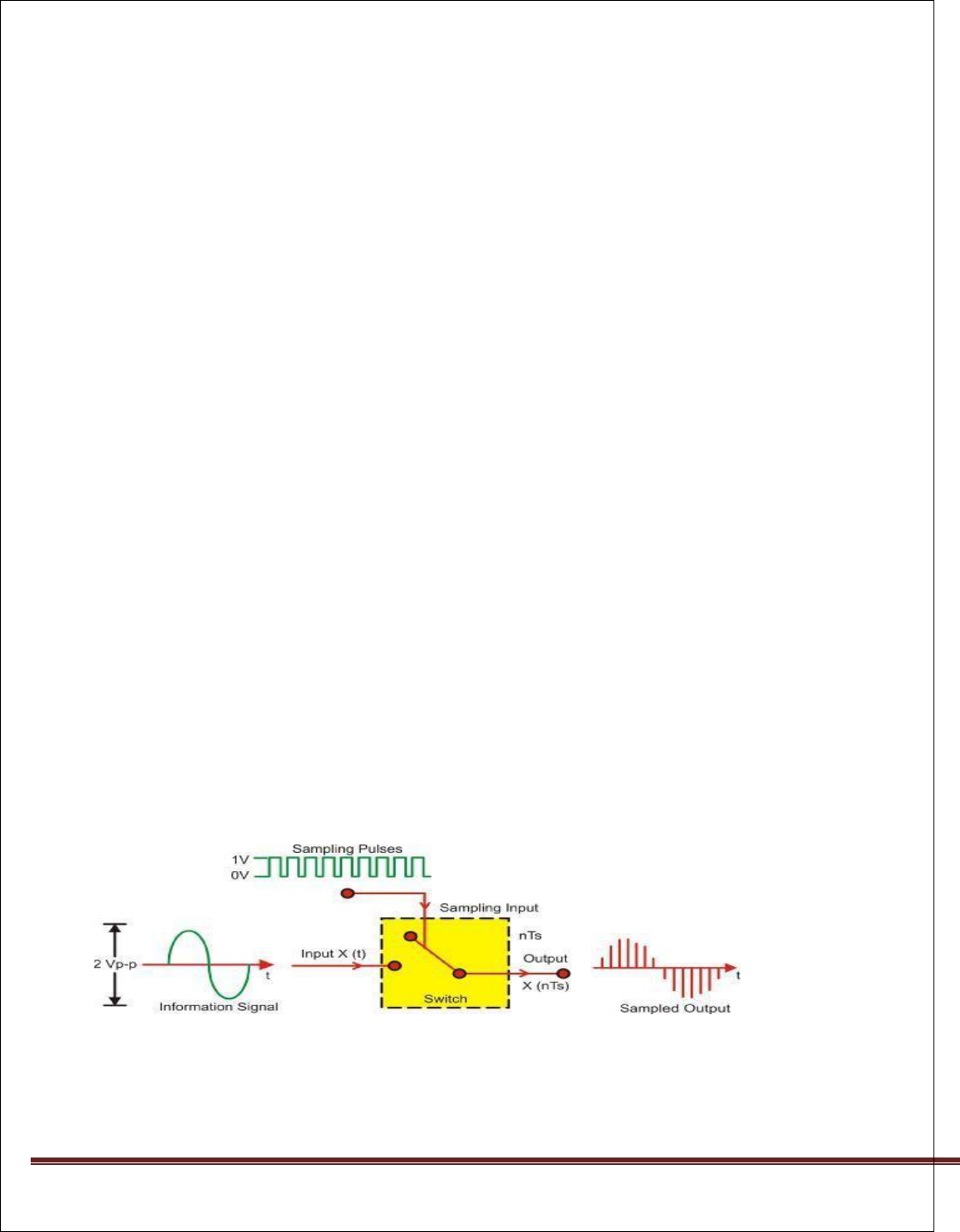
Principle of sampling:-
Consider an analogue signal x(t) that can be viewed as a continuous function of time, as shown in figure. We
can represent this signal as a discrete time signal by using values of x(t) at intervals of nTs to form x(nTs) as
shown in figure . We are “grabbing" points from the function x(t) at regular intervals of time, Ts, called the
sampling period.
A precondition of the sampling theorem is that the signal to be band limited. However, in practice, no time-
limited signal can be band limited. Since signals of interest are almost always time-limited (e.g., at most
spanning the lifetime of the sampling device in question), it follows that they are not band limited. However ,
by designing a sampler with an appropriate guard band, it is possible to obtain output that is as accurate as
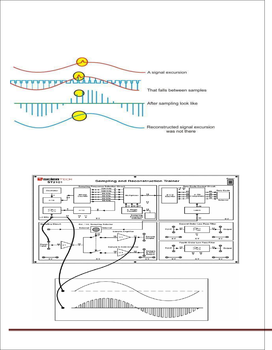
necessary. Aliasing is the presence of unwanted components in the reconstructed signal. These components
were not present when the original signal was sampled. In addition, some of the frequencies in the original
LAKSHMI NARAIN COLLEGE OF TECHNOLOGY, BHOPAL
Department of Electronics and Communication Engineering Page 9
signal may be lost in the reconstructed signal. Aliasing occurs because signal frequencies can overlap if the
sampling frequency is too low. As a result , the higher frequency components roll into the reconstructed
signal and cause distortion of the signal Frequencies "fold" around half the sampling frequency. This type of
signal distortion is called aliasing.
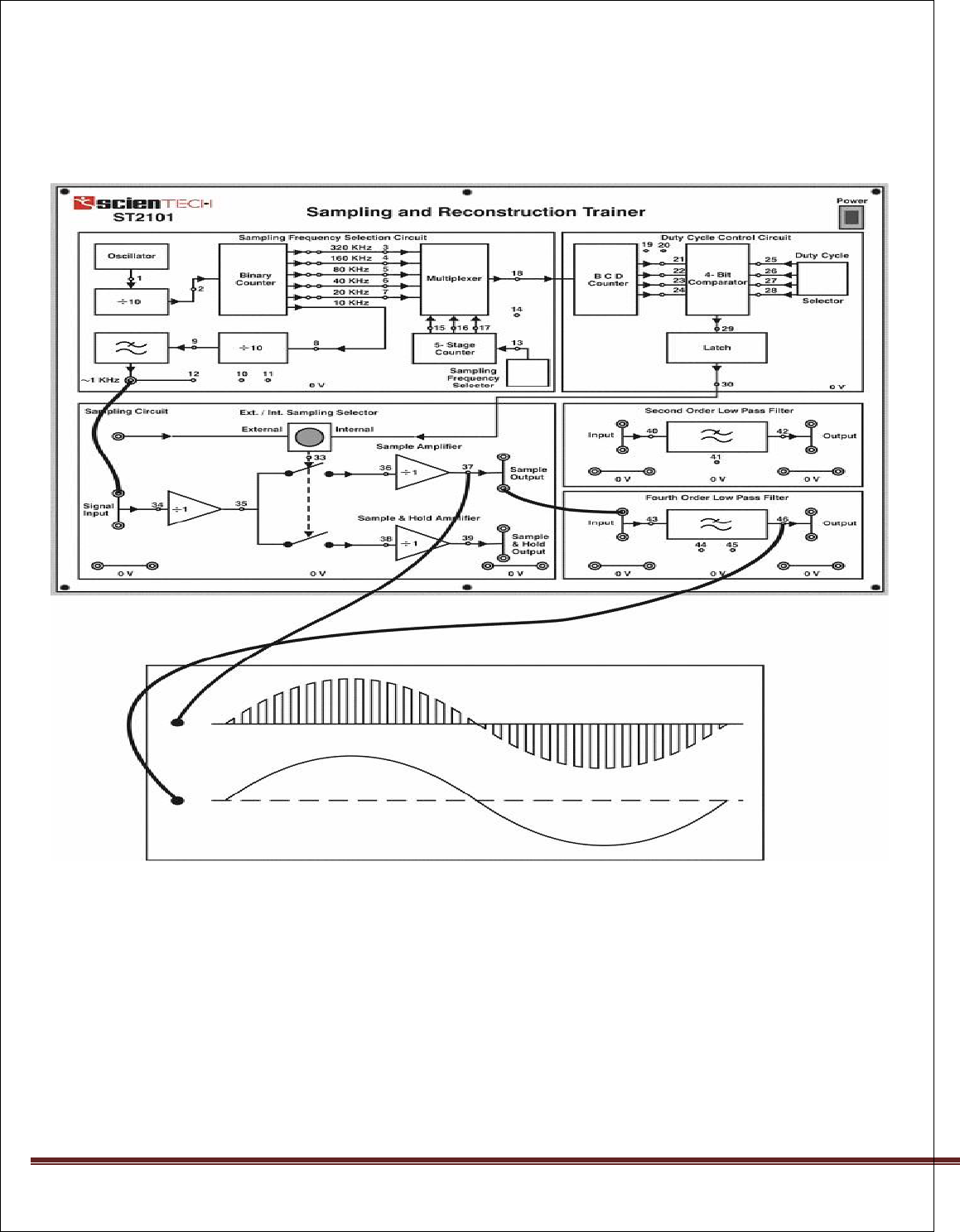
CIRCUIT DIAGRAM:-
LAKSHMI NARAIN COLLEGE OF TECHNOLOGY, BHOPAL
Department of Electronics and Communication Engineering Page 10
SIGNALRECONSTRUCTION:-

LAKSHMI NARAIN COLLEGE OF TECHNOLOGY, BHOPAL
Department of Electronics and Communication Engineering Page 11
PROCEDURE:-
A.
Setup for Sampling and reconstruction of signal .Initial setup of trainer :Duty cycle selector switch
position:Position5.
B Sampling selector switch :Internal position.
1. Connect the power cord to the trainer .Keep the power switch in ‘Off’ position.
2. Connect1 KHz Sine wave to signal Input.
3. Switch ‘ON’ the trainer's power supply and Oscilloscope.
4. Connect BNC connector to the CRO and to the trainer’s output port.
5. Select 320 KHz (Sampling frequency is1/10
th
of the frequency indicated by the illuminated LED)
sampling rate with the help of sampling frequency selector switch .
6. Observe 1 KHz sine wave and Sampled Output on Oscilloscope . Connect the Sampled output to
Input of Second Order and Fourth Order low pass Filter one after the other and observe the effect of
filtering on reconstructed output with help of oscilloscope. The display shows the reconstructed
original1KHz sine wave.
7. By successive presses of sampling Frequency Selector switch, change the sampling frequency to
2KHz, 4KHz, 8KHz, 16KHz (Sampling frequency is 1/10th of the frequency indicated by the
illuminated LED).Observe how SAMPLED output changes in each cases and how the lower
sampling frequencies introduce distortion into the filter’s output waveform. This is due to the fact
that the filter does not attenuate the unwanted frequency component significantly. Use of higher order
filter would improve the output waveform.
8. 1 KHz Sine wave being sampled at 32 KHz , so there are 32 samples for every cycle of the sine
wave,
Reconstruction of Analog Signal
9 Decrease the sampling rate from 32 KHz to 2 KHz. Observe the distorted waveform at filter's output.
This is due to the fact that sampling rate is kept very critical amount equal to Nyquist rate This is due
to the fact that the filter does not attenuate the unwanted frequency component significantly. Use of
higher order filter would improve the output waveform somewhat but recovered output is same as
that of original analog signal at moderate and higher sampling rates.

LAKSHMI NARAIN COLLEGE OF TECHNOLOGY, BHOPAL
Department of Electronics and Communication Engineering Page 12
OBSERVATION TABLE:
Parameters of Analog Signal ( v
m
and f
m
) :-
Sl.
No.
Theoretical
Sampling Rate
Observed
Sampling Rate
Percentage
Error
Recovered
Output
Voltage
RESULT:
Percentage Error between Theoretical Sampling Rate and Observed Sampling Rate is in permissible limits
And message is recovered properly.
QUESTIONS :
1. What is the significance of Sampling process.
2. State NY Quist Rate.
3. Describe Aliasing effect.
4. Name the circuit which performs Sampling.
5. Discuss the types of Practical Sampling.
6. Give the purpose of Sample and hold circuit.
LAKSHMI NARAIN COLLEGE OF TECHNOLOGY, BHOPAL
Department of Electronics and Communication Engineering Page 13
Date of Experiment: _______________
EXPERIMENT NO: 2
AIM:
To observe and analyze Time Division Multiplexed signal and to recover original analog signals from
multiplexed form.
APPARATUS USED:
1.TDM Trainer ,Kit
2. C.R.O and Connecting probes.
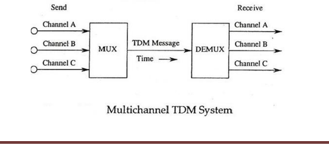
THEORY:
An important feature of pulse-amplitude modulation is a conservation of time. That is, for
a given message signal, transmission of the associated PAM wave engages the communication
channel for only a fraction of the sampling interval on a periodic basis. Hence, some of the time
interval between adjacent pulses of the PAM wave is cleared for use by the other independent
message signals on a time-shared basis. By so doing, a time-division multiplexed signal is
obtained (TDM), which enables the joint utilization of a common channel by a plurality of
independent message signals without mutual interference. Each input message signal is first
restricted in bandwidth by a low-pass pre-alias filter to remove the frequencies that are
nonessential to an adequate signal representation.
BLOCKDIAGRAM:

LAKSHMI NARAIN COLLEGE OF TECHNOLOGY, BHOPAL
Department of Electronics and Communication Engineering Page 14
PROCEDURE:
MULTIPLEXER:
1. Observe the AFgenerator-1 output and note down the amplitude and frequency.
2. Observe the AFgenerator-2 output and note down the amplitude and frequency.
3. Observe the AFgenerator-3 output and note down the amplitude and frequency.
4. Connect the AFgenerator1, 2 and 3outputs to CH1,CH2 and CH3inputs of TDM multiplexer.
5. Observe the TDM output over the screen of cathode ray oscilloscope.
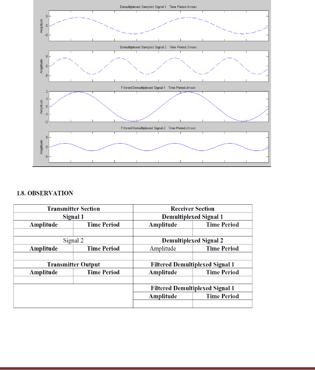
DEMULTIPLEXER:
1. Using probes connect the TDM multiplexers output to the TDM de-multiplexers input.
2. Connect the clock generator output, synchronizing pulse output of the transmitter trainer
to the respective inputs of the TDM de- multiplexer.
3. Observe the de-multiplexed signals which are the outputs to low passfilteratCH.1, CH.2 and
CH.3.
4. Note down the recovered output AMPLITUDE and FREQUENCY amounts.
LAKSHMI NARAIN COLLEGE OF TECHNOLOGY, BHOPAL
Department of Electronics and Communication Engineering Page 15
WAVEFORMS:
LAKSHMI NARAIN COLLEGE OF TECHNOLOGY, BHOPAL
Department of Electronics and Communication Engineering Page 16

LAKSHMI NARAIN COLLEGE OF TECHNOLOGY, BHOPAL
Department of Electronics and Communication Engineering Page 17
RESULT:
Time Division Multiplexing System signal has been observed and analyzed , Demultiplexed
signal is verified successfully.
QUESTIONS :
1. What is meant by multiplexing technique and what are the different types of Multiplexers?
2. Briefly explain about TDM and FDM?
3. What is the transmission bandwidth of a PAM/TDM signal?
4. Define crosstalk effect in PAM/TDM system?
5. What are the advantages of TDM system?
6. What are major differences between TDM and FDM?
7. Give the value of Ts in TDM system?
8. What care the applications of TDM system and give some example?
9. What is meant by signal overlapping?
10. Which type of modulation technique will be used in TDM?

LAKSHMI NARAIN COLLEGE OF TECHNOLOGY, BHOPAL
Department of Electronics and Communication Engineering Page 18
EXPERIMENT NO: 3
AIM:
To analyze a PCM system and interpret the modulated and demodulated waveforms for a
sampling frequency of 4 KHz.
APPARATUS:
1. PCM modulator trainer
2. PCM Demodulator trainer
3. C.R.O(30MHz)
4. Patch chords.
THEORY:
In Pulse code modulation (PCM) only certain discrete values are allowed for the
modulating signals. The modulating signal is sampled, as in other forms of pulse modulation.
But any sample falling within a specified range of values is assigned a discrete value. Each value
is assigned a pattern of pulses and the signal transmitted by means of this code. The electronic
circuit that produces the coded pulse train from the modulating waveform is termed a coder or
encoder. A suitable decoder must be used at the receiver in order to extract the original
information from the transmitted pulse train.
This PCM system consists of
PCM Modulator
1. Regulated power supply
2. Audio Frequency signal generator
3. Sample & Hold circuit
4. 8 Bit A/D Converter
5. 8 Bit Parallel-Serial Shift register
6. Clock generator/Timing circuit
7. DC source
PCM Demodulator
1. Regulated power supply
2. 8 Bit Serial-Parallel to shift register
3. 8 Bit D/A converter
4. Clock generator
5. Timing circuit
6. Passive low pass filter
7. Audio amplifiers
LAKSHMI NARAIN COLLEGE OF TECHNOLOGY, BHOPAL
Department of Electronics and Communication Engineering Page 19
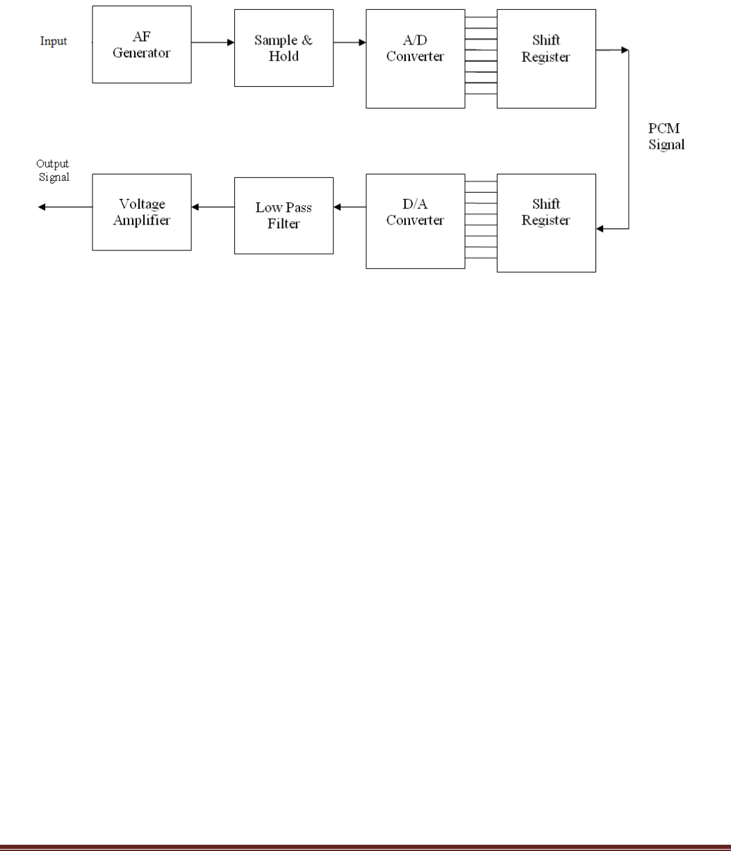
BLOCK DIAGRAM: PCM MODULATOR AND DEMODULATOR
PCM Operation:
The modulating signal is applied to sample & hold circuit. This applied signal will be super
imposed by +2.5V DC so that the negative portion the modulating signal will clamped to
positive, this process is needed, because input of the A/D Converter should be between 0 and
+5V. After level shifting is done the signal will be passed to sample &hold circuit. Sample
&hold circuit will sample the input signal during on period of the clock signal and will hold the
sampled output till next pulse comes. Sampling rate is 4KHz in this system.
So input of the A/D Converter is a stable voltage of certain level in between 0 and +5V.
A/D converter (encoder) will give a predetermined 8 bit code for the sampled input. This entire
conversion process will be made at a fast rate operating at high frequency clock i.e. 1MHz.
Coded output of the A/D converter is applied to input of the parallel in serial out register through
a latch. This shift register is operating at 64 KHz (sampling frequency is 4KHz, so to shift 8 bits
from parallel to serial we need 64KHz). This output (PCM) is transmitted through a co-axial
cable which represents a communication channel.
PCM signal from modulator (encoder) is applied to serial to parallel register. This shift
register is also operating at 64KHz clock at which parallel to serial shift register is operating at
PCM modulator (these both the clock signals should be in synchronized with each other in order
to get proper decoded output).So the output of the serial to parallel register is a 8 bit code .This 8
bit code is applied to 8 bit D/A converter. Output of the D/A converter will be a staircase
signaling between 0 and +5V. This stair case signal is applied a low pass filter. This low pass
will smoothen the staircase signal so that we will get a recovered AF signal. We can use a
voltage amplifier at the output of the low pass filter to amplify there covered AF signal to desired
voltage level.

LAKSHMI NARAIN COLLEGE OF TECHNOLOGY, BHOPAL
Department of Electronics and Communication Engineering Page 20
PROCEDURE:
PCM Operation (with AC input):
Modulation:
1. Connect AC signal of 2 V
pp
amplitude to Sample and Hold circuit.
2. Keep the CRO in dual mode. Connect one channel to the AF signal and another channel to
the Sample and Hold output. Observe and sketch the sample and hold output.
3. Connect the Sample and Hold output to the A/D converter and observe the PCM output using
Storage oscilloscope.
4. Observe PCM output by varying AF signal voltage.
Demodulation:
1. Connect PCM signal to the demodulator input (S-P shift register) from the PCM modulator
with the help of coaxial cable (supplied with the trainer).
2. Connect clock signal (64 KHz) from the transmitter to the receiver using coaxial cable.
3. Connect transmitter clock to the timing circuit.
4. Keep CRO in dual mode. Connect CH1 input to the sample and hold output and CH2 input to
the D/A converter output .
5. Observe and sketch the D/A output.
6. Connect D/A output to the LPF input.
7. Observe the output of the LPF/Amplifier and compare it with the original modulating signal .
8. From above observation you can verify that there is no loss in information (modulating
signal) in conversion and transmission process.
9. Disconnect clock from transmitter and connect to local oscillator (i.e., Clock generator
output) with remaining setup as it is.
Observe D/A output and compare it with the previous result. This signal is little bit distorted in shape. This is because
lack of synchronization between clock at transmitter and clock at receiver
LAKSHMI NARAIN COLLEGE OF TECHNOLOGY, BHOPAL
Department of Electronics and Communication Engineering Page 21
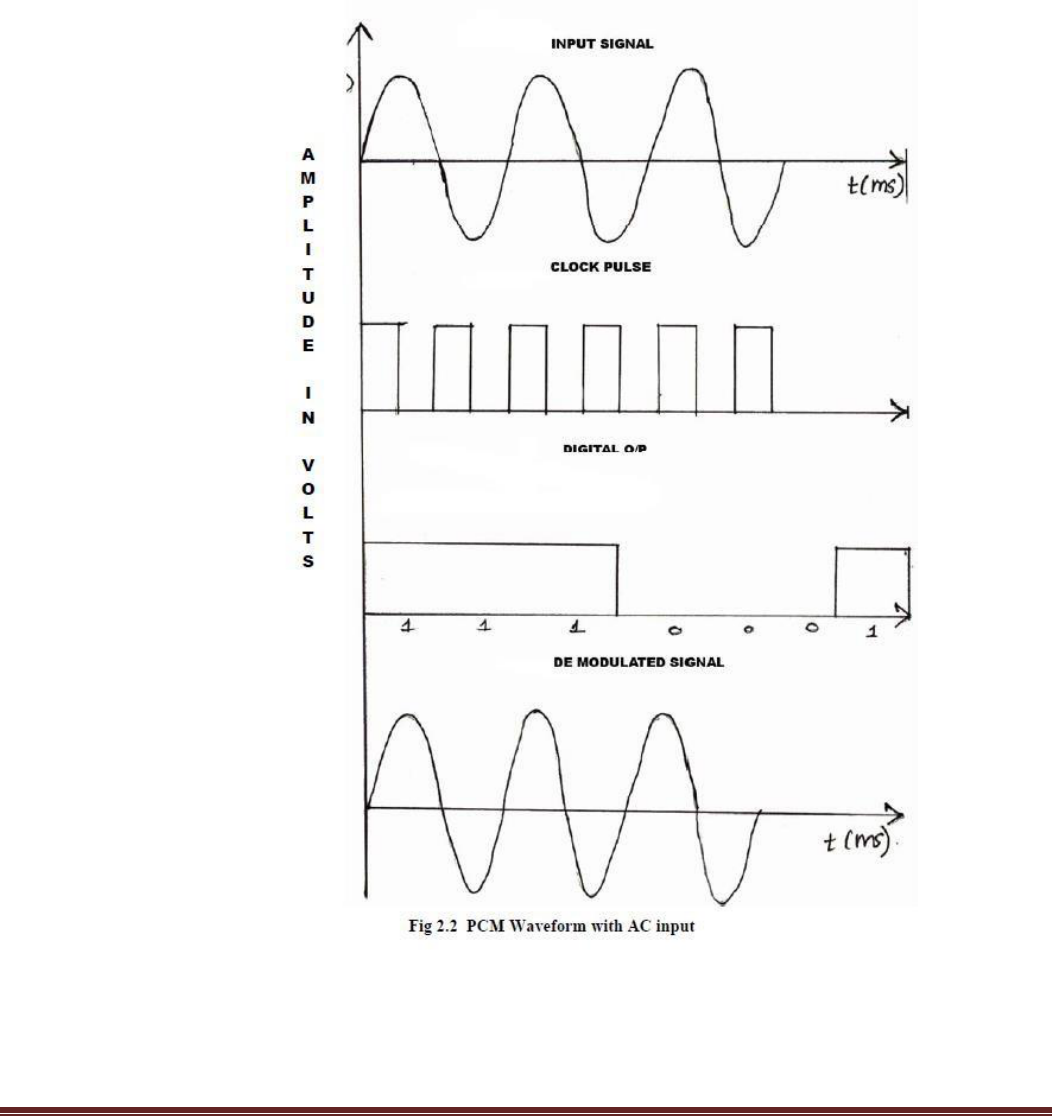
EXPECTEDWAVEFORMS:

LAKSHMI NARAIN COLLEGE OF TECHNOLOGY, BHOPAL
Department of Electronics and Communication Engineering Page 22
Analog Signal input
Sample and hold circuit
Clock signal
Clock signal
PCM Output
D/A converter output signal
LPF output signal
Demodulated output
OBSERVATIONS:
PCM Modulation with AC input
AMPLITUDE FREQUENCY
RESULT:
Binary output of Pulse Code modulator has been observed and analog message is recovered at PCM
demodulator and graphs were plotted.
VIVA QUESTIONS:
1. What do you mean by quantizing process?
2. What will happen when sampling rate is greater than Nyquist rate?
3. What will happen when sampling rate is less than Nyquist rate?
4. Find the A/D Converter output for input DC voltage of 3.6V.
5. Mention some applications of PCM.
6. What is the function of Sample and Hold circuit?
LAKSHMI NARAIN COLLEGE OF TECHNOLOGY, BHOPAL
Department of Electronics and Communication Engineering Page 23
Date of Experiment:_______________
EXPERIMENT NO: 4
AIM:
To analyze a Delta modulation system. and interpret the modulated and demodulated waveforms
APPARATUS:
1. DM Modulator and Demodulator trainer-
2. C.R.O(30MHz)
3. Patch chords.
BLOCK DIAGRAM: DELTA MODULATOR AND DEMODULATOR
LAKSHMI NARAIN COLLEGE OF TECHNOLOGY, BHOPAL
Department of Electronics and Communication Engineering Page 24
THEORY:
Delta Modulation is a form of pulse modulation where a sample value is represented as a single
bit. This is almost similar to differential PCM, as the transmitted bit is only one per sample justto
indicate whether the present sample is larger or smaller than the previous one. The encoding,
decoding and quantizing process become extremely simple but this system cannot handle rapidly
varying samples. This increases the quantizing noise.
The trainer is a self sustained and well organized kit for the demonstration of delta modulation
and demodulation .The system consist of :
DM Modulator trainer kit
1. Regulated power supply
2. Audio Frequency signal generator
3. Buffer/signal shaping network
4. Voltage comparator
5. 4 Bit UP/DOWN counter
6. Clock generator/Timing circuit
7. 4 Bit D/A converter
8. DC source
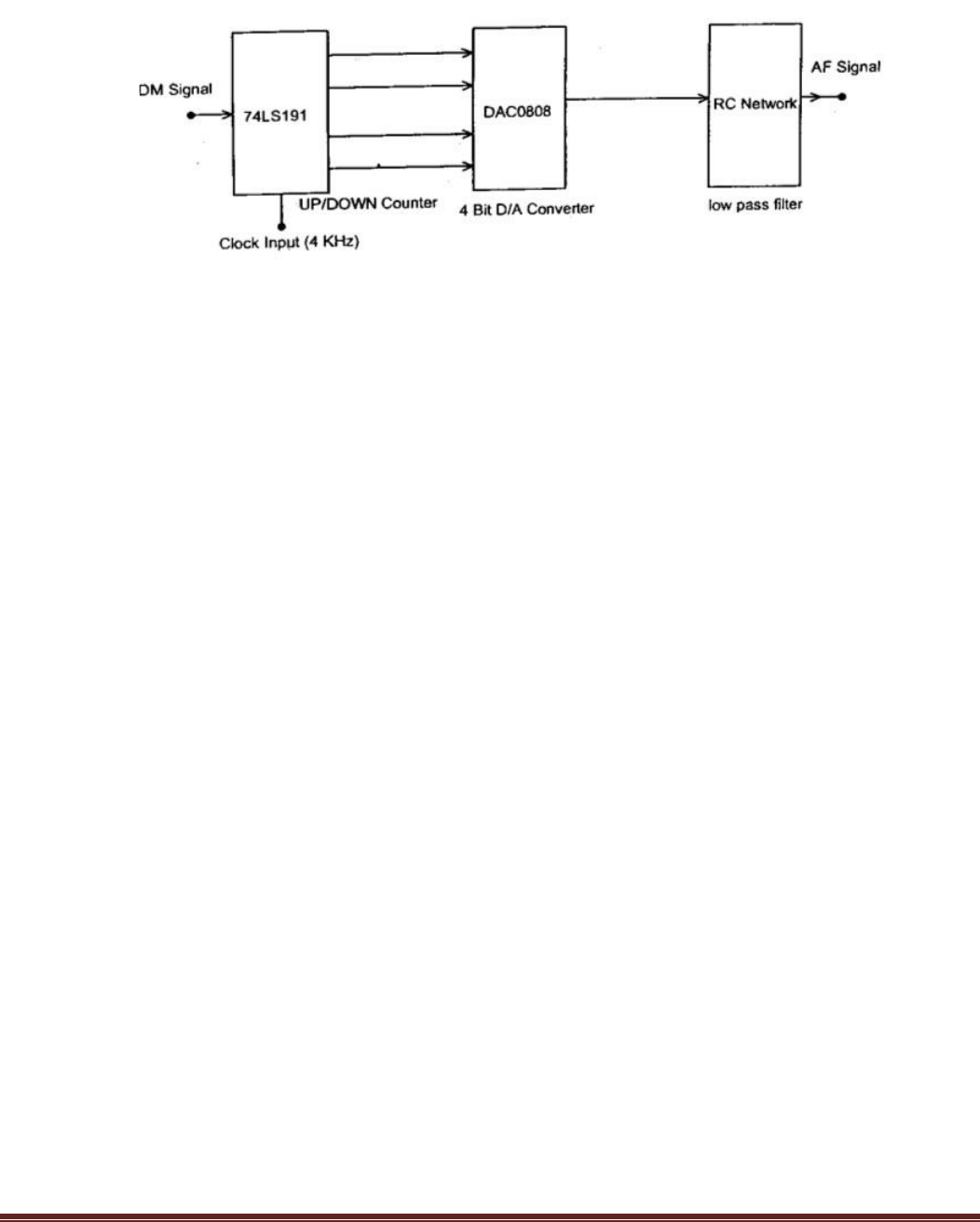
DM Demodulator trainer kit
1. Regulated power supply
2. 4 Bit UP/DOWN counter
3. 4 Bit D/A converter
4. Clock generator
5. Passive low pass filter
6. Audio amplifier
Regulated power supply:
This consists of a bridge rectifier followed by Capacitor filters and three terminal regulators 7805
and 7905 to provide regulated DC voltages of +-5V and +12V@ 300Ma each to the on board
circuits. These supplies have been internally connected to the circuits. so no external connections
are required for operation.
Audio Frequency (AF) signal generator

LAKSHMI NARAIN COLLEGE OF TECHNOLOGY, BHOPAL
Department of Electronics and Communication Engineering Page 25
Sine wave signal of 250Hz, 500 Hz, 1kHz and 2KHz is generated to use as a modulating
(message or information) signal to be transmitted. This is an Op-Amp based Wien bridge
Oscillators is a FET. input general purpose Operational Amplifier .Amplitude control is provided
in the circuit to vary the output amplitude of AF signal.
Clock generator/Timing circuit:
A TTL compatible clock signal of 4 KHz frequency is provided on board to use as a clock to the
various circuits in the system. This circuit is astable multi vibrator using 555 timer followed by
a buffer.
Voltage comparator:
This circuit is build with IC LM339 The LM339 series consists of four independent precision
voltage comparators with an offset voltage specification as low as 2mV for all four comparators.
These were designed specifically to operate from a single power supply over a wide range of
voltages .Operation from split power supplies is also possible and the low power supply current
drain is independent of the magnitude of the power supply voltage. These comparators also have
a unique characteristic in that the common mode voltage range includes ground, even though
operated from a single power supply voltage. Application areas include limit comparators simple
analog to digital converters: pulse, square and time delay generators. wide range VCO;MOS
clock timers; multi vibrators and high voltage digital logic gates .The LM139 series was
designed to directly interface with TTL and CMOS. When operated from both plus and minus
power supplies, they will directly interface with MOS logic where the low power drain of the
LM339 is a distinct advantage over standard comparators .For circuit connections and other
operating conditions.
Sample and Hold Circuit
It is a Bi stable multi vibrator or a clocked D flip flop so as to store the output of comparator for
one clock duration.
Uni polar to Polar Converter
The purpose of this converter is to convert Low bit zero voltage amounts into a specific negative
amounts so that when applied to the integrator, negative saw tooth patterns are also produced.
Integrator or Low pass filter
This is a series of simple RC networks provided on receiver board to smoothen the output of the
D/A converter output. RC values are chosen such that the cutoff frequency would be at 100 Hz.
Also the purpose of Integrator of transmitter feedback path is to convert pulses in the form of
Saw tooth signal.

LAKSHMI NARAIN COLLEGE OF TECHNOLOGY, BHOPAL
Department of Electronics and Communication Engineering Page 26
PROCEDURE:
DM Modulator:
1. Study the theory of operation
2. Connect the trainer-
3. Observe the output of Audio Frequency generator using CRO; it should be a Sine wave of
1000 Hz frequency with 3Vpp amplitude.
4. Observe the output of the clock generator it should be 4 KHz frequency of square wave with 5
V
pp
amplitude.
5. Observe and plot the signals at D/A converter output (i.e. non-inverting input of the
comparator), DM signal using CRO and compare them with the waveforms given in figure.
6. Connect DM signal to the DM input of the demodulator.
7. Connect clock (4 KHz) from modulator to the clock input of the demodulator Connect clock
input of UP/DOWN counter to the clock from transmitter with the help of springs provided.
8. Observe digital output (LED indication) of the UP/DOWN counter and compare it with the
output of the UP/DOWN. By this both the outputs are same noticed.
9. Observe and plot the output of the D/A converter and compare it with the waveforms given
in figure.
10. Measure the demodulated signal (i.e. output of the D/A converter with the help of multi
meter and compare it with the original signal. From the above observation it is noticed that both
the voltages are equal and there is no loss in process of modulation ,transmission and
demodulation.
11. Similarly the DM operation can be verified for different values of modulating signal.
Observe and sketch the D/A output.
12. Connect D/A output to the LPF input.
13. Observe the output of the LPF/Amplifier and compare it with the original modulating signal .
14. From the above observation you can verify that there is no loss in information in conversion
and transmission process.
15. Disconnect clock from transmitter and connect to local oscillator (i.e. clock generator output
with remaining setup as it is. Observe demodulated signal output and compare it with the
previous result. This signal is little bit distorted in shape. This is because lack of synchronization
between clock at transmitter and clock at receiver.
16. Observe and plot the signals at D/A converter output (i.e. non-inverting input of the
comparator), DM signal using CRO and compare them with the waveforms given in figure.
17. Similarly the DM operation can be verified for different values of modulating signal.
LAKSHMI NARAIN COLLEGE OF TECHNOLOGY, BHOPAL
Department of Electronics and Communication Engineering Page 27
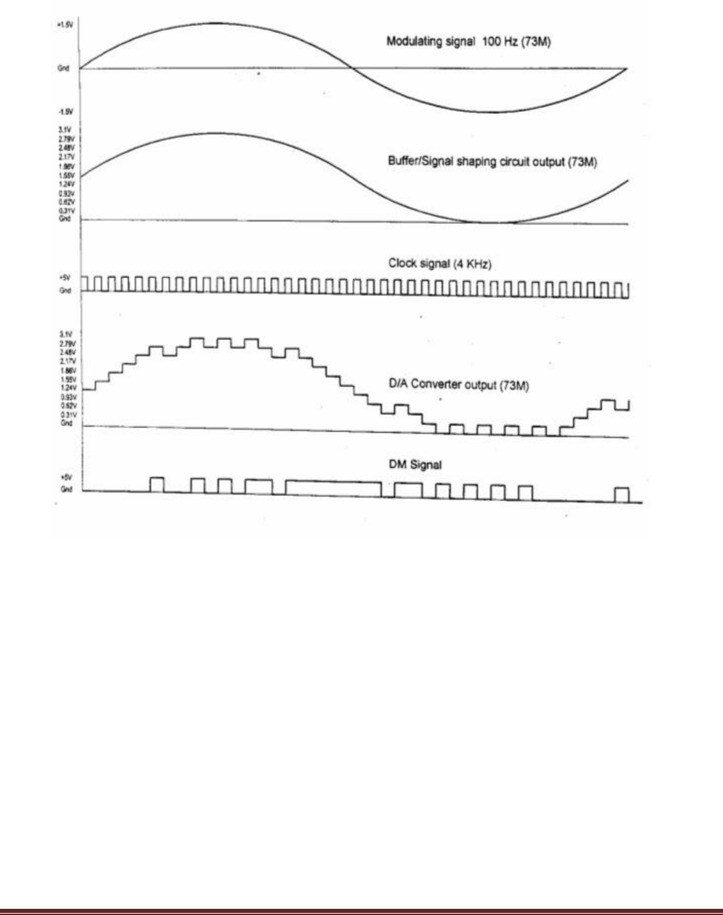
EXPECTED WAVEFORMS FOR AC INPUT

LAKSHMI NARAIN COLLEGE OF TECHNOLOGY, BHOPAL
Department of Electronics and Communication Engineering Page 28
OBSERVATION TABLE
SLNO.
SIGNALS AT VARIOUS STAGES
AMPLITUDE
FREQUENCY
ANALOG INPUT SIGNAL
INTEGRATORS OUTPUT
CLOCK SIGNAL
DM TRANSMITTER OUTPUT
DM RECIVERS INPUT
DM RECIVERS OUTPUT
RESULT:
Thus the Delta modulation and demodulation is performed and waveforms with
readings are plotted and observed.
VIVAQUESTIONS:
1. Compare DPCM, PCM and Delta modulation.
2. How to reduce the quantization noise that occurs in DM?
3. A band pass signal has a spectral range that extends from 20 to 82 KHz. Find the acceptable
sampling frequency.
4. Find the bit rate for a message when clock rate is kept 64 kHz
5. Mention the drawbacks of DM.
LAKSHMI NARAIN COLLEGE OF TECHNOLOGY, BHOPAL
Department of Electronics and Communication Engineering Page 29
Date of Experiment:_______________
EXPERIMENT NO: 5
AIM:
To analyze a FSK modulation system and interpret the modulated and demodulated waveforms
APPRATUS:
1. FSK Trainer Kit- Scientech
2. Dual Trace oscilloscope
3. Digital Multi meter
4. C.R.O (30MHz)
5. Patch chords.
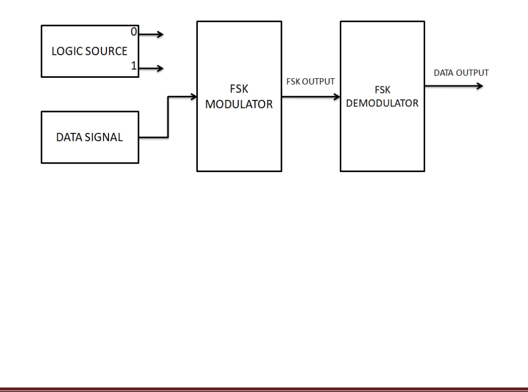
BLOCKDIAGRAM OF FSK SYSTEM
THEORY:
In Frequency shift keying, the carrier frequency is shifted (i.e. from one frequency to another)
corresponding to the digital modulating signal. If the higher frequency is used to represent a data
‘1’ & lower frequency a data ‘0’, the resulting FSK waveform appears.
Thus

LAKSHMI NARAIN COLLEGE OF TECHNOLOGY, BHOPAL
Department of Electronics and Communication Engineering Page 30
Data=1 High Frequency
Data=0 Low Frequency
It is also represented as a sum of two ASK signals. The two carriers have different frequencies and the
digital data is inverted .The demodulation of FSK can be carried out by a PLL. As known the PLL tries to
‘lock’ the input frequency. It achieves this by generating corresponding output voltage to be fed to the
VCO, if any frequency deviation at its input is encountered. Thus the PLL detector follows the frequency
changes and generates proportional output voltage. The output voltage from PLL contains the carrier
components. Therefore to remove this, the signal is passed through Low Pass Filter. The resulting wave is
too rounded to be used for digital data processing. Also, the amplitude level may be low due to
attenuation
PROCEDURE:
1. Connect the trainer kit to the mains and switch ON the power supply.
2. Check internal RPS voltage (it should be 12V) and logic source voltage for logic one (it
should be 12V)
3. Observe the data signal using oscilloscope. Observe the various data signals (2KHZ,4KHZ, 8 KHZ
and 16KHZ) using CRO
4. Note down the parameters of Data. (Amplitude and Time Period). Time period has to match
with the selected Data rate.
5. Connect the output of the logic source to data input of the FSK modulator.
6. Check the frequencies and amplitudes of the provided carrier signals.
7. See the carrier frequency of the FSK modulator as 1.2 KHz using control F0 (this represents
logic 0). Then set another frequency as 2.4 KHz using control F1 (this represents logic 1)
8. Connect the data input of the FSK modulator to the output of the data signal generator.
Observe the signal that comes out of FSK modulator and note down the readings.
9. Connect the FSK modulator output to the input of the FSK demodulator. Observe the
waveform of FSK demodulator output using CRO and note down the readings
OBSERVATIONS:
TYPE OF SIGNAL
AMPLITUDE
FREQUENCY
BINARY DATA
CARRIER SIGNAL (S1)
CARRIER SIGNAL (S2)
MODULATED SIGNAL
MODULATED SIGNAL
RECOVERED BINARY DATA
( DEMODULATED SIGNAL )

LAKSHMI NARAIN COLLEGE OF TECHNOLOGY, BHOPAL
Department of Electronics and Communication Engineering Page 31
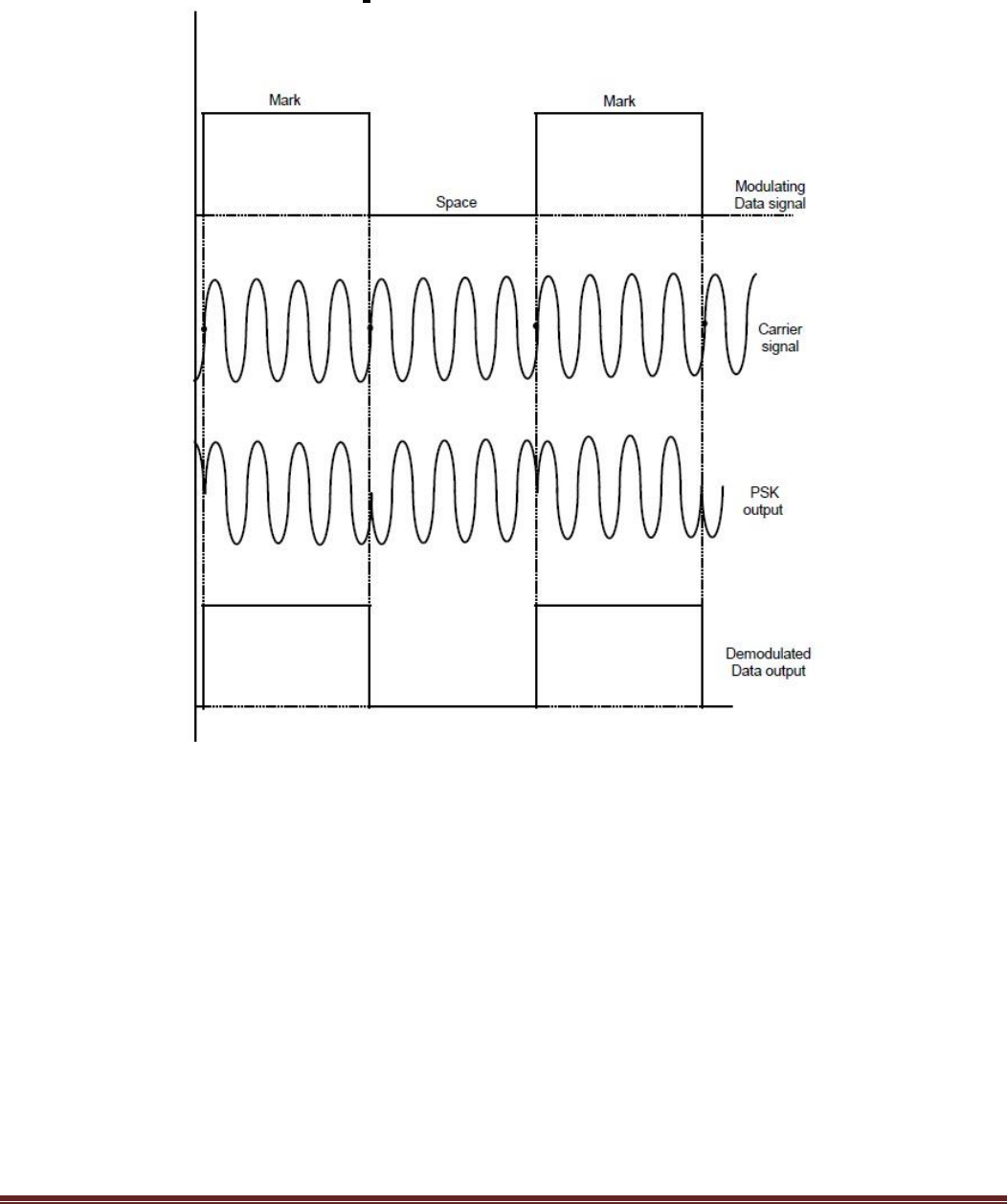
EXPECTED WAVEFORM:
RESULT:
Waveforms of FSK modulated and demodulated signal has been observed and readings are taken and
analyzed properly
VIVA QUESTIONS:
1. What are the advantages of FSK over ASK and PSK?
2. Forthegiven8bitdata10111010drawtheFSKoutputwaveform.
3. Draw the constellation diagram of FSK.
4. What is the consumed Bandwidth of FSK?
5. Give the block diagrams of COHERENT FSK Modulator and Demodulator.
LAKSHMI NARAIN COLLEGE OF TECHNOLOGY, BHOPAL
Department of Electronics and Communication Engineering Page 32
PSK Modulator
PSK
Demodulator
Date of Experiment:_______________
EXPERIMENT NO: 6
AIM:
To analyze a PSK modulation system and interpret the modulated and demodulated waveforms.
APPRATUS:
1. BPSK Trainer Kit - Scientech
2. Dual Trace oscilloscope
3. Digital Multi meter
4. C.R.O (30MHz)
5. Patch chords.
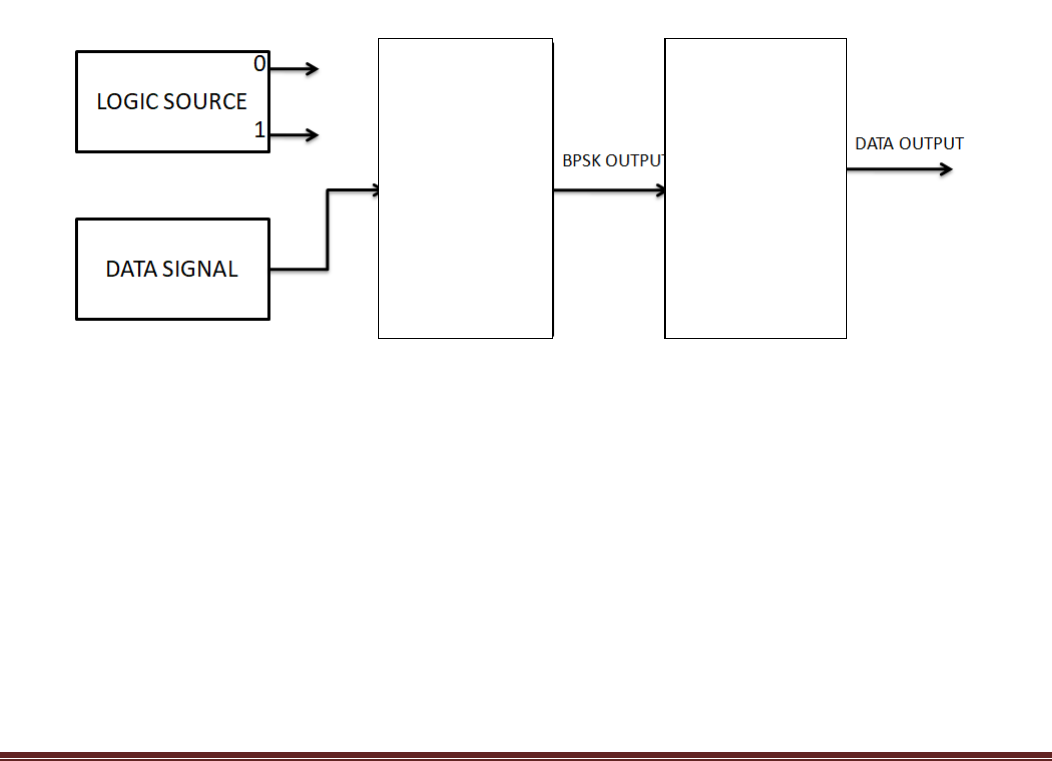
BLOCK DIAGRAM:
Theory:
Phase shift keying is a modulation/data transmitting technique in which phase of the carrier
signal is shifted between two distinct levels. In a simple PSK (ie binary PSK) un shifted carrier
V
c
cosω
c
t is transmitted to indicate a 1 condition, and the carrier shifted by 180
0
ie.( – V
c
cosω
c
t) is
transmitted to indicate as 0 condition.
.

LAKSHMI NARAIN COLLEGE OF TECHNOLOGY, BHOPAL
Department of Electronics and Communication Engineering Page 33
PROCEDURE:
1. Connect the trainer to mains and switch ON the power supply.
2. Measure the output of the regulated power supply ie. +5Vand -5Vwith the help of digital
multi meter.
3. Observe the output of the carrier generator using CRO,
4. Observe the various data signals (2KHZ,4KHZ,8 KHZ and 16KHZ)using CRO
5. Connect data signal say 4KHZ from data source to data input of the modulator.
6. Keep CRO in dual mode and connect CH1 input of the CRO to data signal and CH2 to the
output of the PSK modulator.
7. Observe the PSK output signal with respect to data signal and plot the waveforms.
8. Connect the PSK output to the PSK input of the demodulator.
9. Observe carrier to the carrier input of the PSK demodulator.
10. Keep CRO in dual mode and connect CH1 to data signal (at modulator) and CH2 to the
output of the demodulator.
11. Compare the demodulated signal with the original signal. It is noticec that there is no loss in
modulation and demodulation process
12. Repeat the steps 6 to12 with different data signals .
LAKSHMI NARAIN COLLEGE OF TECHNOLOGY, BHOPAL
Department of Electronics and Communication Engineering Page 34
EXPECTED WAVEFORMS:
LAKSHMI NARAIN COLLEGE OF TECHNOLOGY, BHOPAL
Department of Electronics and Communication Engineering Page 35
OBSERVATIONS:
TYPE OF SIGNAL
AMPLITUDE
FREQUENCY
BINARY DATA-2KHz (Theoretical Rate
)
BINARY DATA - 4 KHz (Theoretical Rate )
BINARY DATA - 8 KHz (Theoretical Rate )
CARRIER SIGNAL
MODULATED SIGNAL
RECOVERED BINARY DATA
( DEMODULATED SIGNAL )
RESULT:
Waveforms of PSK modulated and demodulated signal has been observed and readings are taken and
analyzed properly
VIVAQUESTIONS:
1. What are the advantages of PSK over ASK and FSK?
2. For the given 8bit data 10111010 draw the PSK output waveform.
3. Draw the constellation diagram of PSK.
4. What is the consumed Bandwidth of PSK?
5. Give the block diagrams of NON COHERENT PSK Modulator and Demodulator.

LAKSHMI NARAIN COLLEGE OF TECHNOLOGY, BHOPAL
Department of Electronics and Communication Engineering Page 36
Date of Experiment:_______________
EXPERIMENT NO: 7
AIM:
To analyze a ASK modulation system and interpret the modulated and demodulated waveforms.
APPRATUS:
1. ASK Trainer Kit-Scientech
2. Dual Trace oscilloscope
3. Digital Multi meter
4. C.R.O (30MHz)
5 Patch chords.
THEORY:
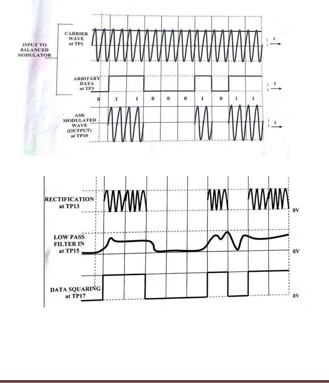
ASK modulation involves the variation of the amplitude of the carrier waves in accordance with
the data stream. The simplest method of modulating a carrier with a data stream is to change the
amplitude of the carrier wave every time the data changes. This modulation technique is known
as amplitude shift keying. The simplest way of achieving amplitude shift keying is ‘ON’ the
carrier whenever the data bit is ‘HIGH’ & switching ‘OFF’ when the data bit is low i.e. the
transmitter outputs the carrier for HIGH & totally suppresses the carrier for low. This technique
is known as ON-OFF keying Fig. illustrates the amplitude shift keying forthe given data stream.
Thus, DATA= HIGH (CARRIER TRANSMITTED)DATA = LOW (CARRIER SUPPRESSED
) .The ASK waveform is generated by a balanced modulator circuit, also known as a linear
multiplier, As the name suggests, the device multiplies the instantaneous signal at its two inputs,
the output voltage being product of the two input voltages at any instance of time. One of the
inputs is a/c coupled ‘carrier’ wave of high frequency. Generally the carrier wave is a sine wave
since any other waveform would increase the bandwidth imparting any advantages requirement
without improving or to it. The other i/p which is the information signal to be transmitted, is
D.C. coupled. It is known as modulating signal
In order to generate ASK waveform it is necessary to apply a sine wave at carrier input &
the digital stream at modulation input. The double balanced modulator is shown in fig.
LAKSHMI NARAIN COLLEGE OF TECHNOLOGY, BHOPAL
Department of Electronics and Communication Engineering Page 37
RF SIGNAL
ASK
MODULATOR
ASK
DEMODULATOR
DATA/CLOCK
GENERATOR
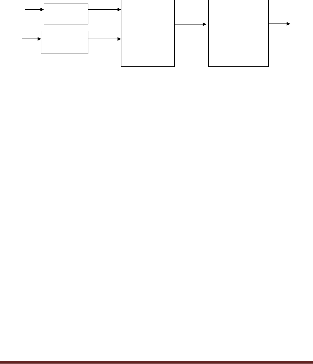
BLOCK DIAGRAM:
The data stream applied is uniploar i.e. 0 Volt at logic LOW & +5Volts at logic HIGH. The
output of balanced modulator is a sine wave, unchanged in phase when a data bit ‘HIGH’ is
applied to it. In this case the carrier is multiplied with a positive constant voltage when the data
bit LOW is applied , the carrier is multiplied by0 Volts, giving rise to 0Volt signal at modulator’s
o/p. The ASK modulation results in a great simplicity at the receiver. The method to demodulate
the ASK waveformis to rectify it, pass it filter &’square up’the resulting waveform. The output
is the original digital data stream. Fig. shows the functional blocks required in order to
demodulate the ASK waveform at receiver
PROCEDURE:
Modulation:
1. Connect the sine wave carrier generator to the carrier input of the modulator.
2. And also connect data clock D1 i.e., modulating signal to the modulation input
3. Switch ON the power supply.
4. Observe the modulated output.
5. By changing the data clocks D2,D3,D4 observe the output.
Demodulation:
1. Connect ASK output to the Product modulator input and observe the waveform.
2. Now connect Product modulator output to the low pass filter input and observe the output.
3. Connect LPF output to the Comparator circuit and observes the demodulated output
waveform.
4. By changing the different data clocks and observe the demodulation output.
LAKSHMI NARAIN COLLEGE OF TECHNOLOGY, BHOPAL
Department of Electronics and Communication Engineering Page 38
EXPECTEDWAVEFORMS:
LAKSHMI NARAIN COLLEGE OF TECHNOLOGY, BHOPAL
Department of Electronics and Communication Engineering Page 39
OBSERVATIONS:
TYPE OF SIGNAL
AMPLITUDE
FREQUENCY
BINARY DATA- 2KHz(Theoretical Rate
)
BINARY DATA - 4 KHz (Theoretical Rate )
BINARY DATA - 8 KHz (Theoretical Rate )
CARRIER SIGNAL
MODULATED SIGNAL
RECOVERED BINARY DATA
( DEMODULATED SIGNAL )
RESULT:
Thus the ASK modulation and demodulation were performed and wave forms were
observed along with the readings.
VIVA QUESTIONS:
1. What are the advantages of ASK over PSK and FSK?
2. For the given 8 bit data 10111010 draw the ASK output waveform.
3. Draw the constellation diagram of ASK.
4. What is the consumed Bandwidth of ASK?
5. Applications of ASK.
LAKSHMI NARAIN COLLEGE OF TECHNOLOGY, BHOPAL
Department of Electronics and Communication Engineering Page 40
Date of Experiment:_______________
EXPERIMENT NO: 8
AIM:
Observe the waveforms of differential phase shift keyed modulated signal and recover the binary data
APPRATUS:
1. DPSK Trainer Kit
2. Dual Trace oscilloscope
3. Digital Multi meter
4. C.R.O (30MHz)
5. Patch chords.
BLOCK DIAGRAM:
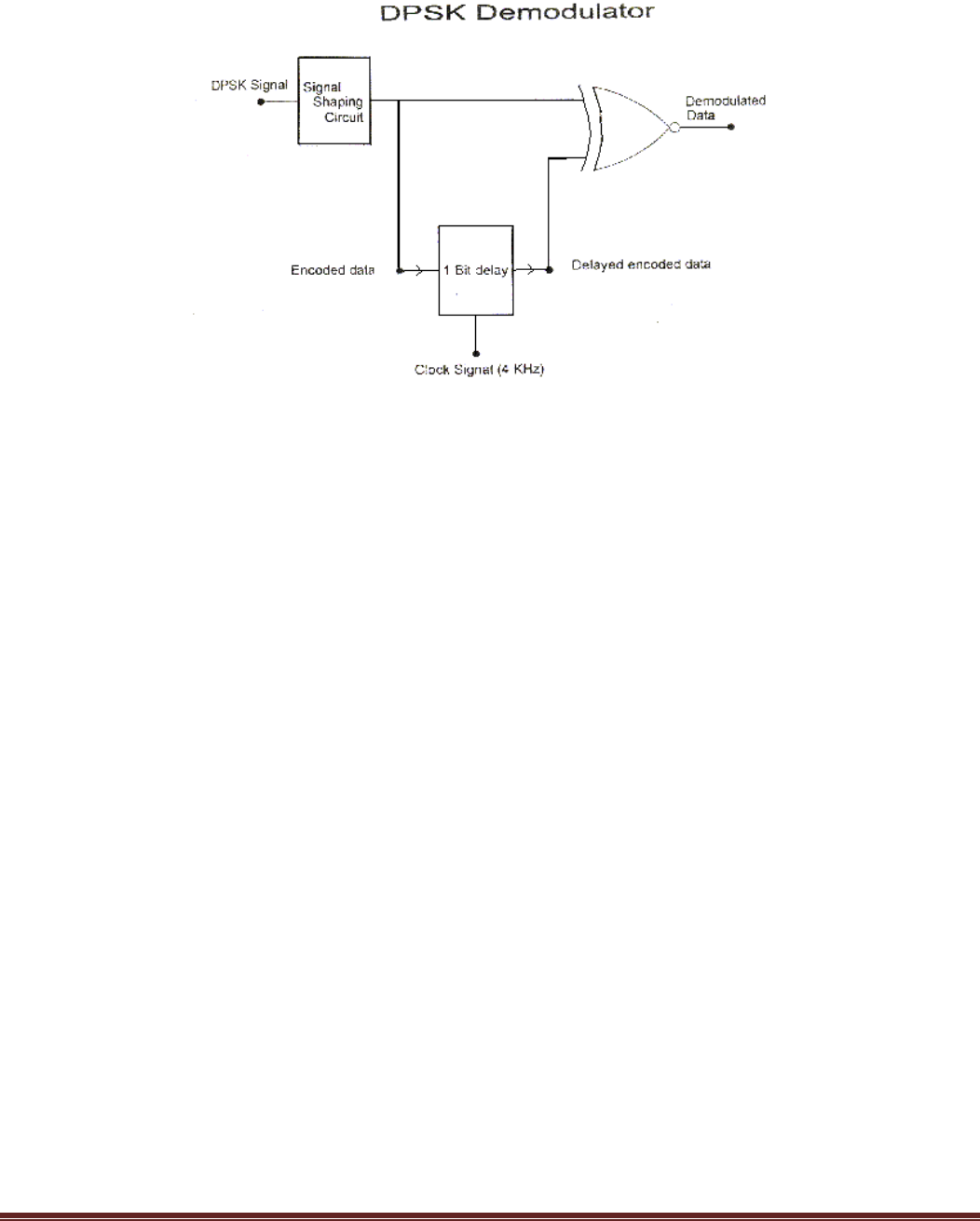
LAKSHMI NARAIN COLLEGE OF TECHNOLOGY, BHOPAL
Department of Electronics and Communication Engineering Page 41
THEORY:
DPSK: Phase Shift Keying requires a local oscillator at the receiver which is accurately
synchronized in phase with the un-modulated transmitted carrier, and in practice this can be
difficult to achieve. Differential Phase Shift Keying (DPSK) over comes the difficult by
combining two basic operations at the transmitter (1) differential encoding of the input binary
wave and (2) phase shift keying – hence the name differential phase shift keying. In other words
DPSK is a non-coherent version of the PSK.
The differential encoding operation performed by the modulator is explained below Let b (t) be
the binary message to be transmitted. An encoded message stream b(t) is generated from b’(t) by
using a logic circuit The first bit in b(t) is arbitrary which may be chosen as 1 or 0 . The
subsequent bits in b(t) are determined on the basis of the rule that when b’(t) is 1 b(t) does not
change its value. In the first bit stream ,the initial bit (arbitrary) is1 and in the second bit stream,
the initial bit is 0 EX-NOR gate can be used to perform this operation as its output is a 1 when
both the input are same, and a 0 when the inputs are different.
b’(t) 0 1 1 0 0
b(t) 1 0 0 0 1 0
Phase 0
0
180
0
180
0
180
0
0
0
180
0
B(t) 0 1 1 1 0 1
Phase 180
0
0
0
0
0
0
0
180
0
0
0

LAKSHMI NARAIN COLLEGE OF TECHNOLOGY, BHOPAL
Department of Electronics and Communication Engineering Page 42
Example for Complete DPSK operation (with arbitrary bit as 0):
Message signal (to be transmitted) 0 1 1 0 0
Encoded data (differential data) 0 1 1 1 0 1
Transmitted signal phase: 180
0
0
0
0
0
0
0
180
0
0
0
Received signal phase: 180
0
0
0
0
0
0
0
180
0
0
0
Encoded data (differential data) 0 1 1 1 0
Message signal (Demodulation) 0 1 1 0 0
DPSK Demodulator:
PROCEDURE:
MODULATOR
1. Connect carrier signal to carrier input of the PSK Modulator.
2. Connect data signal from data input of the X-NOR gate.
3. Keep CRO in dual mode.
4. Connect CH1input of the CRO to data signal and CH2 input to the encoded data (which is
nothing but the output of the X-NOR gate).
5. Observe the encoded data with respect to data input. The encoded data will be in a given
sequence.
6. Actual data signal: 10101101001010110100
7. Encoded data signal: 01100011011001110010
8. Now connect CH2 input of the CRO to the DPSK output and CH1 input to the encoded data.
Observe the input and output waveforms and plot the same.
9. Compare the plotted waveforms with the given waveforms in fig:1.3
DEMODULATOR:
1. Connect DPSK signal to the input of the Demodulator.
2. Keep CRO in dual mode. Connect CH1 input to the encoded data (at modulator) and CH2
input to the encoded data (at demodulator).
3. Observe and plot both the waveforms and compare it with the given waveforms. It willbe
noticed that both the signals are same with one bit delay.
4. Keep CRO in dual mode. Connect CH1 input to the data signal(at modulator) and CH2 input
LAKSHMI NARAIN COLLEGE OF TECHNOLOGY, BHOPAL
Department of Electronics and Communication Engineering Page 43
to the output of the demodulator.
5. Disconnect clock from transmitter and connect to local oscillator clock (i.e., clock generator
output from De Modulator) with remaining setup as it is. Observe demodulator output and
compare it with the previous output. This signal is little bit distorted. This is because lack of
synchronization between clock at modulator and clock at demodulator. We can get further
perfection in output waveform by adjusting the locally generated clock frequency by varying
potentiometer.
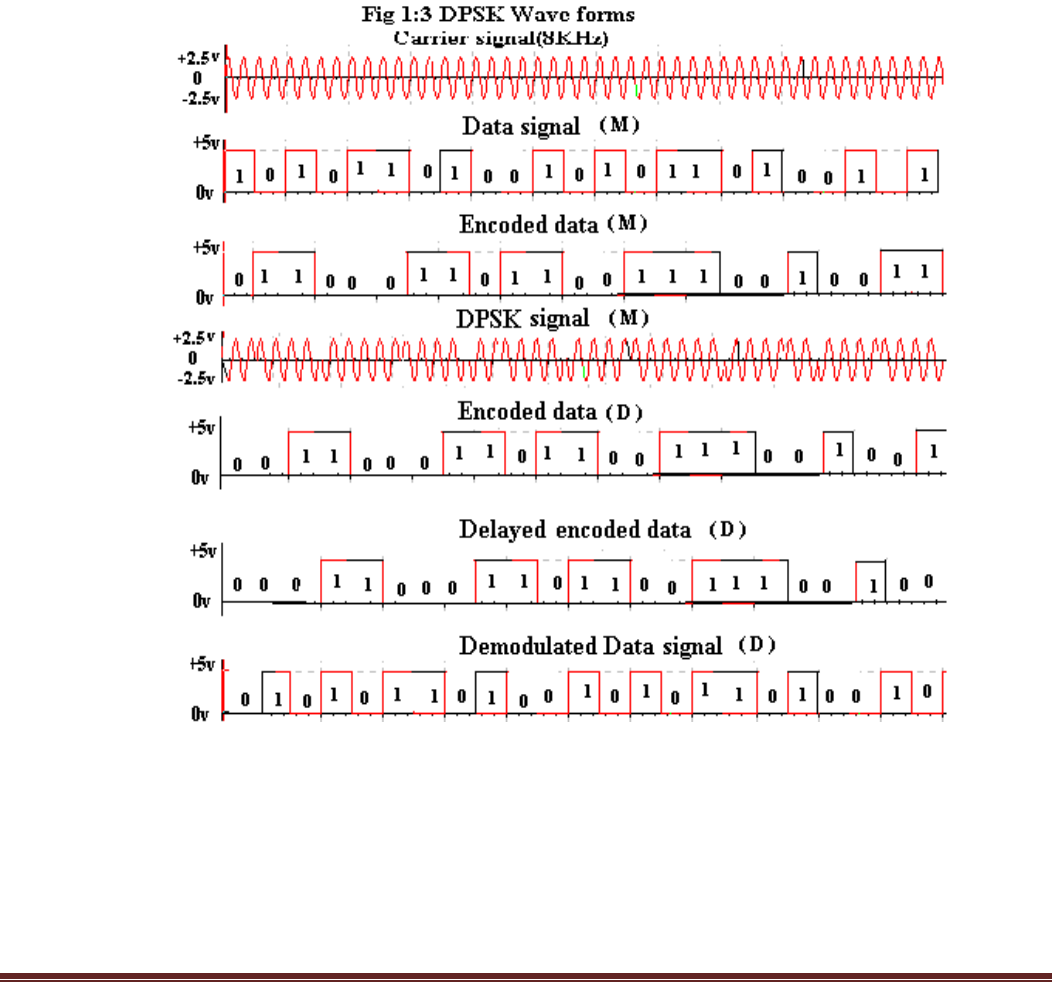
EXPECTED WAVEFORMS:
LAKSHMI NARAIN COLLEGE OF TECHNOLOGY, BHOPAL
Department of Electronics and Communication Engineering Page 44
OBSERVATIONS:
TYPE OF SIGNAL
AMPLITUD
E
FREQUENCY
BINARY DATA- 2KHz(Theoretical Rate )
BINARY DATA - 4 KHz (Theoretical Rate )
BINARY DATA - 8 KHz (Theoretical Rate )
ENCODED DATA- 2KHz(Theoretical
Rate ) WITH VALUE
ENCODED DATA - 4 KHz (Theoretical Rate
)WITH VALUE
ENCODED DATA -8 KHz (Theoretical Rate
)WITH VALUE
CARRIER SIGNAL
MODULATED SIGNAL
RECOVERED DECODED DATA
RECOVERED BINARY DATA
RESULT:
Thus the DPSK modulation and demodulation were performed and waveforms were plotted.
VIVA QUESTIONS:
1. Define DPSK?
2. Mention the advantages of DPSK?
3. Mention the disadvantages of DPSK?
4. Draw the waveforms of DPSK?
5. Compare ASK, PSK, FSK and DPSK?
6. What are the applications of DPSK?
LAKSHMI NARAIN COLLEGE OF TECHNOLOGY, BHOPAL
Department of Electronics and Communication Engineering Page 45
Date of Experiment:_______________
EXPERIMENT NO: 9
AIM:
To perform modulation and demodulation of QPSK and sketch the relevant waveforms.
APPRATUS:
1. QPSK Trainer Kit
2. Dual Trace oscilloscope
3. Digital Multimeter
4. C.R.O (30MHz)
5. Patch chords.
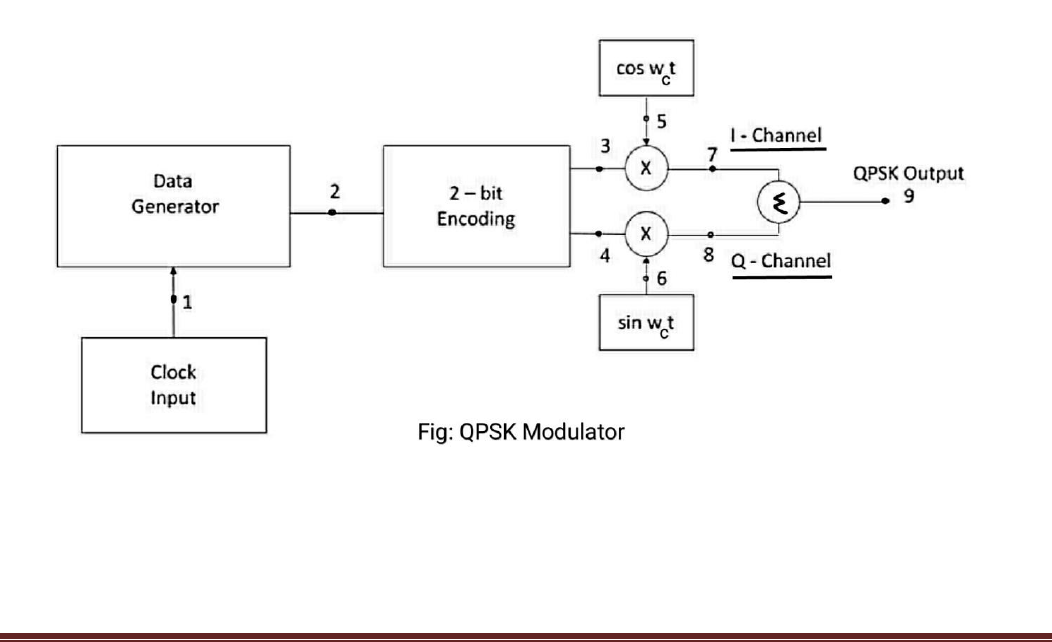
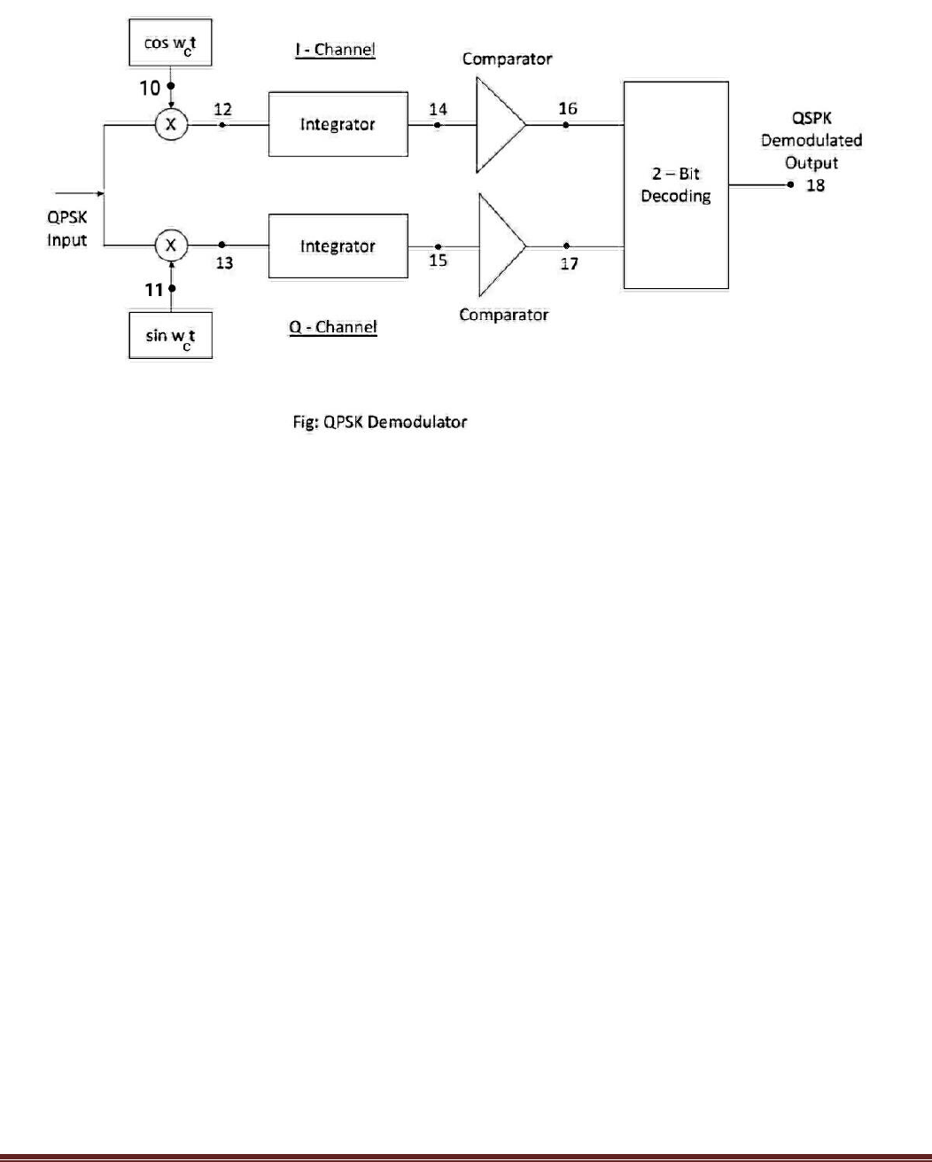
BLOCK DIAGRAM:
QPSK MODULATOR AND DEMODULATOR
LAKSHMI NARAIN COLLEGE OF TECHNOLOGY, BHOPAL
Department of Electronics and Communication Engineering Page 46
THEORY:
Quadrature Phase Shift Keying
Phase of the carrier takes on one of our equally spaced values such as π/4, 3π/4, 5π/4,7π/4.
Si(t) = √2E/ Tb cos{2 πƒct + (2i – 1) π/4} , 0≤ t ≤ Tb
0, ,elsewhere
Where i=1,2,3,4,and E=Tx signal energy per symbol
T
b
= symbol duration
Each of the possible value of phase corresponds to a pair of bits called dibits.
Thus the gray encoded set of dibits: 10, 00, 01,11
Si(t) =√2E/T
b
cos [(2i– 1)π/4] cos (2πfct) -√2E/T
b
sin [(2i–1) π/4)] Sin
(2πfct) , 0≤ t ≤Tb 0 , else where
There are two ortho nonormal basis functions
Ø1 (t) = √2/ Tb cos 2πƒct, 0≤ t ≤Tb
Ø2 (t)= √2/Tbsin2πƒct,0≤t≤Tb
The i/p binary sequence b(t) is represented in polar form with symbols 1 and 0 represented as
+√E/2 and -√E/2 .This binary wave is Demultiplexed into two separate binary waves consisting
of odd and even numbered input bits denoted by b1 (t) & b2 (t)
b1(t)andb2(t) are used to modulate a pair of quadrature carrier or orthogonal Basis function Ø1
(t) and Ø2(t).The result is two PSK waves’. These two binary PSK waves are added to produce
the desired QPSK signal .

LAKSHMI NARAIN COLLEGE OF TECHNOLOGY, BHOPAL
Department of Electronics and Communication Engineering Page 47
PROCEDURE:
1. Connect and switch ON the power supply.
2. QPSK is selected by default and LEDs of corresponding technique will glow.
3. Select the bit pattern using push button i.e.8 bit or 16 bit or 32 bit or 64 bit. Observe bit
pattern on TP-2.
4. Select data rate using push button i.e. 2 KHz or4 KHz or 8 KHz or 16KHz.
Modulation:
5. Observe the input bit pattern by varying bit pattern using respective push button.
6. Observe the data rate by varying data rate using respective push button.
7. Observe the Two-bit encoding i.e. I-Channel and Q-Channel.
8. Observe carrier signal i.e. cosine wave and sine wave .Frequency of carrier signal will change
with respect to data rate.
9. Observe I-Channel and Q-Channel modulated signal.
10. Observe QPSK modulated signal.
Demodulation:
11. Apply the QPSK modulated output to the demodulator input.
12. Observe the multiplied signal of QPSK and carrier signal, cosine and also observe the
multiplied signal of QPSK and carrier signal, sine.
13. Observe the integrated output at I-channel and Q-channel
LAKSHMI NARAIN COLLEGE OF TECHNOLOGY, BHOPAL
Department of Electronics and Communication Engineering Page 48
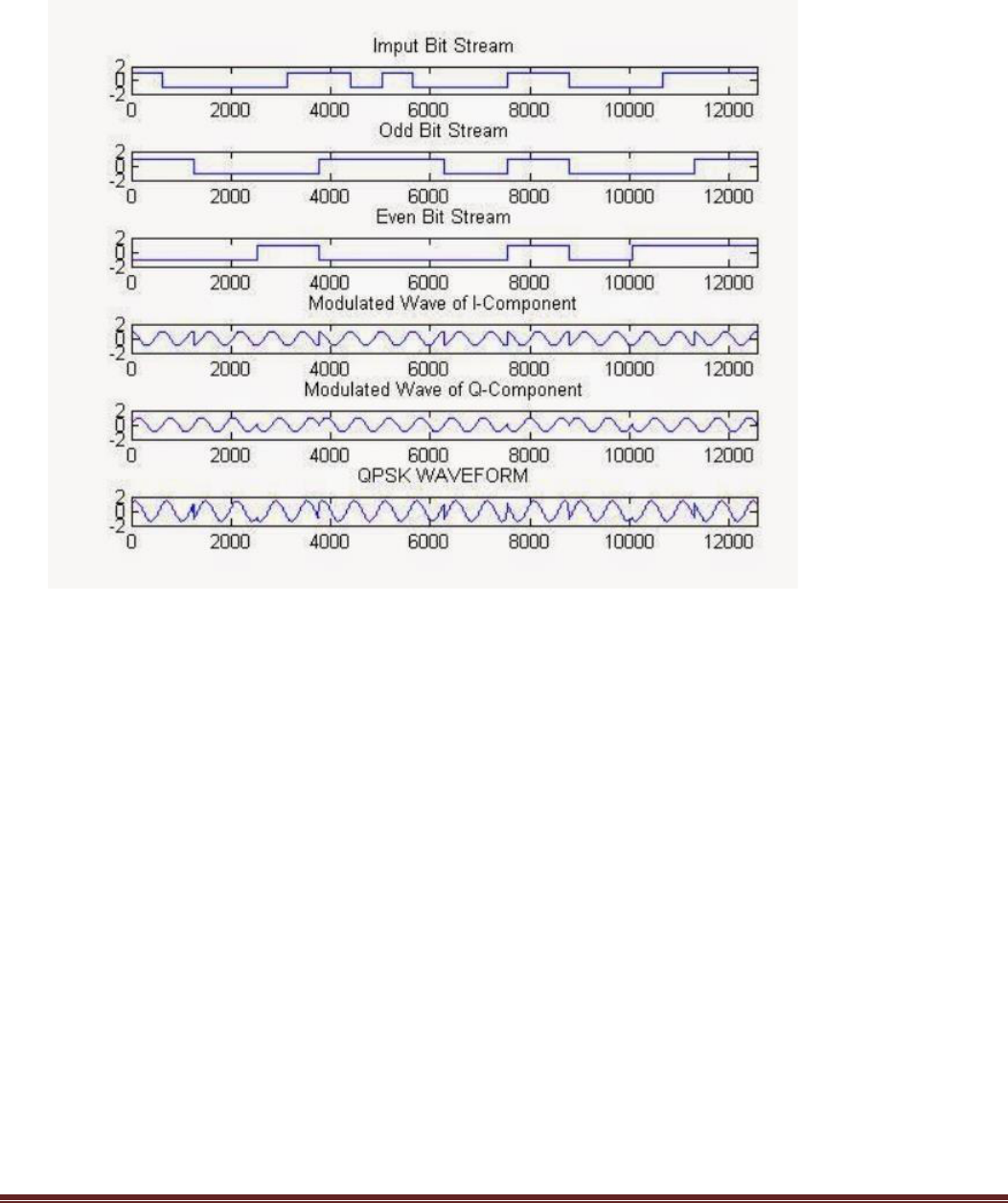
EXPECTEDWAVEFORMS:
RESULT:
QPSK modulation and demodulation waveforms are observed.
VIVA QUESTIONS:
1. Draw the constellation diagram of QPSK.
2. Give some applications of QPSK modulation scheme
3. Give the Bandwidth of QPSK signal
4. What is the relationship between 4 QAM and QPSK?
5. QPSK is an example of which M-ary technique.
LAKSHMI NARAIN COLLEGE OF TECHNOLOGY, BHOPAL
Department of Electronics and Communication Engineering Page 49
Date of Experiment:_______________
EXPERIMENT NO: 10
AIM:
To analyze a DPCM system and to interpret the modulated and demodulated waveforms for a
sampling frequency of 2KHz, 4KHz and 8 KHz.
APPRATUS:
1. DPCM Modulation and Demodulation Trainer Kit
2. Dual Trace oscilloscope
3. Digital Multi meter
4. C.R.O (30MHz)
5. Patch chords.
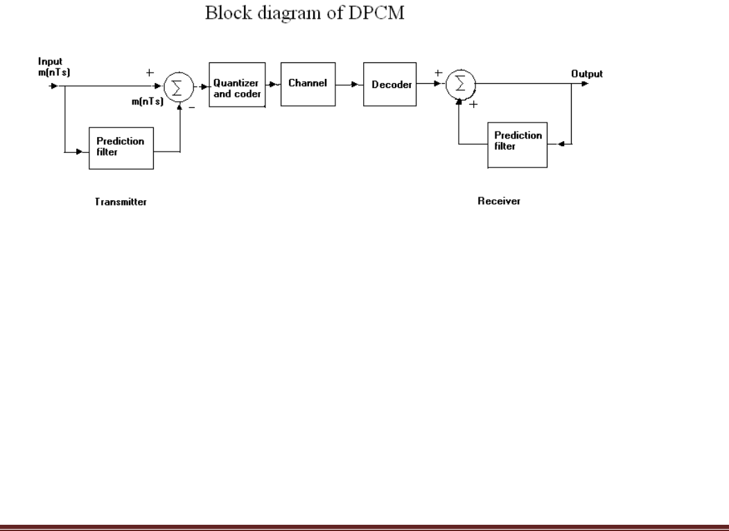
BLOCK DIAGRAM:
THEORY:
Differential PCM is quite similar to ordinary PCM. However, each word in this system indicates
the difference in amplitude, positive or negative, between this sample and the previous sample.
Thus the relative value of each sample is indicated rather than, the absolute value as in normal
PCM. This unique system consists of
DPCM Modulator
1. Regulated power supply
2. Audio Frequency signal generator
3. Prediction Filter

LAKSHMI NARAIN COLLEGE OF TECHNOLOGY, BHOPAL
Department of Electronics and Communication Engineering Page 50
4. Sample and Hold circuit
5. A/D Converter
6. Parallel to Serial Shift register
7. Clock generator/Timing circuit
8. DC source
II.
DPCM Demodulator
1. Regulated Power Supply
2. Serial to Parallel Shift registers.
3. D/A converter.
4. Clock generator
5. Timing circuit
6. Prediction filter
7. Passive low pass filter
PROCEDURE:
1. Study the theory of operation thoroughly.
2. Connect the trainer (Modulator) to the mains and switch ON the power supply.
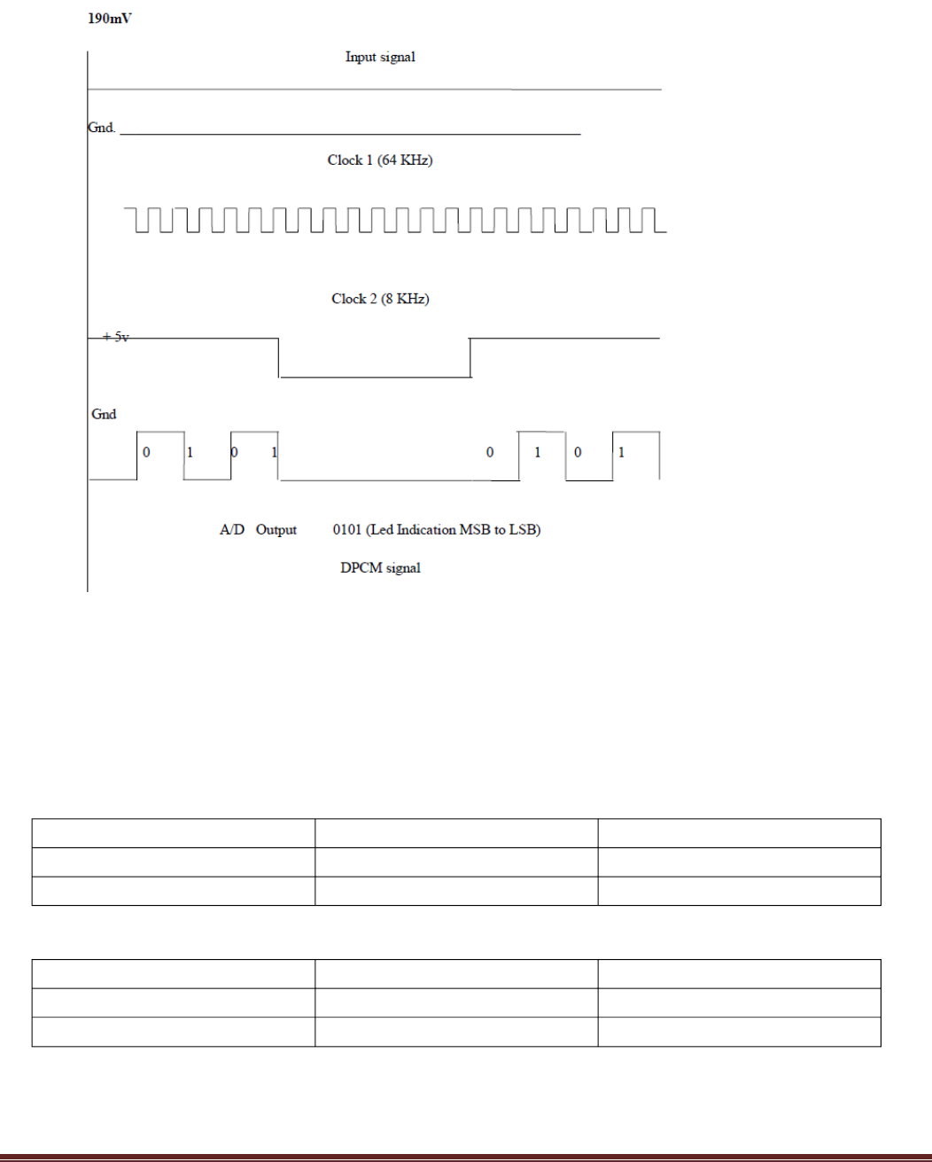
3. Observe the output of the AFgenerator using CRO, it should be Sine wave of 400Hz
frequency with 3V pp amplitude.
4. Verify the output of the DC source with multi-meter/scope ;output should vary 0to +290mV.
5. Observe the output of the Clock generator using CRO, hey should be 64 KHz and 8KHz
frequency of square with 5 Vpp amplitude.
6. Connect the trainer (De Modulator) to the mains and switch ON the power supply.
7. Observe the output of the Clock generator using CRO; it should be 64 KHz square wave with
amplitude of 5 pp.
DPCM Operation (with AC input):
Modulation:
1. Connect AC signal of 3VPP amplitude to positive terminal of the summer circuit.
Note :The output of the prediction filter is connected to the negative terminal of the summer
circuit and can observe the waveforms at the test points provided on the board.
2. The output of the summer is internally connected to the sample and hold circuit
3. Keep CRO in dual mode. Connect one channel to the AF signal and another channel to the
Sample and Hold output. Observe and sketch the sample and hold output
4. Connect the Sample and Hold output to the A/D converter and observe the DPCM output
using oscilloscope.

LAKSHMI NARAIN COLLEGE OF TECHNOLOGY, BHOPAL
Department of Electronics and Communication Engineering Page 51
5. Observe DPCM output by varying AF signal voltage.
Demodulation:
6. Connect DPCM signal to the demodulator input (S-P shift register) from the DPCM
modulator with the help of coaxial cable (supplied with trainer).
7. Connect clock signal (64KHz) from the transmitter to the receiver using coaxial cable.
8. Connect transmitter clock to the timing circuit.
9. Keep CRO in dual mode. Connect one channel to the sample and hold output and another
channel to the D/A converter output.
10. Observe ands ketch the D/A output
11. Connect D/A output to the LPF input and observe the output of the LPF.
12. Observe the waveform at the output of the summer circuit.
13. Disconnect clock from transmitter and connect to the local oscillator (i.e., clock generator
output from De Modulator) with remaining setup as it is. Observe D/A output and compare it
with the previous result. This signal is little bit distorted in shape. This is because lack of
synchronization between clock at transmitter and clock at receiver.
EXPECTEDWAVEFORMS:
The wave forms for the given AC input, corresponding binary data wave form, and for AC input
sample and hold waveforms are drawn then D/A converter o/p and then reconstructed AC
signal is also drawn.
LAKSHMI NARAIN COLLEGE OF TECHNOLOGY, BHOPAL
Department of Electronics and Communication Engineering Page 52
Amplitude
Time period
AC Input
Prediction Filter Output
OBSERVATIONS: DPCM with AC input
Sample and Hold Output
Clock -1 output
DPCM Output

LAKSHMI NARAIN COLLEGE OF TECHNOLOGY, BHOPAL
Department of Electronics and Communication Engineering Page 53
DPCM Input
D/A Converter Output
LPF Output
Demodulation Output
Prediction Filteroutput
Amplitude
Timeperiod
Demodulation:
RESULT:
Thus the Differential Pulse code modulation and demodulation were performed.
VIVAQUESTIONS:
1. For data compression says whether ADPCM or DPCM is better .Justify.
2. What is the need for compression ?Mention the types of compression.
3. List the communication standards which use DPCM.
4. Based upon the knowledge that you have gained after doing the experiment write
the Functions of sample and hold circuit.
5. Name the circuit used to achieve synchronization between transmitter and receiver.

LAKSHMINARAINCOLLEGEOFTECHNOLOGY,BHOPAL
Department of Electronics and Communication Engineering
Page 54
