
KIT – The Research University in the Helmholtz Association
www.kit.edu
Development of ASICs for particle physics and more..
Mridula Prathapan
ASIC and Detector Laboratory (ADL)
Institute of data Processing and Electronics (IPE)
2 25.02.2019
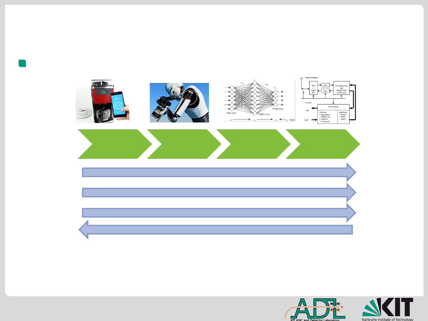
What are ASICs ?
ASIC stands for “Application Specific Integrated Circuits”
Microcontroller DSP FPGA ASIC
Signal Processing/Converter performance
Development Cost / Time
Power efficiency
Flexibility/Ease of design

3 25.02.2019
The LHC upgrade is by far the single largest ASIC demand for HEP
this decade
CMS Collaboration, ”CMS technical proposal: Upgrade of CMS detector through 2020,”
CERNLHCC-2011-06 (2013).
ATLAS Collaboration, ”Letter of Intent for the Phase-II Upgrade of the ATLAS
Experiment,” CERNLHCC-2012-022. (2013)
F. Anghinolfi, et. al., ”R&D Activities in Electronics for future HEP Experiments,”
submitted contribution to European Strategy Group, see CERN-ESG-005 (2013).
RD53 Collaboration, ”RD Collaboration Proposal: Development of pixel readout
integrated circuits for extreme rate and radiation,” CERN-LHCC-2013-008 (2013).
Demand for ASICs in HEP experiments
4 25.02.2019
Challenges in ASIC design for HEP
Technical challenges arise when
the performance needs to be significantly improved
when operating conditions lie well outside of industrial applications.
Modern ASIC design relies heavily on the accuracy simulation models
Power, Performance, Area trade off
High-bandwidth transmission
In-detector digitization, data reduction, processing
High dynamic range
Fast timing
Low cost and Reliability
Long development cycle with increase in complexity

5 25.02.2019
Outline of this talk
ASIC design at ADL
Chip design flow
ATLASpix chip design and testing
6 25.02.2019
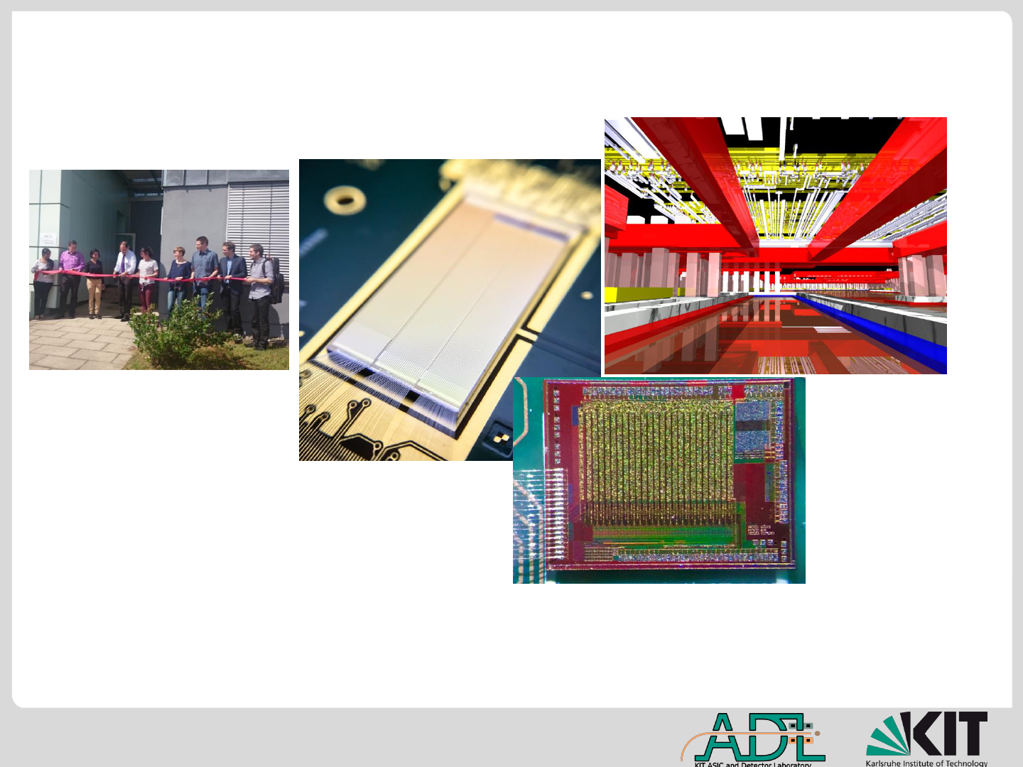
Inside view of DCD chip
ADL Lab inauguration in
2016 at KIT Campus Nord
ATLASpix1
Chip Photograph
Tape in : January 2017
ATLASpix2 TSI
Chip Micrograph
Tape in: September 2018
ADL lab at IPE
7 25.02.2019
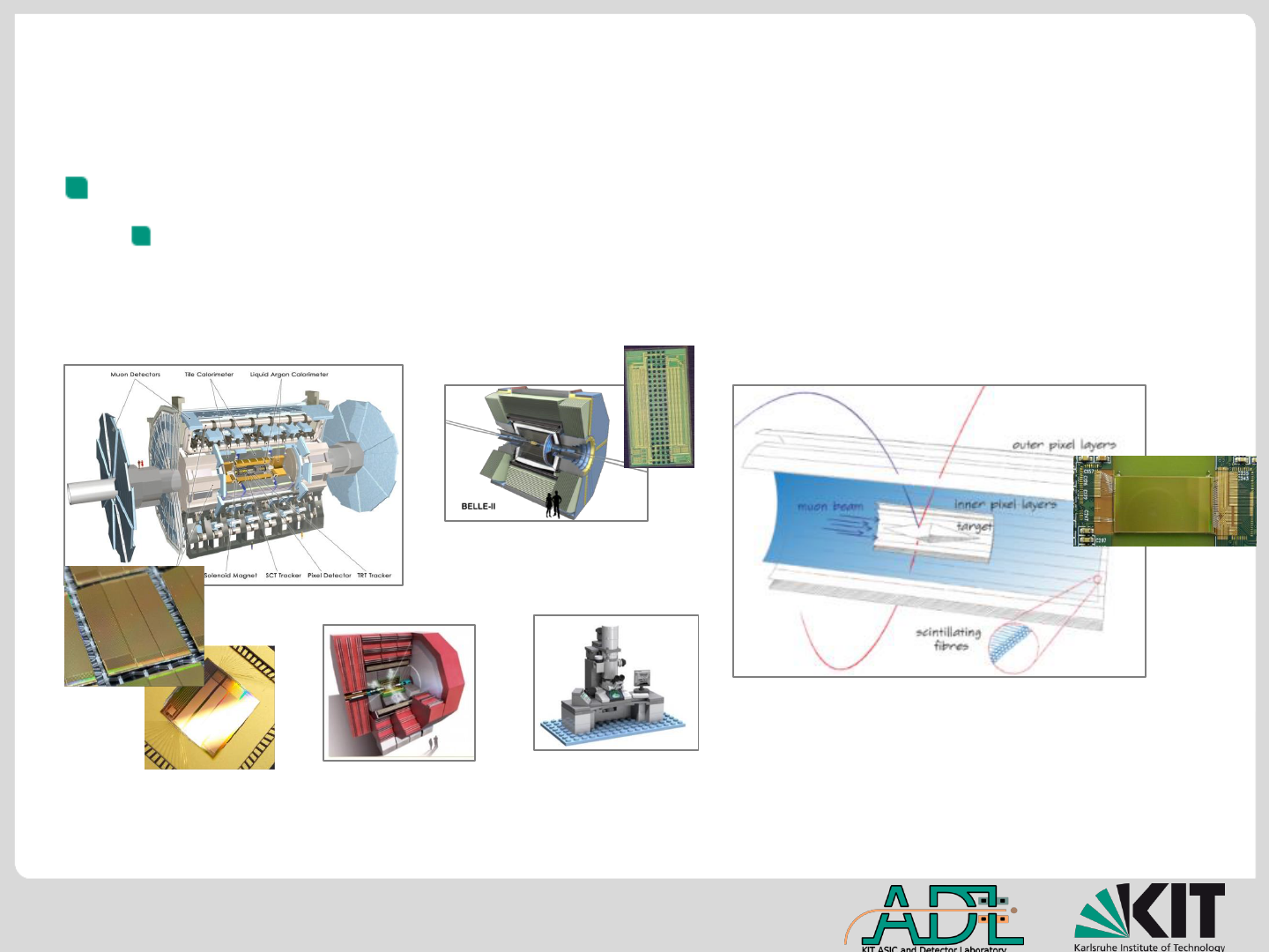
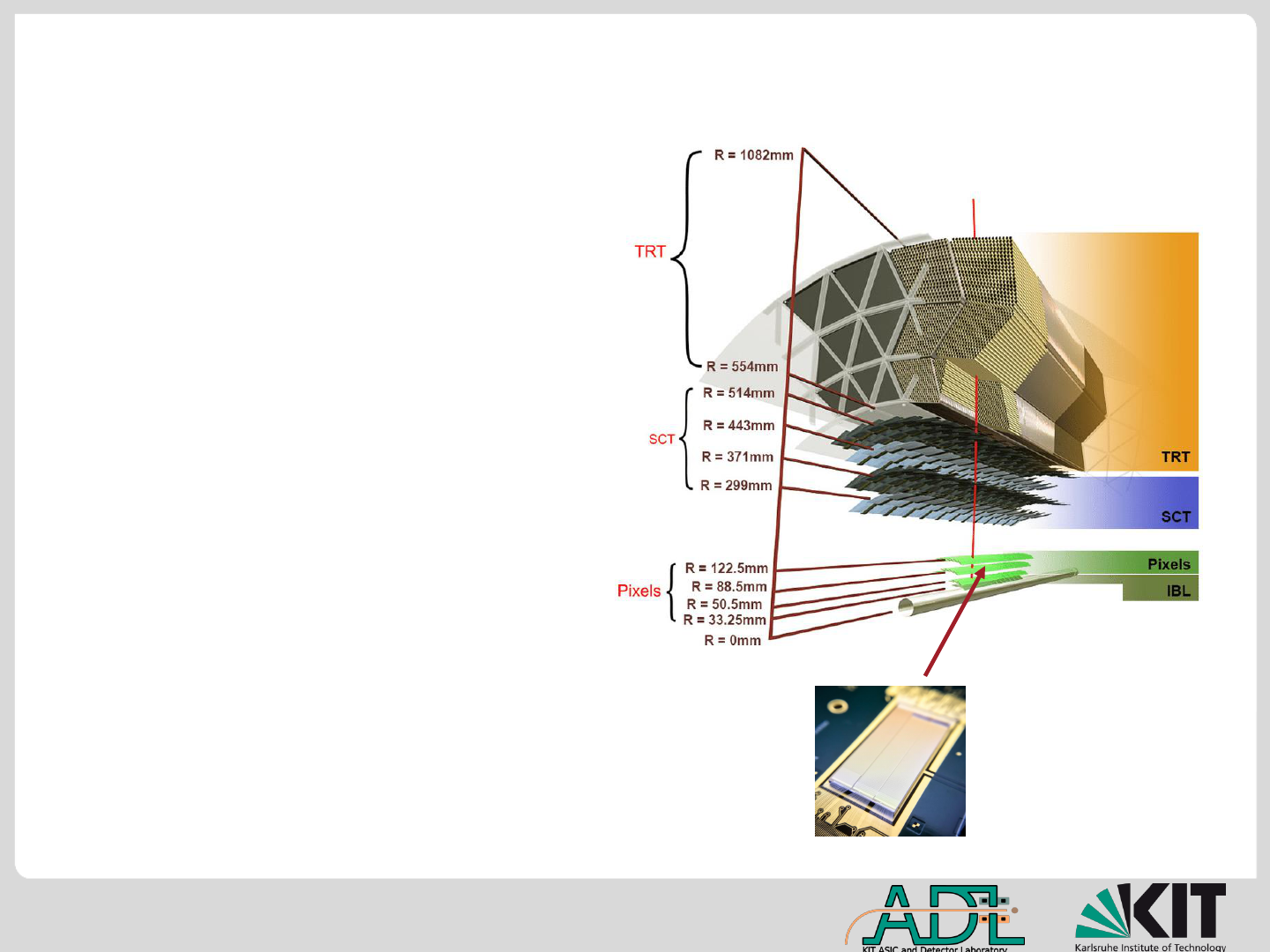
Applications
Semiconductor detectors for high energy physics
HVCMOS sensors are proposed cost-effective alternative to the
hybrid sensors for ATLAS Inner Tracker layer 4
ATLAS
Belle-II Mu3e
CLIC
Sensors for medical /
electron microscopy

8 25.02.2019
“Specify” your idea , Split it into blocks
Design the circuit
Make the chip testable
Ensure the design will work
Layout the chip
Double check the layout
Turn your design into silicon
Simple chip design flow
9 25.02.2019
Simple chip design flow
“Specify” your idea , Split it into blocks
Design the circuit
Make the chip testable
Ensure the design will work
Layout the chip
Double check the layout
Turn your design into silicon
Design Implementation
Logic
10 25.02.2019
Verification
Simple chip design flow
“Specify” your idea , Split it into blocks
Design the circuit
Make the chip testable
Ensure the design will work
Layout the chip
Double check the layout
Turn your design into silicon
Design Implementation
Logic
11 25.02.2019
Simple chip design flow
“Specify” your idea , Split it into blocks
Design the circuit
Make the chip testable
Ensure the design will work
Layout the chip
Double check the layout
Turn your design into silicon
Design Implementation
Logic
Verification
Design implementation
Physical design
Design for Manufacturing

12 25.02.2019
Step 1. “Specify” your idea
Today’s complex chip designs can have
a million lines of behavioral code.
Come up with a model of the chip
behaviour in a Hardware description
Language such as VHDL , Verilog,
System Verilog
Analog blocks such as pixels, amplifier,
comparator, DAC, PLL be modelled in
Verilog A or Verilog AMS
13 25.02.2019
Aim: Design an monolithic active pixel sensor chip in a
commercial CMOS process for ATLAS ITk pixel layer 4
2024/25: Phase 2 ATLAS will
completely replace its trackers
~ 160 m
2
silicon strips
~10 m
2
silicon pixel
Monolithic sensors saves bump bonding
for ~45% of outer barrel system
Substantial cost reduction and reduced
module assembly time
Advantages over hybrid sensors:

14 25.02.2019
Arrive at the design specifications
Feature
Specifications
Matrix size (row
, col)
372
x 132
Pixel size (x , y) µm
2
150 x 50
Readout scheme
Column drain readout
with trigger
SEU
SEU tolerant global
memory
Data encoding
Aurora 64b/66b
Output data rate
1.28
Gbps
CMD decoder
On
-chip CMD decoder
Serial powering
On
-chip
HL/LHC
Outer Pixel
NIEL[n
eq
/c
m
2
]
10
15
TID 80 Mrad
Hit rate
[MHz/cm
2
]
100-200
BC 25ns
SEU
affecting
pixel
100 / hour /
chip
Detection
efficiency
> 99%
Required on-chip design features
Harsh environment of
HL-LHC
15 25.02.2019
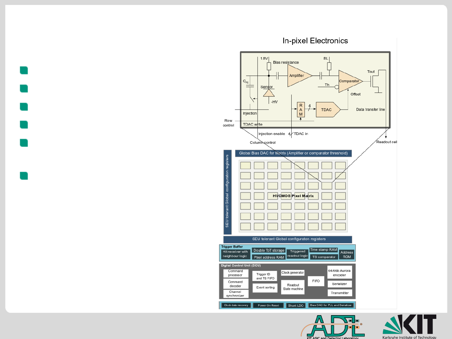
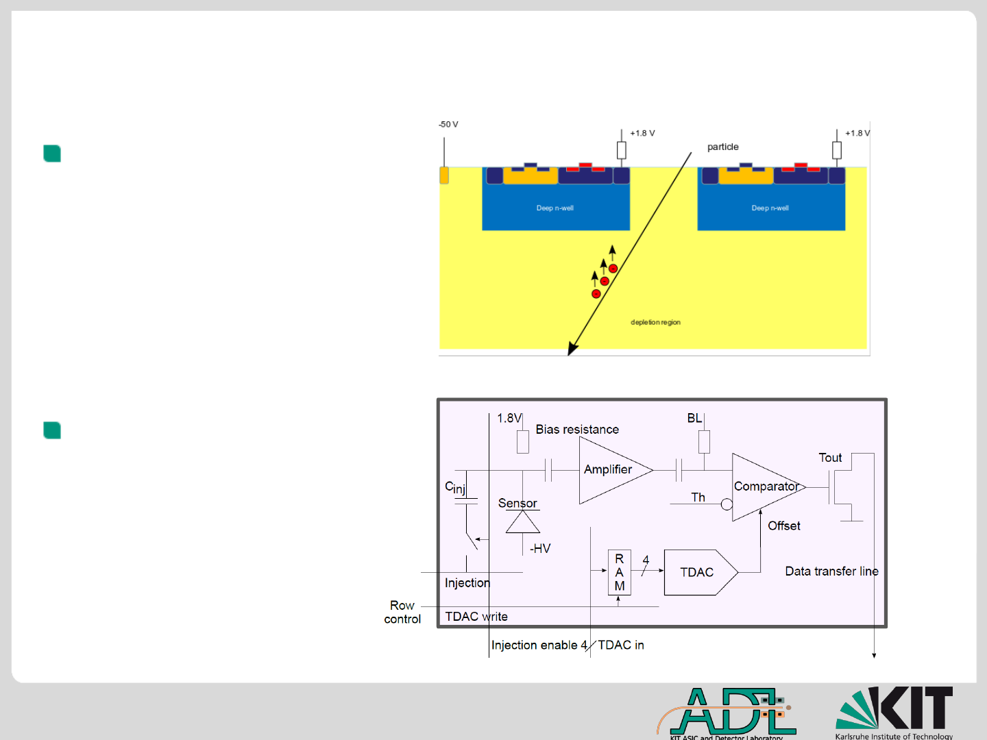
Split the specification into design blocks
Sensor
Pixel electronics
Readout electronics
Readout Control Unit
Design for configurability/
testability
Bias blocks, clock recovery,
POR etc (Analog Chip
Bottom (ACB))
16 25.02.2019
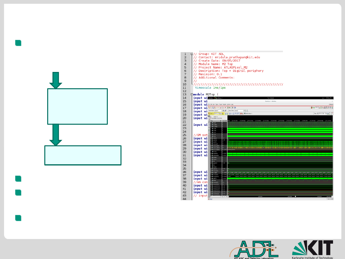
Behavioral model of the system eg: ATLASpix1_M2 chip
models the dynamic behavior of
the chip as it works
used for design verification
receiver block can be re-used in
firmware
saves the number of iteration cycles
Behavioral simulation of ATLASpix1 M2 chip
ATLASpix
Verilog Model
Binary hit pattern/
Command
Readout data
Receiver/Decoder

17 25.02.2019
Step 2, 3 & 4 : Design, simulation, verification
Example : ATLASpix design
18 25.02.2019
Design the circuit (Analog)
Sensor design
Pixel electronics
19 25.02.2019
The HVCMOS sensors allow construction of radiation hard particle
pixel detectors in standard CMOS technologies
Sensor operation
+1.8 V
0 V
+1.8 V
P substrate
Deep n-wellDeep n-well
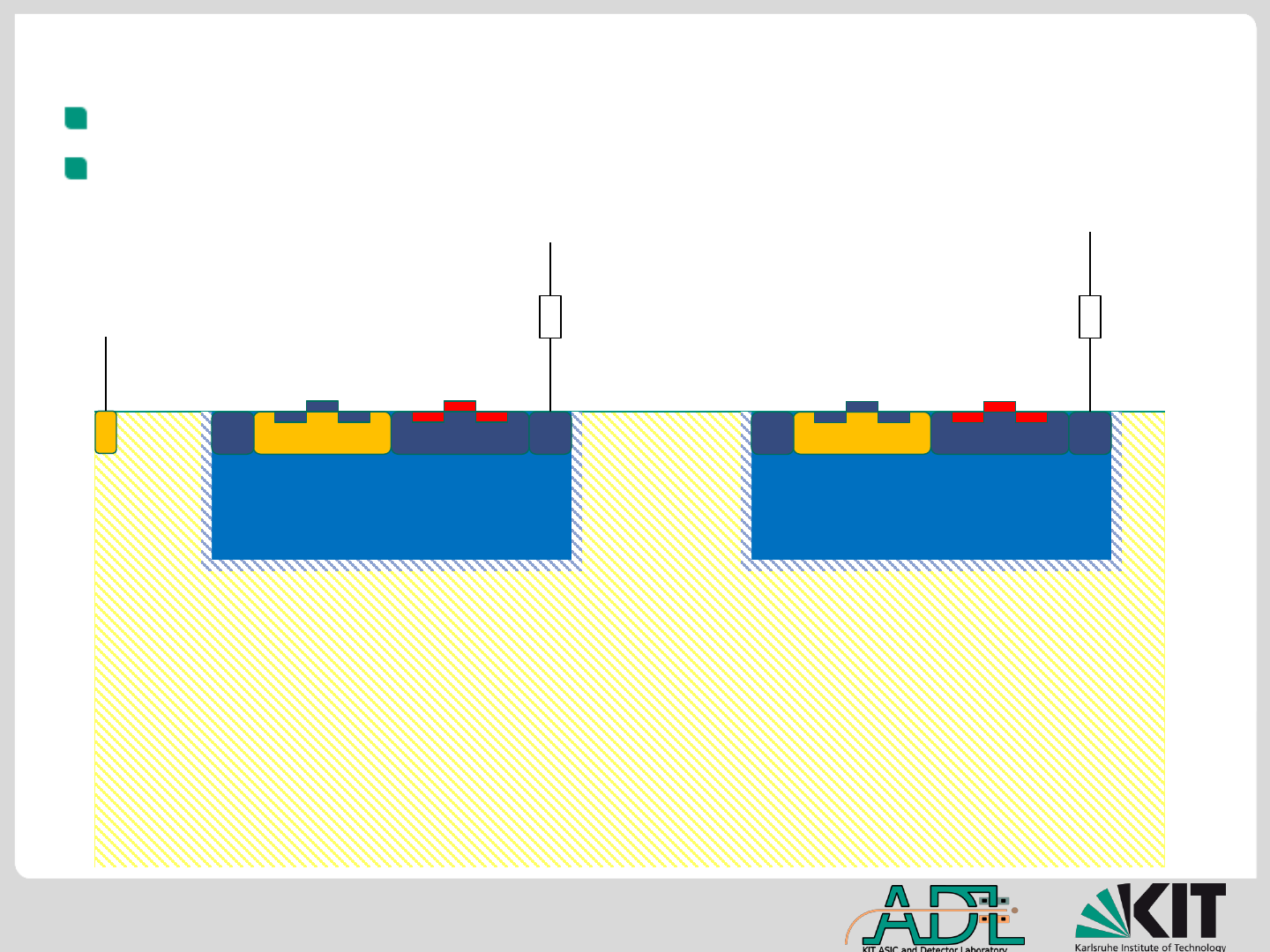
20 25.02.2019
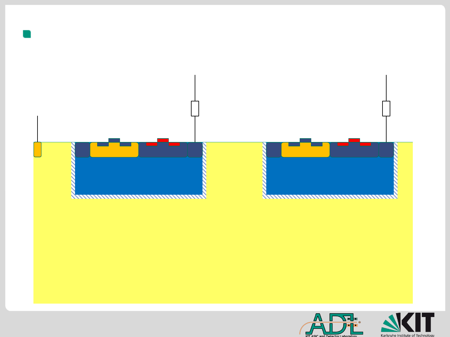
High resistivity substrates have been used (80Ωcm,200Ωcm,1kΩcm)
Induce space charge region by applying high voltage
+1.8 V
-50 V
+1.8 V
Deep n-well
Deep n-well
depletion region
21 25.02.2019
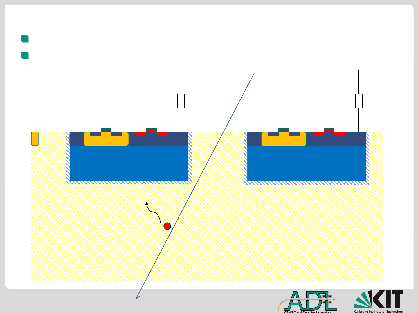
Faster charge collection by drift
Electronics are placed inside the charge collection well
+1.8 V
-50 V
+1.8 V
Deep n-well
Deep n-well
depletion region
-

22 25.02.2019
Advantages:
High radiation tolerance (fast charge collection, short drift path,
vertical depletion, no low field regions)
Biasing from front side (no need for backside contact)
Large depletion layer can be induced
Possibility to thin sensors to ~50µm
Disadvantages:
Detector capacitance (due to DNW-PW junction and DNW-P substrate)
23 25.02.2019
ATLASpix1 – Large area prototype
2.3 cm
1 cm
AMS ah18 Engineering
run
January 2017
Substrate resistivity
range
50Ωcm – 1kΩcm
Three design variants
based on
Readout scheme
The in-pixel
comparator design
Pixel has only CSA
and comparator
RO cells at the chip
periphery
Advantages:
No TS propagated
inside matrix-
smaller digital
power consumption
No digital crosstalk
Disadvantage:
Larger periphery
24 25.02.2019
Design the circuit (Digital (Full custom))
25 25.02.2019
26 25.02.2019
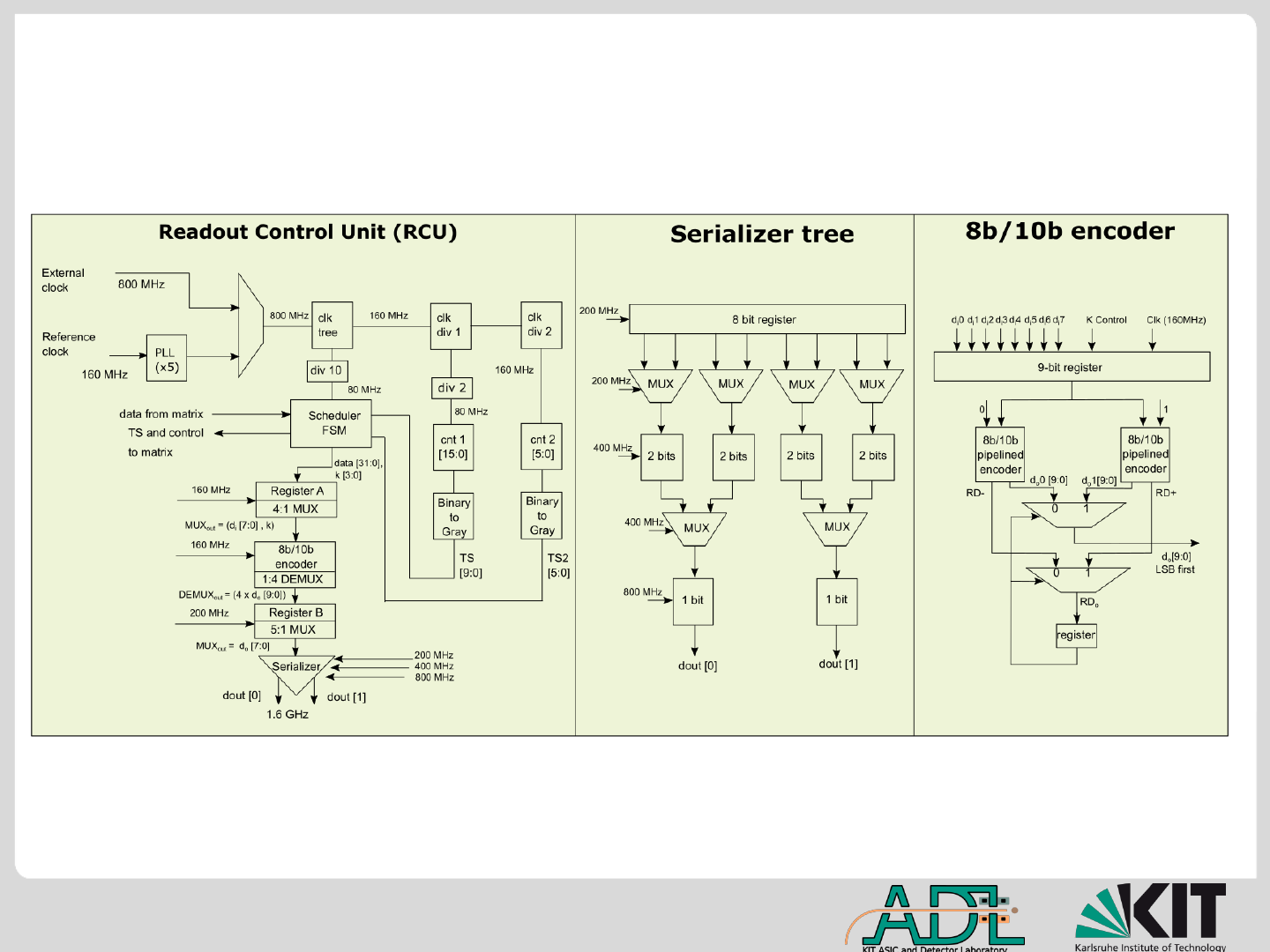
Design the circuit (Digital(semi custom))
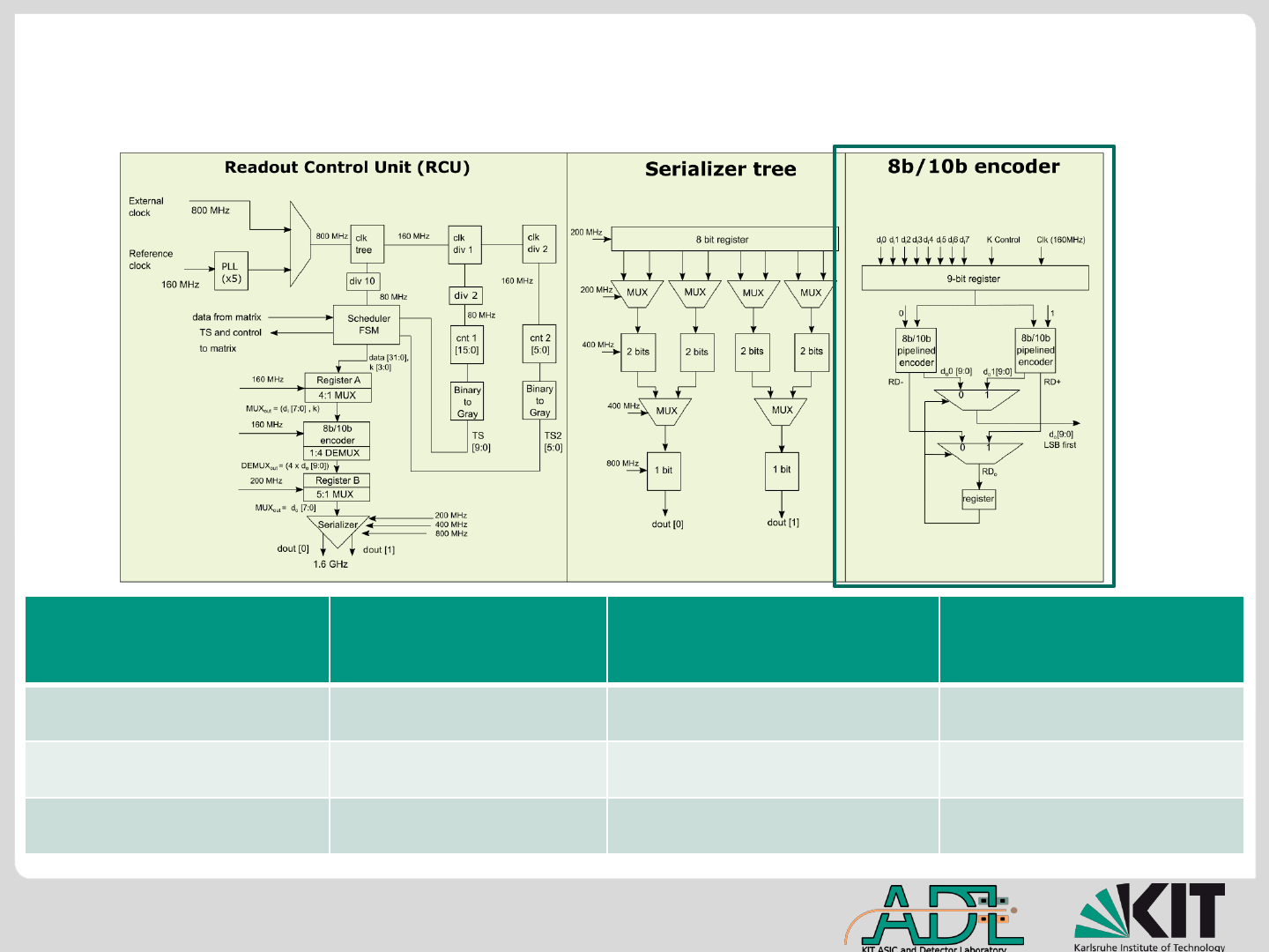
27 25.02.2019
Design the circuit (Digital(semi custom))
Cadence
soft IP
Open source (based
on IBM IP)
A pipelined 8b/10b
encoder
( KIT)
Power
5.5
mW
1.5
mW
5
mW
Performance
4.8
Gbps
5.8
Gbps
6.2
Gbps
Area
0.045 mm
2
0.02
mm
2
0.045 mm
2
28 25.02.2019
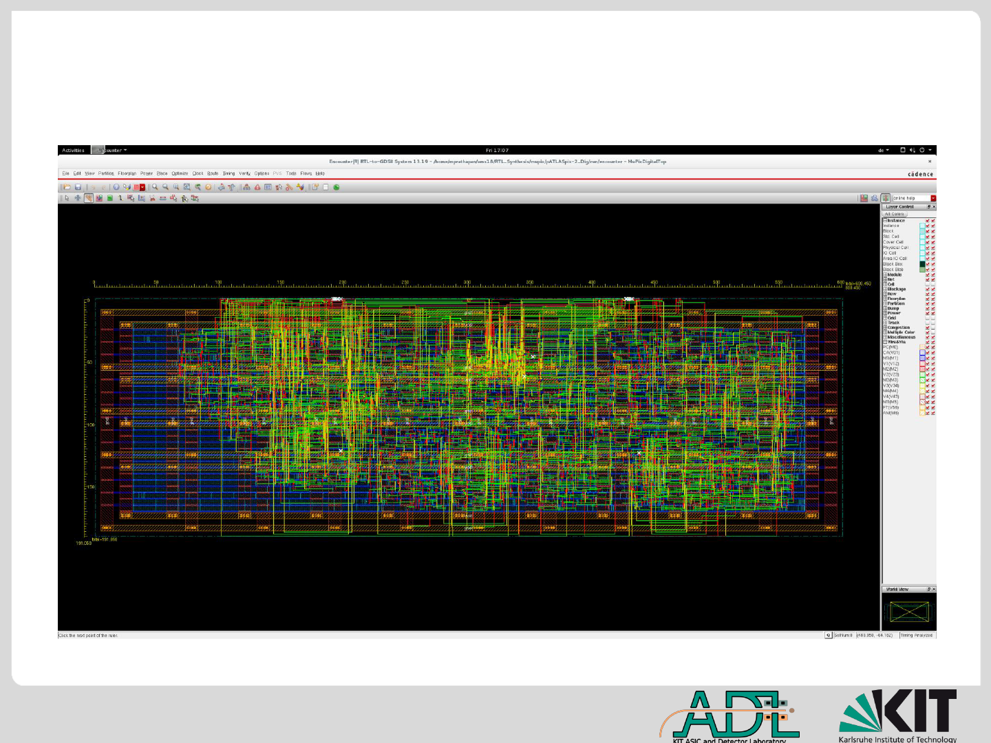
Step 5 : Design for manufacturing /
physical design
29 25.02.2019
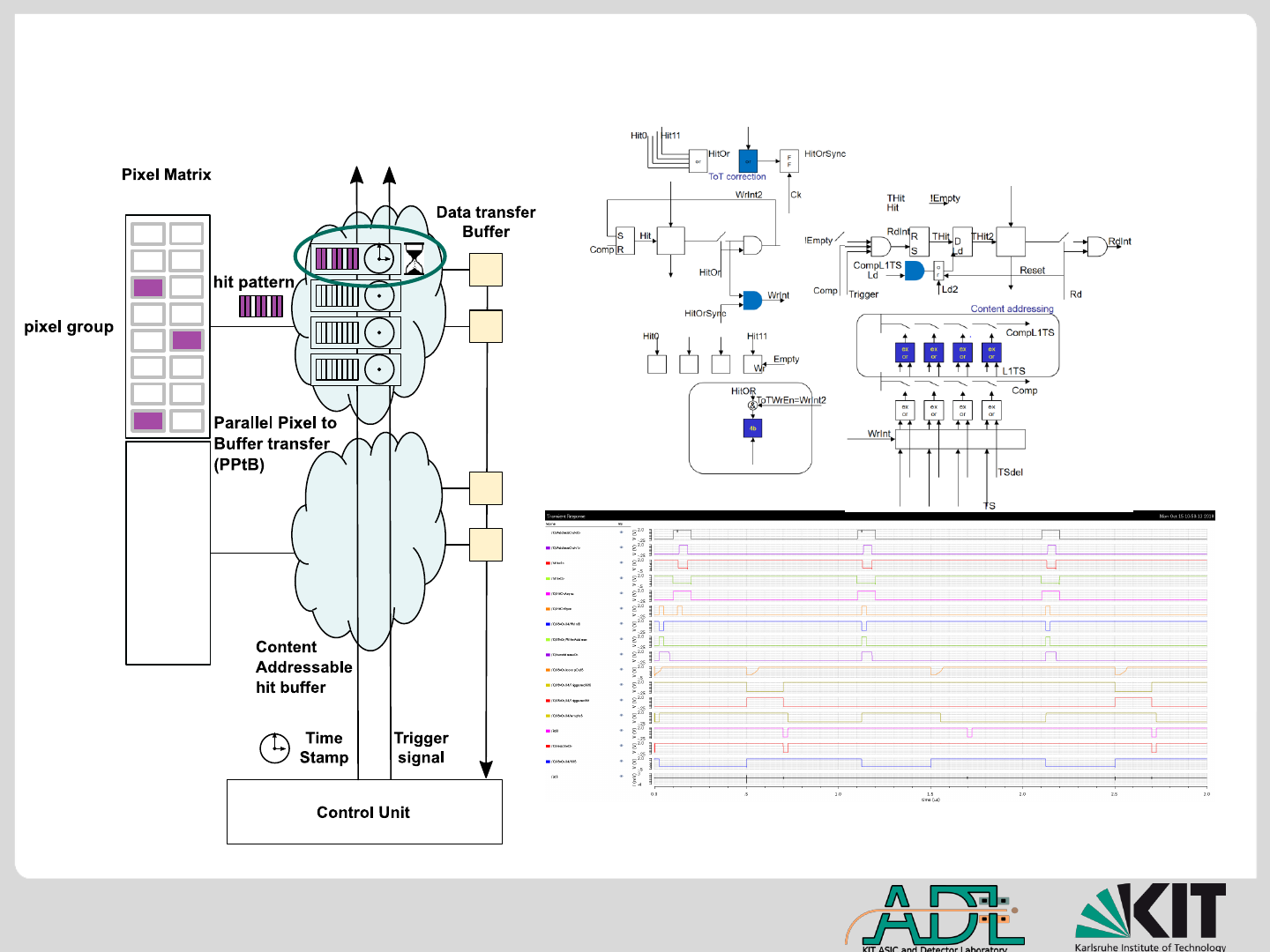
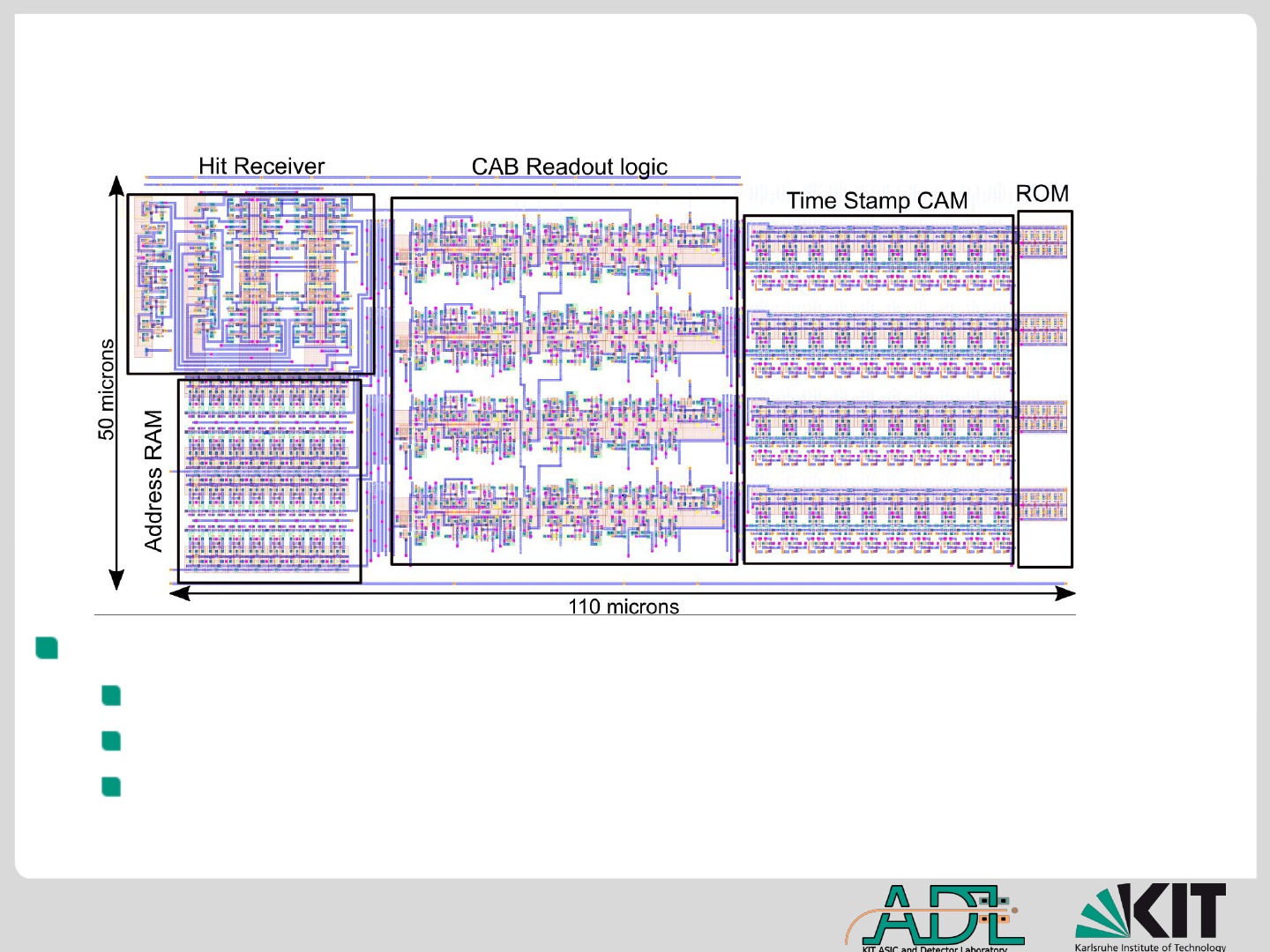
Trigger buffer (full custom) eg: ATLASpix1 M2
Stores the following hit data until “on-chip programmable latency”
Time stamp – 10bits
Address – 8 bits
Group address - 6 bits
30 25.02.2019
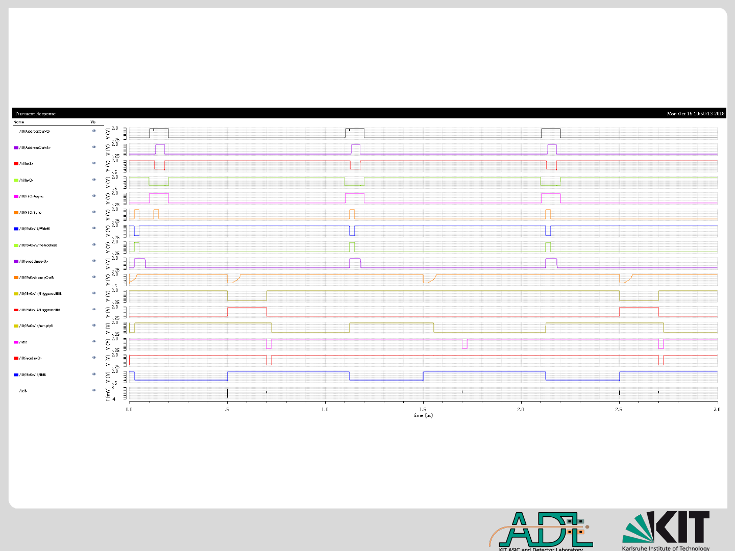
Readout control unit (semi custom) eg: ATLASpix2
31 25.02.2019
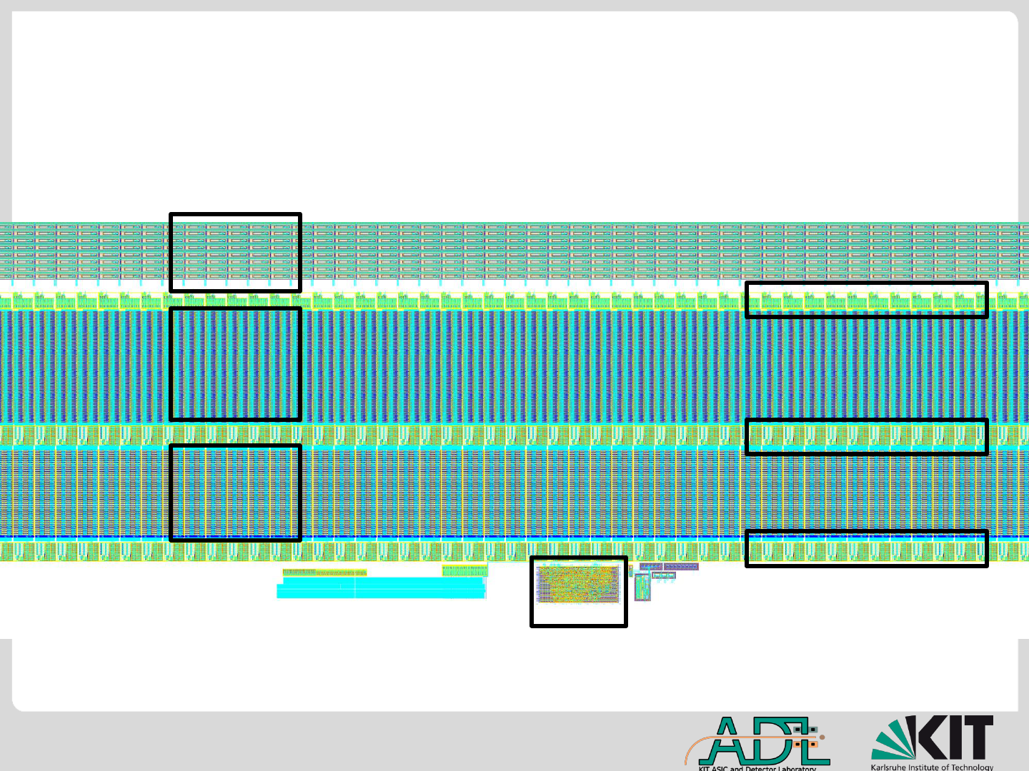
Chip integration of ATLASpix3
Pixels
Hit Buffers
Trigger
Buffers
EoC1
EoC2
Config. reg
RCU
32 25.02.2019
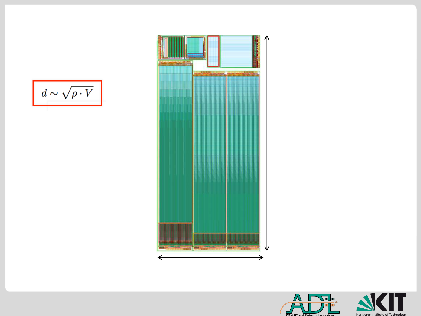
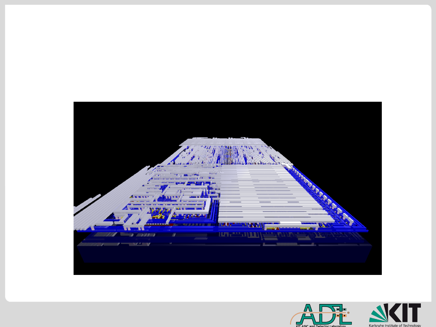
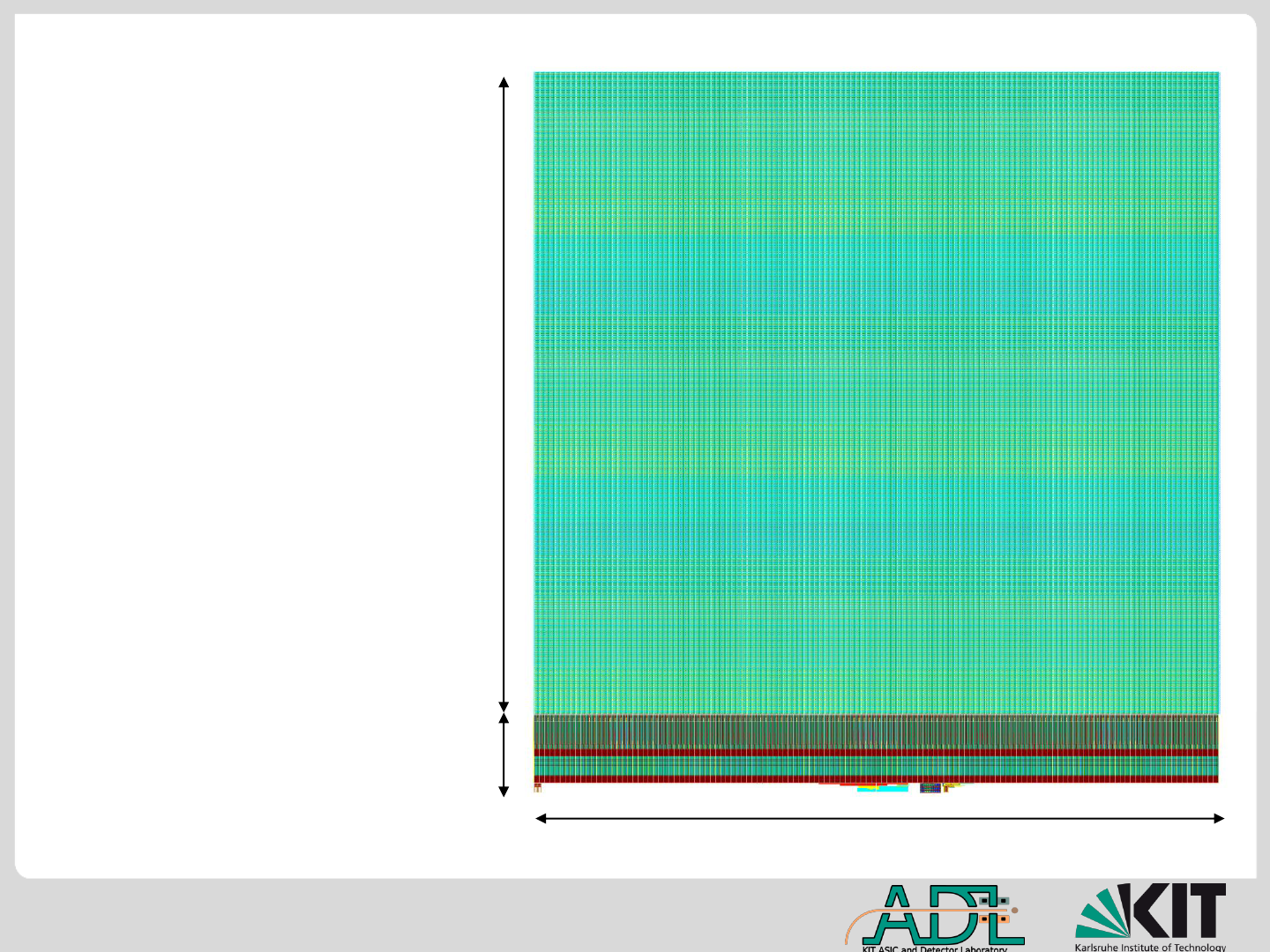
Full chip layout
ATLASpix 3
0.2 cm
1.8 cm
2 cm
Pixel Matrix
Periphery
Dimensions : 2 cm x 2 cm
Chip periphery occupying
10% of the total area
To be used for HVCMOS
quad module construction
Planned submission:
March 1
st
2019

33 25.02.2019
Post silicon testing of ATLASpix1_M2
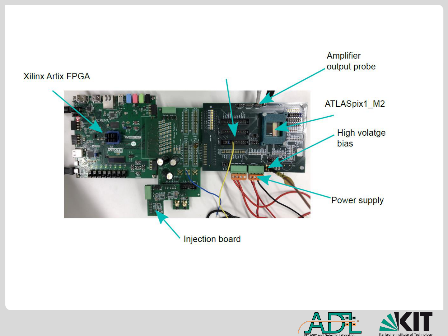
34 25.02.2019
Test system
(developed by Felix Ehrler, see
talk on Wednesday)
35 25.02.2019
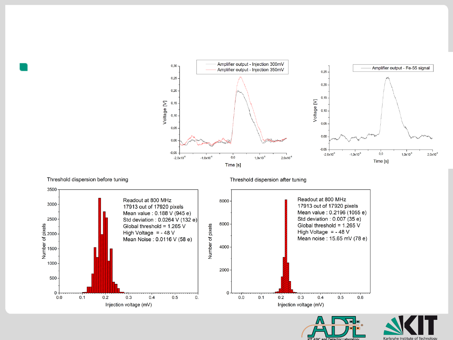
ATLASpix1_M2 measurements
Threshold tuning
36 25.02.2019
ATLASpix1_M2 measurements
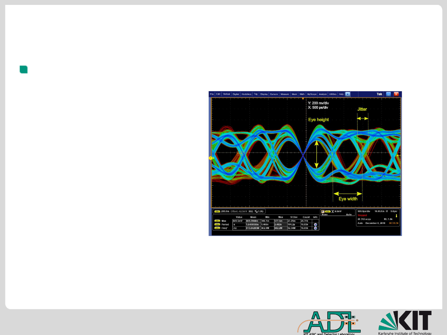
Eye diagram at 1.28 Gbps
eye height ~ 504 mV,
eye width ~ 580 ps
jitter ~ 100 ps

37 25.02.2019
ATLASpix design summary
ATLASpix (1,2,3) series in AMS/TSI 180nm CMOS process
Full chip Verilog model for verification
novel design concepts such as the Parallel
Design of hit data memory (SRAM array)
Trigger buffer design that holds the hit data until readout
Analysing memory design in order to efficiently use bandwidth, low
power and area
Design of Readout Control Unit to schedule the entire readout operation
Novel MUX based serializer architecture and data encoder designs
Command decoder that receives command words and clock recovery
from Clk/CMD 160MHz

38 25.02.2019
ATLASpix1_M2 Testing Summary
SNR of about 64 was measured
The power consumption of ATLASPix_M2 is about 300mW/cm
2
The 2/3 of the power is from comparators, buffers, digital block. 1/3 from
pixel amplifiers
The serial data link works at the required data rate of 1.28 Gbps
The time walk for signals from 1500e (20% MIP) to 9000e (130% MIP)
is typically 35ns.
Test beam and irradiation studies on ATLASpix1 prototypes are being
conducted within the collaboration of six different institutions
ATLASpix1 series is fully functional

39 25.02.2019
Thank you for your attention

40 25.02.2019
Back up
41 25.02.2019
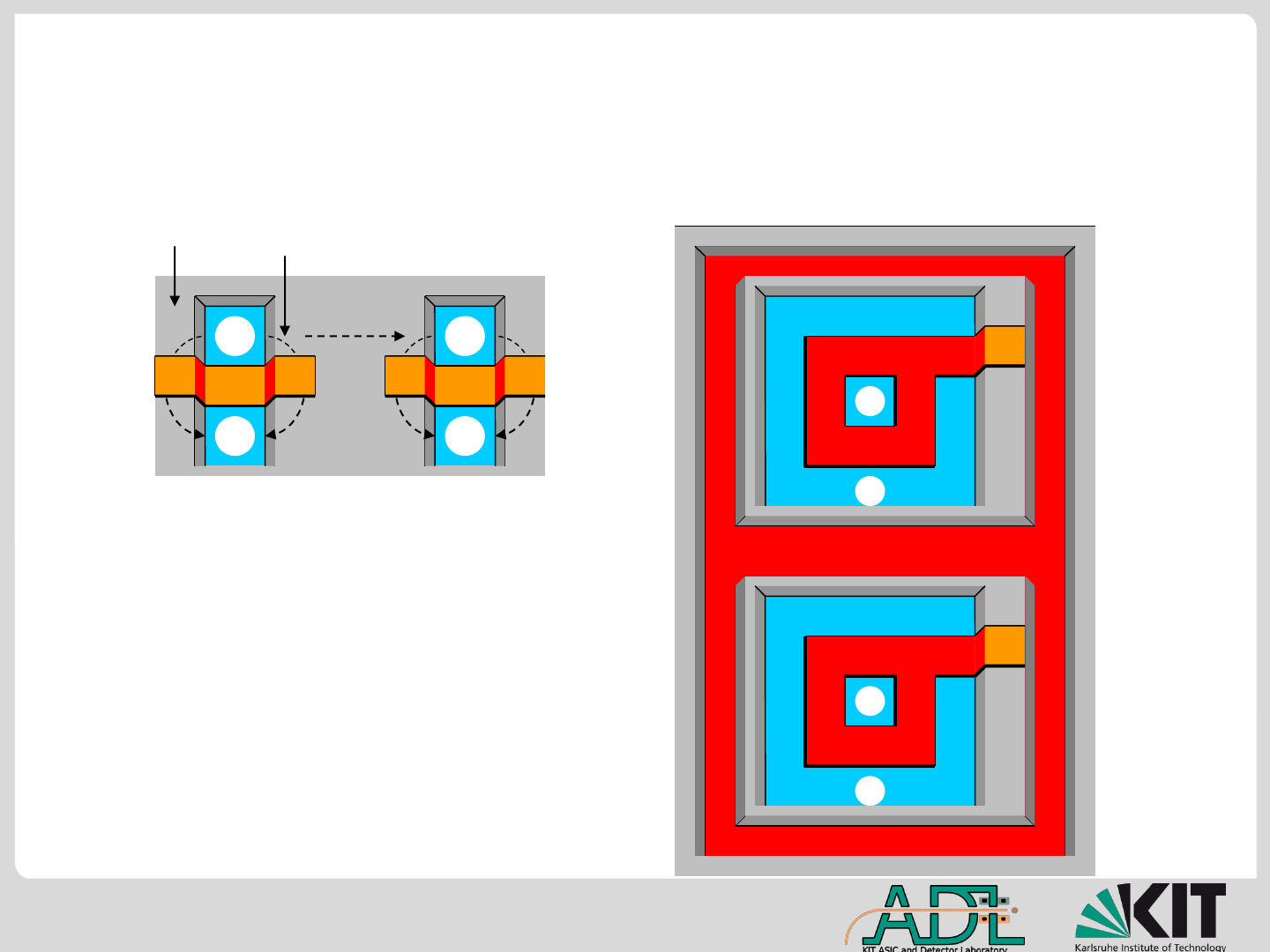
41
D
S
Field oxide
Leakage current
Standard NMOS
Annular gate NMOS
G
Standard- and annular NMOS transistors
D
S
G
D
S
G
D
S
G
Guard ring
P+
N+
42 25.02.2019
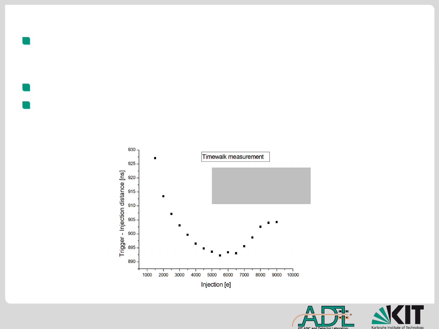
We can measure the trigger window characteristics by varying the
trigger vs injection time distance. It the distance is too small the hits
are not triggered and deleted. An S-curve is the result
In this way the time resolution and time walk can be measured
The time walk for signals from 1500e (20% MIP) to 9000e (130% MIP)
is typically 35ns.
Trigger vs injection
distance where 50% of
the hits are detected
43 25.02.2019
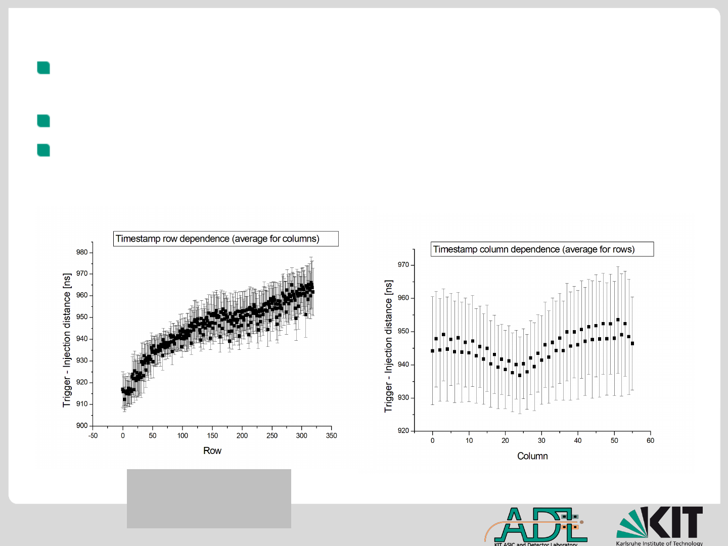
There is the skew of the hit-timing (time walk) that depends on the row
of the pixel in matrix.
The time skew is about 45ns from row 0 to maximum row 319
The reason for skew is different length and different capacitive load of
the long lines. It will be fixed in next large submission. All lines will
have the same length. Digital correction is also possible
Column dependence of timing is smaller – about 10ns. It is probably
caused by voltage drops
Trigger vs injection
distance where 50% of
the hits are detected
44 25.02.2019
…
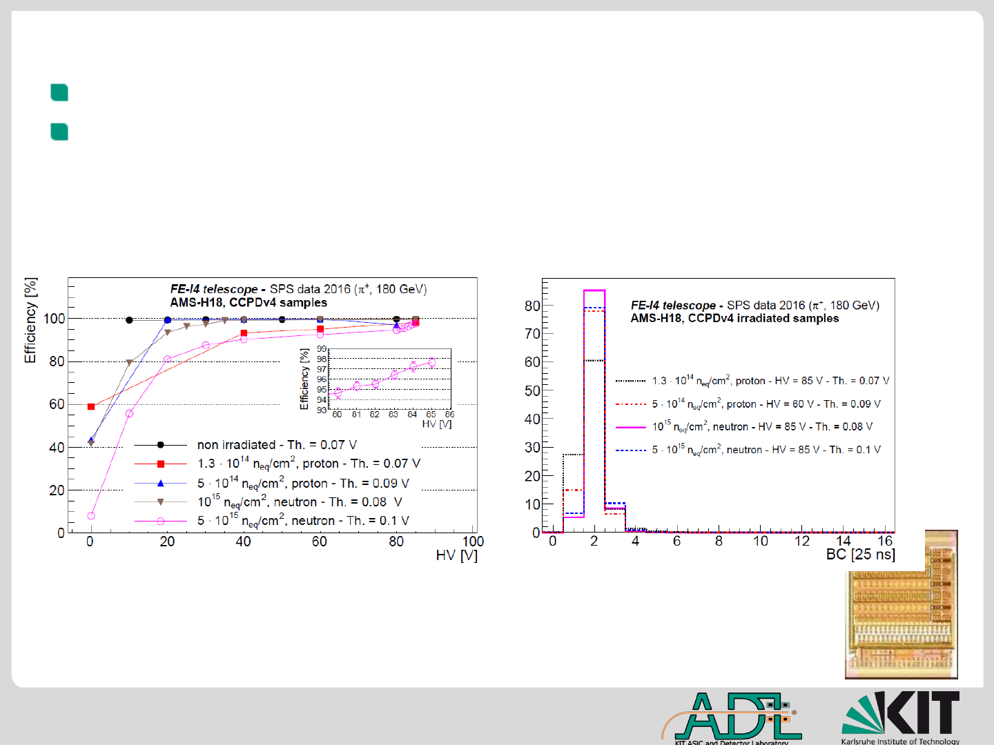
Achievements:
Time resolution ~ 25ns, radiation hardness of 100MRad and 5x10
15
n
eq
/cm
2
. Fast readout on sensor chip with high bandwidth amplifiers.
Possibility to thin sensors to ~50µm.
M. Benoit et al.,
“Testbeam results of irradiated AMS H18 HV-CMOS pixel sensor prototypes”
arXiv:1611.02669 [physics.ins-det]
Low resistivity
Absolute efficiency measured
>99%
Whole matrix used (full readout)
2 bins 95%
